downloadGroupGroupnoun_press release_995423_000000 copyGroupnoun_Feed_96767_000000Group 19noun_pictures_1817522_000000Member company iconResource item iconStore item iconGroup 19Group 19noun_Photo_2085192_000000 Copynoun_presentation_2096081_000000Group 19Group Copy 7noun_webinar_692730_000000Path
Skip to main content
Default Banner Image

Technology and Trends

Advanced packaging is no longer operating behind the scenes. The technology of advanced packaging is helping to sustain the speed of the semiconductor industry’s improvement in power and performance, even as the Moore’s Law roadmap for wafer-level scaling comes under strain.At the Advanced Packaging Conference during SEMICON Europa 2025 in Munich, global experts examined the growth trajectory of this critical sector and Europe’s potential to lead in next-generation packaging solutions.Market Momentum Fueled by AI and HPCRomain Fraux, Chief Research Officer at Yole Group, forecasted that global revenues for advanced packaging will grow from $46.1 billion in 2024 to $79.4 billion by 2030. “Everything is linked to AI and high-performance computing (HPC),” said Fraux, while also emphasizing the growing relevance of automotive applications in driving demand.Romain Fraux, Chief Research Officer, Yole GroupThis demand is accelerating innovation across the supply chain. One emerging area is panel-level packaging, which breaks away from traditional round wafers. As Andreas Wocko, Sales Manager at Lam Research, observed, “Since the 1970s, the semiconductor industry has built on wafers. Now we are not just scaling, we are reshaping, building in a square format for the first time” – an innovation which substantially increases area efficiency and reduces device cost. Andreas Wocko, Sales Manager Europe, Lam ResearchTechnology Transformation from Lab to FabEurope is already investing in the foundational technologies that will power tomorrow’s packaging systems. Rolf Aschenbrenner, Deputy Director of Fraunhofer IZM, the home of the European Union’s APECS advanced packaging pilot line, discussed ongoing research into functional interposers, routing density, and organic interposers. “Our goal is to show how a new design philosophy incorporating chiplets can be brought to the industrial systems level,” said Aschenbrenner.Rolf Aschenbrenner, Director Deputy, Fraunhofer IZMThese breakthroughs are essential, as pitch sizes shrink and new materials emerge. Dr. Jessica Stubbe, Global Application Manager at MKS Atotech, described how interconnect densities have doubled in the past two years, with the industry moving to pitch sizes of less than 10µm. Stubbe said this new technology “will be enabled by a move from traditional solder-based interconnects to copper-to-copper hybrid bonding to provide higher density I/Os and lower resistance.” Jessica Stubbe, Global Application Manager, MKS AtotechInnovation Meets Real-World IntegrationThis increased density carries thermal risks with it. As Ram Trichur, Global Head of Semiconductor Packaging at Henkel Corporation, said, “New architectures enabled by advanced packaging are putting power devices on the backside, interposer or substrate, and this addition of more power delivery components in the package creates more local hotspots.”The reduced feature sizes inside the latest packages make it more difficult than ever to apply thermal interface materials. “At Henkel, we are now making 1µm-level fillers which enable the effective filling of gaps as small as 7µm,” said Trichur.Ram Trichur, Global Head of Semiconductor Packaging Market Segment, Henkel CorporationOne of the applications which stands to gain the most from the development of advanced packaging technology is silicon photonics. Dr. Himani Kamineni, Director for Advanced Packaging at GlobalFoundries, described how co-packaged optics (CPO) brings photonics directly inside the package, reducing connection lengths from centimeters down to millimeters, and providing higher bandwidth and lower latency at lower power. “Advanced packaging and CPO are foundational elements for AI and data centers to enable scalability to the next generation of compute,” said Kamineni. “But it will need a lot of packaging innovation: silicon interposers, copper-to-copper interconnects, and fiber-attach units for precise alignment.” Himani Kamineni, Director, Advanced Packaging, GlobalFoundriesReliability and Test Under PressureIn the transition to new packaging technology, it is crucial that the industry does not lose sight of the reliability standards which have made semiconductors so valuable in sectors such as automotive and aerospace. Amar Mavinkurve, Director of Materials and Labs Package Innovation at NXP Semiconductors, warned the finer spacing and smaller feature sizes in the latest packages posed a problem for reliability and long-term performance. He said, “We are dealing now not just with one failure mechanism, but with multiple. So, the way that we are used to describing behavior in models will not necessarily hold in future. Even industry standards might not hold.”Discussing new technologies such as copper-to-copper interconnects, Mavinkurve pointed out that failure would not be due to a single event, but to processes such as electromigration, corrosion, and thermomechanical effects. To model reliability properly in future, he said, “we need to move from a physics of failure to a physics of degradation.” Amar Mavinkurve, Director Materials and Labs Package Innovation, CTO, NXP SemiconductorsFabio Pizza, Business Segment Manager at Advantest Europe focused on quality and failure. With geometry scaling toward 1nm, early identification of known-good dies is essential to optimize cost and test coverage. Pizza said that, while device manufacturers need to keep time-to-market and the cost of test under tight control, they are also trying to figure out how to increase test coverage. “In a modern GPU, even a 100 DPPM quality process leaves 20 million transistors untested,” he said. Fabio Pizza, Business Segment Manager, Advantest EuropeEurope’s Position in the Global EcosystemThe conference concluded with a panel discussion about the prospects for Europe in the global advanced packaging market. According to Yole’s Romain Fraux, there is a strong ecosystem in Europe: “Europe’s strengths include specialized packaging service providers in the photonics and power market segments, as well as many packaging equipment manufacturers,” said Fraux. This resonated with the instincts of NXP’s Amar Mavinkurve and Advantest’s Fabio Pizza. Mavinkurve said: “We should focus on what we are already good at doing. It will be challenging to compete with advanced packaging providers elsewhere for AI and HPC business.”Ram Trichur of Henkel, however, urged the industry in Europe, “Do not take your foot off the gas on advanced packaging. You cannot do the full stack here, but in a technology such as CPO, there is a lot of innovation in Europe, and there is scope to add the manufacturing of these devices on top of the research capabilities.”Chris Scanlan, Senior Vice President of Technology at Besi, raised the idea of shifting production toward Eastern Europe. But Trichur cautioned that talent and infrastructure remain limiting factors in that strategy. From left to right: Chris Scanlan, Senior Vice President Technology, Besi;Amar Mavinkurve, Director Materials and Labs Package Innovation, CTO, NXP Semiconductors; Fabio Pizza, Business Segment Manager, Advantest Europe; Rolf Aschenbrenner, Director Deputy, Fraunhofer IZM; Ram Trichur, Global Head of Semiconductor Packaging Market Segment, Henkel CorporationCollaboration is the Path ForwardSpeakers throughout the conference echoed a common message: advanced packaging is reshaping the semiconductor landscape, and global collaboration will be essential to success. “It is impossible for one country or one region to do the entire stack,” Trichur concluded. “Innovation must be matched with strategic partnerships to bring advanced packaging from research to real-world impact.”On behalf of SEMI, the SEMI Europe team would like to thank the industry leaders whose expertise and enthusiasm made this conference a resounding success. SEMI ContactCassandra Melvin, Senior Director of Business Development and OperationsEmail: [email protected]
Read More
In an era where performance and efficiency are essential, heterogeneous integration is rapidly becoming a foundational technology. The webinar “Heterogeneous Integration in Action: Powering the Next Era of Connectivity” featuring speakers from the HiCONNECTS project dives deep into the advances, challenges, and ecosystem-building necessary to bring next-generation integrated systems to life across Europe and beyond.HiCONNECTS (Heterogeneous Integration for Connectivity and Sustainability) brings together more than 60 partners across Europe under the Chips JU to explore how packaging, materials, architectures and software can be co-designed for industrial uptake.A Bold Ambition: Why This MattersConnectivity is the lifeblood of our digital age. From smart mobility and data centers to consumer electronics and factory automation, demands on performance, energy efficiency, miniaturization and flexibility keep growing.Heterogeneous integration offers a path to meet those demands by enabling dissimilar technologies, for example chips, sensors, RF, photonics, advanced packaging and AI accelerators to work together more seamlessly than ever before.Set against the backdrop of Europe’s broader ambitions under the EU Chips Act to strengthen its semiconductor ecosystem and technological leadership, projects like HiCONNECTS demonstrate how coordinated R D can translate into industrially relevant demonstrators and use cases.Key Themes from the WebinarBelow are some of the most compelling takeaways from the session:From Components to SystemsAcross all talks, one message was clear: heterogeneous integration is no longer just about better individual devices, it’s about system-level co-design.Speakers showed this in very concrete ways:In power device manufacturing, improving yield, process control and data correlation across the wafer line directly improves the reliability of integrated systems.In smart logistics and manufacturing, autonomous mobile robots combine LiDAR, cameras, 5G, on-board compute and collaborative AI to operate safely on factory floors.In life-science imaging, cryo-electron microscopes, AI-assisted screening and high-performance computing are tied together into a single workflow.In connected and autonomous mobility, radar, V2X modems, explainable AI software and human–machine interfaces form one integrated chain.You can no longer treat sensing, connectivity, compute and packaging in isolation – the value lies in how they are composed into complete systems.Ecosystem Consortium DynamicsTo realize heterogeneous integration, no single entity can go it alone. The webinar highlighted how large consortia such as HiCONNECTS bringing in universities, research institutes, packaging houses, system vendors, and tool suppliers are key. A strong theme: modularity and interfaces must be agreed upon early to allow parallel work across partners.Why Europe’s Timing is CriticalHiCONNECTS sits within a broader European push to strengthen the continent’s semiconductor capabilities and reduce systemic vulnerabilities in critical value chains. Europe already hosts strong players in photonics, packaging, system integration, robotics, automotive and research.What the webinar underscored is that coordination and shared infrastructure are now decisive:aligning manufacturing know-how with AI and data analytics,connecting application-driven demonstrators with underlying technology platforms, andensuring results can be replicated and scaled beyond a single lab or pilot line.Final ThoughtsThe “Heterogeneous Integration in Action” webinar was a timely, forward-looking snapshot of how Europe’s microelectronics ecosystem is moving from component-level innovation to system-level co-design, grounded in real industrial use cases.The journey is far from complete, but the payoff is clear: higher-performance systems, new classes of products in mobility, health and manufacturing, and a stronger, more resilient European position in semiconductors.Kartikey Srivastava, Manager, EU ProjectsSEMI Europe Phone: +49 151 1436 6324Email: [email protected]
Read More
Silicon carbide (SiC) has become a cornerstone of next-generation power electronics, driving advancements in electric vehicles, renewable energy, and industrial applications. After several years of rapid capacity expansion, the SiC industry is now entering a new phase focused on optimization, quality, and long-term scalability.This transition reflects a broader realignment across the global semiconductor ecosystem. As new fabs come online and supply chains mature, the industry is prioritizing stability, cost efficiency, and technical excellence over sheer capacity growth. SiC has moved from being a niche technology to a critical enabler of the energy transition, and this maturity demands not only investment in tools and materials, but also in process knowledge, cross-industry standards, and long-term partnerships that can sustain innovation at scale.To understand how this shift is unfolding, SEMI Europe spoke with Dr. Mark Puttock, Senior Director, Technology and Innovation at Entegris. Puttock shared his perspective on the industry’s evolution and how strategic collaboration and process innovation are shaping the next chapter of SiC manufacturing.From Ramp-Up to RefinementThe early growth of SiC manufacturing was driven by surging demand for high-efficiency power devices, particularly in electric vehicles. According to Puttock, that expansion period has given way to a new focus on yield, uniformity, and process control.The industry is entering a stage of maturity where success depends on optimization rather than scale alone. Improving consistency across crystal growth, wafer, and device fabrication is becoming just as important as adding capacity. This refinement phase calls for closer integration between materials science and manufacturing technology to ensure reliability and cost efficiency.A Focus on Process and Materials InnovationAs SiC moves toward high-volume production, challenges related to contamination control, defectivity, and wafer uniformity are taking center stage. Puttock noted that addressing these issues requires collaboration between materials suppliers, equipment manufacturers, and device makers.Efforts across the industry are converging on similar goals: enhancing purity, improving process repeatability, and developing new methods to enable larger wafer formats. Moving from 6-inch to 8-inch SiC wafers, for example, is widely recognized as a key step toward higher throughput and cost efficiency. Puttock emphasized that innovation in materials science and manufacturing technology must go hand in hand to support this scaling trend.Insights from Cross-Industry CollaborationA recent Entegris blog post featuring insights from Volkswagen Group Components and Porsche Consulting explores how SiC adoption is reshaping manufacturing strategies beyond the semiconductor industry. The post also highlights the strategy paper developed by Porsche Consulting in collaboration with Entegris. This joint effort demonstrates the value of aligning semiconductor-grade precision with automotive manufacturing demands. By sharing perspectives across industries, partners can accelerate best-practice adoption and strengthen the overall ecosystem for wide-bandgap technologies.Building a Sustainable FutureSustainability remains an integral part of this optimization phase. SiC devices themselves enable energy efficiency in end applications, but the way they are manufactured is equally important. Optimizing material use, recycling process consumables, and improving chemical delivery efficiency all contribute to a smaller environmental footprint. As production scales, attention to both performance and sustainability will be key to long-term success.Looking ForwardThe transition from expansion to optimization marks a pivotal moment for SiC manufacturing. Industry focus is shifting from building capacity to mastering control, quality, and resource efficiency. Puttock sees the future of SiC as one shaped by deeper digital integration, data-driven process development, and continued collaboration across disciplines. These advancements will help enable more consistent, sustainable, and cost-effective production—laying the foundation for the next generation of high-performance power devices.At the same time, Entegris continues to invest in materials science, contamination control, and advanced process technologies that help its customers overcome the complex challenges of SiC manufacturing. By combining technical expertise with a collaborative approach, the company plays an active role in supporting the industry’s transition toward more efficient and sustainable production.James Lam is Business Development Manager at SEMI Europe.
Read More
The semiconductor industry is undergoing a rapid transformation. Artificial intelligence (AI) applications, such as agentic and physical AI, push compute demands to unprecedented heights, prompting the semiconductor industry to push the boundaries of 2nm technology and beyond. Yet, as we move to these advanced semiconductor technology nodes, it has become increasingly challenging for academic research to remain closely connected with the fast-evolving industrial developments, limiting academic researchers in driving innovation. Europe’s NanoIC pilot line, a pioneering European initiative, hosted by imec, is addressing this challenge by offering pathfinding process design kits (P-PDKs). To cover the potential of these P-PDKs and their impact on Europe’s semiconductor ecosystem, we sat together with Professor Mehdi Tahoori (professor at Karlsruhe Institute of Technology) and Anita Farokhnejad (DTCO Program Manager at imec).SEMI: What exactly is a P-PDK, and how does it differ from traditional PDKs?Farokhnejad: At its core, a process design kit (PDK) is a software environment that enables circuit designers to simulate, validate, and optimize chip designs using realistic models of chip technology. Consider it a blueprint or a simulation toolkit allowing chip designers to explore performance, power, and manufacturability of a new chip architecture in a virtual sandbox. What sets P-PDKs apart is that they anticipate future technologies. Unlike traditional PDKs, which are based on existing technologies, P-PDKs are built on predictive models of future nodes and architectures. This allows researchers to explore system-level trade-offs, assess architectural implications, and prepare design flows before a technology reaches maturity. SEMI: Why are they so crucial for academia?Tahoori: For decades, academic researchers could contribute to semiconductor innovation using abstraction layers that allowed them to design and test new architectures without direct access to the latest technologies. This approach worked well until the industry reached the 20-nanometer node. At that point, the complexity of semiconductor design increased, with the introduction of advanced device architectures like FinFETs, nanosheets, Forksheets, CFETs, and novel integration solutions such as 3D stacking and chiplet integration.Transistor scaling in the AI eraTraditional abstraction models could no longer keep up with these advances, and the gap between academic research and industrial practice began to widen. This growing gap started to limit academia’s ability to participate in semiconductor paradigm shifts, such as CMOS 2.0 and new computing architectures. P-PDKs, enabled by the NanoIC pilot line, aim to bridge this gap, restoring the connection between academic thinking and industrial progress.SEMI: How does this support semiconductor innovation in Europe?Tahoori: Universities are ideally positioned to drive out-of-the-box innovation and invent new paradigms for computing. This is where universities truly excel. But to do that, they need access to the latest technologies and tools. We see for example a strong focus on the AI revolution and how the microelectronics industry is enabling that transformation. To meet the demands of AI applications and the computing power they require, we need to design new computing architectures based on advanced technology nodes. This is precisely the academic area of expertise. To design these new AI computing architectures, however, we need the most advanced technologies available. The P-PDKs for advanced nodes provided by the NanoIC pilot line now make this kind of research possible at universities. Something that was not feasible before.Additionally, the P-PDKs also provide an important reference technology and platform to benchmark and validate these innovations within a next-generation design roadmap. This means researchers can test their novel architectures against realistic process and performance metrics.SEMI: Are they only available for academia?Farokhnejad: The NanoIC P-PDKs are meant to be accessible to foster innovation across Europe’s semiconductor ecosystem. These advanced PDKs are therefore also available to European research organizations, startups, and industry partners. Access is facilitated through Europractice, where eligible users can apply by signing a Design Kit License Agreement (DKLA). Once approved, they gain access to the PDKs.SEMI: What other technology nodes are NanoIC’s PDKs addressing?Farokhnejad: The first P-PDK was released in June (first version of the N2) and supports frontside and backside routing with TSVM, standard cell libraries, and multiple VT flavors for early-stage design exploration. Upcoming releases include new versions of the N2 P-PDK, as well as A14 and A7 PDKs, eDRAM and SOT memory PDKs, and advanced interconnect solutions such as redistribution layers (RDL), hybrid bonding, and interposers.Those interested in learning more about the NanoIC ecosystem and the research enabled by the P-PDKs can meet representatives and partners of the NanoIC pilot line during SEMICON Europa, November 18-21 at booth C2417 in Messe Munchen. More information about the initiative is also available on the NanoIC website.BiosMehdi Tahoori, Professor Chair of Dependable Nano-Computing - Karlsruhe Institute of Technology Mehdi B. Tahoori is Professor and Chair of Dependable Nano-Computing at the Karlsruhe Institute of Technology (KIT), Germany, and guest professor at imec, focusing on CMOS 2.0 and future chip technologies. He previously worked at Xilinx (USA), Fujitsu Labs (USA), and served as a junior professor at Boston Northeastern University (USA) and as a visiting professor at the University of Tokyo (Japan). He earned his B.S. from Sharif University (Iran) and M.S./Ph.D. from Stanford (USA). Prof. Tahoori is Deputy Editor-in-Chief of IEEE Design and Test Magazine, is a former Editor-in-Chief of Elsevier Microelectronic Reliability and has chaired major IEEE symposia. His honors include multiple best paper nominations and conference awards, the US National Science Foundation Early Faculty Development (CAREER) Award (2008), an ERC Advanced Grant (2022), and an IEEE fellowship.Anita Farokhnejad, DTCO Program Manager - imec Anita Farokhnejad earned her PhD from Universitat Rovira i Virgili (Spain), specializing in FEOL and device modelling. She joined imec in 2021 as an R D Engineer, focusing on BEOL optimization and future roadmap development. Collaborating closely with integration and physical design teams, she develops models for PnR data analysis and BEOL optimization. Her recent work on the enhanced Ring Oscillator (eRO) model aids in the early assessment of new materials and BEOL boosters. In August 2023, she advanced to team lead for PDK Enablement, translating advanced semiconductor nodes into Pathfinding-PDKs. Farokhnejad is also dedicated to education, conducting courses that make sophisticated technological concepts accessible to both industry veterans and aspiring engineers. Currently, she serves as Program Manager of DTCO at imec, where her contributions continue to drive innovation in the semiconductor industry.AcknowledgementThis work was enabled by the NanoIC pilot line. The acquisition and operation are jointly funded by the Chips Joint Undertaking, through the European Union’s Digital Europe (101183266) and Horizon Europe programs (101183277), as well as by the participating states Belgium (Flanders), France, Germany, Finland, Ireland and Romania. For more information, visit https://www.nanoic-project.eu.DisclaimerFunded by the European Union. Views and opinions expressed are however those of the author(s) only and do not necessarily reflect those of the European Union or Chips Joint Undertaking. Neither the European Union nor the granting authority can be held responsible for them. SEMI ContactJames Lam, Business Development ManagerEmail: [email protected]
Read More
Atomic layer deposition (ALD) and atomic layer etching (ALE) are transforming the way semiconductors are built—layer by layer, atom by atom. These atomic-scale processes are essential to scaling future transistors, improving memory, and enabling next-generation device architectures.SEMI spoke with Sergei Ivanov, Business Technology Director of Metallics R D and Balaji Kannan, Business Technology Director of Dielectrics R D and from Merck to learn about their latest material innovations. At the company’s Electronics business, materials scientists and process engineers are advancing atomic-scale engineering to address some of the semiconductor industry’s toughest challenges. From novel deposition chemistries to next-generation etch techniques, their work is helping to enable future logic, memory, and specialty devices.Pushing the Boundaries of ALD Precursor ChemistryAtomic Layer Deposition (ALD) remains a cornerstone technology for scaling transistors and enabling new architectures. Materials scientists at Merck are exploring novel precursors that enhance film quality, streamline processes, and expand the operational window for complex structures:One area of focus is next-generation hafnium and zirconium precursors. “These advanced high-k dielectrics offer better thermal stability, improved step coverage, and reduced impurities while achieving higher k-values,” Sergei Ivanov explained. “Such attributes are essential for logic and memory devices that demand reliable dielectric performance with minimal defect density.”Another important development is area selective deposition (ASD). Merck’s small-molecule inhibitor solutions reduce the need for advanced patterning in narrow dimensions and 3D geometries, enabling cost-effective and simpler integration for leading-edge nodes. Their selective co-reactants platform leverages digitalization techniques including multivariate analysis, digital twin technology, and machine learning to accelerate process development for critical ASD applications. This approach facilitated industry-first adoption of ASD in high volume manufacturing and enables an ever-expanding toolbox of OEM processes for ASD of high-k, Ti, Mo, Si and other thin films.Merck is also broadening the scope of ALD chemistries across the periodic table. “As our customers encounter new technical challenges, we continue to expand our R D scope across new elements and ligands. Examples include europium, lanthanum, scandium, and cerium dopants with improved electrical properties, niobium and vanadium precursors for deposition of nitride and oxide films with reduced impurities and improved ALD performance, and high-performance nickel MILC solutions are finding their way out of our labs and into customer roadmaps at an ever-accelerating pace,” said Sergei Ivanov.The company’s role in molybdenum chemistry is another example. Merck is a key producer of molybdenum precursors including MoO2Cl2 with industry-leading quality, density, and container utilization. The company offers MoCl5 with advanced trace impurity control paired with innovative container technology. The company’s next-generation organic metallic molybdenum precursors incorporate novel ligands that contribute to critical gains in device performance.Merck’s work with organosilane precursors is also opening new possibilities. “For gate-all-around (GAA) transistor technology, precursors incorporating novel bonding structures enable highly conformal dielectric films with excellent electrical and physical properties, even in complex 3D geometries. At the same time, organosilane chemistries designed to increase silicon incorporation during deposition are supporting high-growth-rate oxides for gapfill applications, delivering the thick films required with greater throughput,” said Balaji Kannan. “Together, these innovations highlight how tailored precursor design can address both scaling challenges and manufacturability in next-generation devices.” Driving Selective and Sustainable Atomic Layer Etching (ALE)“Precision in etching is as critical as deposition. Our innovations in ALE are designed to provide ultra-selective, low-damage material removal, which is increasingly vital as device geometries become finer and more complex,” Sergei Ivanov shared. One example is metal-free ligand exchange ALE for high-k materials, where Merck’s research into etching HfO₂, ZrO₂, and HfZrO₄ showcases a novel metal-free approach. This technique enables accurate and damage-minimized etching of high-k dielectrics, which is essential for integrating advanced transistors and memory stacks.These advancements address industry-wide concerns regarding pattern fidelity, material selectivity, and plasma-induced damage, ensuring greater process control and extending the lifetimes of devices.Looking AheadMerck’s strategic commitment to semiconductor innovation includes ongoing R D efforts that reflect the vision of its Electronics business: providing material-centric solutions to the industry’s most complex integration and performance challenges. Whether advancing front-end device scaling or developing breakthrough materials for emerging applications, the Electronics business of Merck is committed to shaping the materials roadmap for a more connected, intelligent, and efficient world.James Lam is Business Development Manager at SEMI Europe.
Read More
In a world where technological advancements move at lightning speed, the semiconductor industry is facing unprecedented challenges. The demand for smaller, faster, and more energy-efficient devices is growing, and traditional manufacturing processes are being pushed to their limits. Enter Spin-on Dielectrics (SOD), a breakthrough material technology that offers a cost-effective, scalable solution for micro-gap filling and high-performance dielectric films. As the industry evolves, SOD is expected to play a pivotal role in enabling the next generation of chips that power everything from AI to everyday electronics.To learn more, SEMI Europe and Merck KGaA, Darmstadt, Germany, held a joint webinar that focused on semiconductor device process evolution by SOD. The session featured insights from three technology experts in the company, including Dr. Surésh Rajaraman, Executive Vice President and Head of Thin Film Business Unit, along with Atsuko Yamamoto, R D Manager for Spin-On Dielectric, and Go Nakano, Global Marketing Manager for Dielectric Materials.SEMI: What is SOD, and how does it fit within the broader semiconductor manufacturing process?Rajaraman: SOD, Spin on Dielectrics, is a unique class of materials used to deposit thin layers of dielectric films, which act as insulators or other functional films, on semiconductor devices. The fabrication of a semiconductor chip involves thousands of intricate steps that incorporate conductors, semiconductors, and insulators. SOD is a versatile technology that supports device performance and miniaturization by enabling better gap fill and film uniformity, all while offering attractive cost of ownership.SEMI: Why is there so much focus on SOD materials, and how are they evolving to meet future industry demands?Rajaraman: As semiconductor devices become more complex—such as 3D NAND scaling to more than 300 layers and DRAM incorporating pillar capacitors—there’s a growing need for materials that can address challenges like interconnect delays, power consumption, and heat generation while maintaining optimal performance. Traditional dielectric materials are reaching their limits, making Spin-on Dielectrics (SOD) a critical solution. SOD offers advantages like bottom-up and seam-free gap filling, enabling ultra-thin insulating and other functional layers that enhance electrical and thermal efficiency and support next-generation device scaling.The industry is pushing the boundaries of scaling, with increasing aspect ratios and complex structures in Logic, 3D NAND and DRAM. Modern devices now require deposition in features which are not only incredibly narrow but also increasingly deep due to going into the third dimension. This creates new challenges, such as stress buildup and cracking in conventional SOD materials. To overcome this, we are developing enhanced formulations with improved mechanical stability and polymer backbone engineering. These innovations enhance gap-filling properties and resistance to process-induced stress, ensuring SOD remains a key enabler for advanced semiconductor manufacturing.SEMI: What are the current industry trends driving the adoption of SOD?Nakano: SOD is becoming a key technology because of its excellent gap-filling performance. Unlike gas-phase deposition methods like Chemical Vapor Deposition (CVD) and Atomic Layer Deposition (ALD), SOD is a liquid-phase process. This makes it more efficient for high-aspect-ratio structures. It also helps reduce costs while maintaining high-performance dielectric properties.With increasing demand for high-density memory and logic devices, SOD is crucial for applications like DRAM and NAND flash, which require precise dielectric layer formation. In DRAM, we’re witnessing a shift from planar to vertical transistors, and even to monolithic 3D DRAM. These changes require new materials for gate insulators and electrodes, alongside improvements in aspect ratio gap filling.For NAND memory, manufacturers are increasing the number of memory layers, leading to taller memory stacks and deeper trenches. As lateral scaling progresses, narrower and more complex structures demand high-aspect-ratio trench fills to maintain performance and reliability.Logic devices are also evolving, with transistor structures moving from FinFETs to nanosheets and forksheets. This transition enhances performance, but it also introduces challenges in wiring density and electrical properties. The narrower pitch of wiring requires advanced dielectric solutions, like SOD, to enable reliable, high-performance semiconductor architectures.SEMI: With all these recent innovations, what role does Merck KGaA, Darmstadt, Germany play in supporting these advancements, and what does the company offer its customers? Rajaraman: As the semiconductor industry pushes the boundaries of scaling, doing so requires materials that can support increasingly complex structures. We are the only materials company in the industry to possess the full spectrum of process technologies for gap-filling capabilities, including SOD, ALD, CVD, and Flowable CVD. Our strategic acquisition of Versum Materials has expanded our capabilities with organosilicon precursors. Combined with our SOD expertise, it allows us to reengineer material backbones with more material choices and tailored properties to optimize performance in high-aspect-ratio applications.To support this, we’ve expanded our global R D footprint. We now operate in various application labs, enabling close collaboration with customers for material customization and fine-tuning properties to address specific manufacturing challenges. Last year, we inaugurated a new R D center in Korea as part of our commitment to being near our customers and accelerating time-to-market for next-generation semiconductor solutions. As semiconductor roadmaps become more complex, customization and collaboration also become more critical. The key to innovation lies in working closely with our customers, understanding their challenges, refining materials, and optimizing processes together. By fostering this ongoing partnership, we can accelerate technological advancements and ensure that new solutions align seamlessly with evolving industry demands.SEMI: Can you share some technical insights on SOD?Yamamoto: SOD is a key material used in semiconductor manufacturing to create insulating layers with high precision. One of the essential components in SOD is PHPS (Perhydropolysilazane), a polymer composed of silicon, nitrogen, and hydrogen. This material is applied as a liquid solution and transforms into a high-quality silicon oxide film through a series of thermal processes.PHPS is essential because it enables precise gap filling in extremely small structures, helping to improve device reliability. The process involves spin-coating the polymer onto a wafer, followed by pre-baking to remove solvents. Then, it undergoes high temperature curing in an oxygen and steam atmosphere, forming a dense silicon oxide film. This method ensures uniform coverage and cost efficiency compared to traditional dry film deposition techniques.Our Spinfil® product line has evolved over the past two decades, starting with the Spinfil® 400 series and advancing through the Spinfil® 600 to the widely used Spinfil® 800 series. These improvements have enhanced gap-filling capabilities and film uniformity, making them ideal for high-aspect-ratio trench structures. The critical baking process involves spin coating and pre-baking before wafers undergo batch processing in a high-temperature furnace. Controlled temperature and moisture conditions transform Spinfil® into silicon oxide films, optimizing properties such as refractive index, shrinkage, and etching resistance and ensuring reliability in semiconductor applications.SEMI: What are the latest trends in new polymer development for SOD?Yamamoto: Our research focuses on three key areas: enhancing film quality, developing SOD for high-aspect-ratio trench filling, and advancing low-k SOD for semiconductor processes.To improve film quality, we introduced the Neofil®series, an evolution of the Spinfil® 800 series. This innovation reduces film shrinkage, lowers stress, and enhances wet etching rates, making it ideal for next-generation semiconductor nodes.Our latest Neofil® series for high-aspect-ratio trench filling is targeted for traditional dry processes like CVD and ALD, which can often lead to void formation and require multiple deposition-etch steps. Our latest SOD materials address this by improving polymer elasticity, ensuring uniform filling of deep trenches up to 16 microns without cracks, making them suitable for emerging 3D nanostaircase designs.In low-k SOD development, we’re focusing on siloxane-based polymers, which provide excellent trench-filling capabilities while maintaining strong mechanical and electrical properties. Compared to flowable CVD and ALD, SOD offers a more cost-effective and efficient alternative. With continued advancements, we anticipate SOD will become a key material for future semi-damascene processes, enhancing embedding performance and overall device reliability.SEMI ContactSitong He, Communications Manager Email: [email protected]
Read More
The sensor revolution is shaping the future of connectivity, with innovation in MEMS and imaging technologies paving the way for a smarter and more integrated world.As the world becomes increasingly interconnected, MEMS and imaging sensor technologies are driving transformative changes across industries, shaping the future of connectivity, intelligence, and sustainability. Powered by advances in miniaturization, AI integration, and sustainable design, MEMS and imaging technologies are enabling groundbreaking applications—from autonomous vehicles to wearable health devices—while addressing urgent global challenges like climate change and energy efficiency. At the MEMS Imaging Sensors Summit 2024, Laith Altimime, President of SEMI Europe, emphasized the pivotal role of MEMS and imaging technologies. Setting the stage for discussions on technological breakthroughs and market trends, Altimime remarked, “Sensors are at the heart of the next wave of innovation, enabling unprecedented levels of intelligence that are transforming industries and fostering a smarter, more sustainable, and seamlessly connected future.”Laith Altimime, President, SEMI EuropeStefan Finkbeiner, CEO of Bosch Sensortec, underscored in his opening keynote how advanced sensor technologies are enabling life-changing use cases. “Sensors are all around us, though we don’t always notice them,” emphasizing sensors’ ubiquitous role in smartphones, wearables, and hearables. Finkbeiner highlighted miniaturization as a key challenge, noting that even as sensors continue to shrink, they are increasingly integrated with edge AI to enable efficient, local decision-making.Stefan Finkbeiner, CEO, Bosch SensortecSimone Ferri, APMS Group Vice-President and MEMS Sub-Group General Manager at STMicroelectronics, highlighted the pivotal role of sensors as a bridge between the physical and digital world, noting “the most sophisticated machine is the human – so it is best to emulate human capabilities to enable the next generation of devices to accurately measure the parameters of your body.” Ferri stressed the importance of sustainability, advocating for smart, transformative, and precise sensors that provide meaningful data with optimal efficiency. By aligning technological innovation with environmental responsibility, Simone Ferri demonstrated how sensorization can enhance lives while enabling a net-zero transition across industries.Simone Ferri, APMS Group Vice-President and MEMS Sub-Group General Manager, STMicroelectronicsMEMS Growth Fueled by Piezo Materials and ElectrificationJean-Christophe Eloy, CEO and President of Yole Group, grounded the discussion in market data, forecasting a 5% CAGR for the MEMS market, which is set to exceed $20 billion by 2029. He highlighted key trends such as the increasing sophistication of automotive sensors—more cameras, higher resolution—and the impact of electrification. On the technology front, Eloy noted a “strong shift towards piezoelectric (piezo) MEMS,” driven by advancement in new materials like Lead Zirconate Titanate (PZT), Aluminum Nitride (AIN), and Scandium-doped Aluminum Nitride (ScAIN).Jean-Christophe Eloy, CEO and President, Yole GroupAlissa Fitzgerald, CEO of A.M. Fitzgerald Associates explored the expanding roles of MEMS technology in new domains, such as fiber optics for data centers. “Photonics is in the news,” she remarked, highlighting its potential to deliver 40% power savings compared to copper technologies. “MEMS manufacturing is set to evolve by 2030 and beyond,” said Fitzgerald, emphasizing the continued innovation in traditional wafer-based processes through the adoption of advanced thin-film materials like piezoelectrics and GaN. Furthermore, Fitzgerald discussed emerging manufacturing techniques such as 3D-printed MEMS and biodegradable materials to enable low-cost, sustainable sensors.Alissa Fitzgerald, CEO of A.M. Fitzgerald AssociatesAdding to the conversation on manufacturing, Jessica Gomez, CEO of Rogue Valley Microdevices, shared her perspective on how 300mm-capable MEMS foundries could “change the game,” improving production efficiency and lowering costs. Gomez also outlined the unique challenges of MEMS manufacturing, including the need for custom processes and the high-mix, low-volume nature of production.Advancing Smart Mobility Through Interoperable NetworksSmart mobility gained significant traction as Patrice Ancel, In-Vehicle Technologies Leader at BMW, tackled the intricacies of in-vehicle networking. Ancel shed light on the complexities of today’s vehicles, which contain 20,000 components and over 100 electronic control units (ECUs) from multiple suppliers. His message was clear: “Interoperability is key for us; without interoperability, none of this will happen.” Ancel’s call for collaboration resonated throughout the summit, highlighting the critical role of teamwork in driving innovation and progress within the automotive industry.Patrice Ancel, In-Vehicle Technologies Leader, BMWA Vision for the Future: Sustainability, Collaboration, and InnovationThe MEMS Imaging Sensors Summit demonstrated how collaboration, sustainability, and innovation are driving the sensor industry forward. From addressing market trends to tackling manufacturing challenges, the discussions revealed a shared commitment to creating a smarter, more connected world.On behalf of SEMI, the SEMI Europe team would like to thank the industry leaders whose expertise and enthusiasm made this summit a resounding success. SEMI ContactAna Bernardo, Manager of Technology ProgramsEmail: [email protected] Mobile: +49 175 4129 764Sitong He, Communications Manager Email: [email protected]: +49 151 5546 2638
Read More
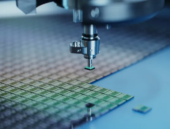
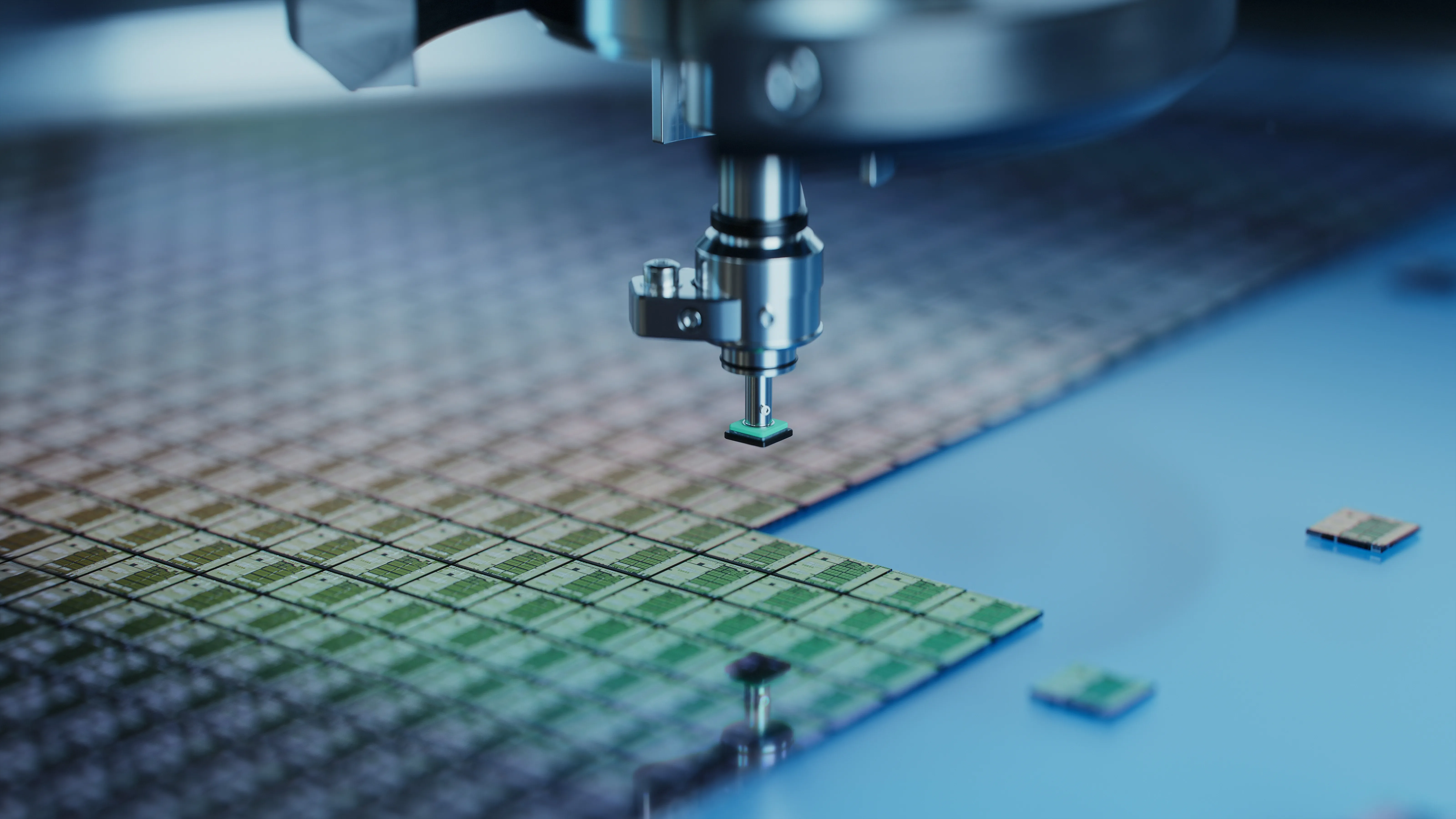
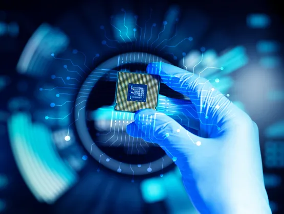
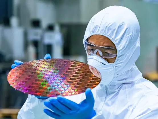
Integrated photonics offers the semiconductor industry a new way to increase the speed and capability of classical compute functions, as well as enabling quantum computing. The III-V Summit, hosted by SEMI Europe in partnership with Photon Delta at SEMICON Europa, opened with a compelling question: why is a photonics summit taking place in the middle of a semiconductor event? Ajit Manocha, President and CEO of SEMI, highlighted the growing convergence of the semiconductor and photonics industries, stating, “It is my firm belief that a boost to Moore’s Law will come from the III-V world.” Declaring that the rate of growth in integrated photonics is set to pick up substantially, Manocha assured, “I will be your ambassador to make sure that the III-V technologies gain far greater visibility than they have today.”Ajit Manocha, President and CEO, SEMIThe promise of new III-V technologies is generating significant excitement within the semiconductor industry. Abdul Rahim, Ecosystem Manager at PhotonWorld, acknowledged the reality that today’s III-V device industry operates in a limited sphere, stating, “The III-V world is still at the interface of industry and academia. There is one main application for III-V devices – transceivers for data centers.” Abdul Rahim, Ecosystem Manager, PhotonWorld Carlos Lee, Director General of the European Photonics Industry Consortium (EPIC), echoed this message, “Photonics is not so much an industry today; it’s an ecosystem. It lacks the standards, roadmaps, and market data that a full-fledged industry needs – but we are getting there.” Carlos Lee, Director General, European Photonics Industry Consortium (EPIC)However, Rahim pointed to a number of trends that are driving the growth of III-V technology for integrated photonics. One key development is large-scale integration, “over the years, the number of devices in one photonics integrated chip (PIC) has been growing fast, reaching tens of thousands of components on-chip,” Rahim explained. Additionally, the widening frequency range supported by III-V devices is unlocking new applications beyond the telecom sector. Broad Scope of Research into III-V Technology for Integrated PhotonicsResearch into III-V technology spans an impressive range of materials, processes and applications. Nick Singh, CTO at Compound Semiconductor Applications (CSA) Catapult, a government-backed technology incubator, described in detail the most important fields of research that are driving innovation in integrated photonics. “III-V materials are special because they can be engineered,” Singh explained. Highlighting their potential role in advancing quantum computing, Singh added, “The ability to use new materials is crucial to reducing the reliance on algorithmic compensation for errors and non-linearity in hardware.” Nick Singh, CTO, Compound Semiconductor Applications Catapult However, Singh emphasized the need for the photonics industry to address structural challenges that could hinder progress. “Collaboration is crucial to standardize process development kits (PDKs) for photonics device fabrication processes—it’s like the Wild West in PDKs right now,” Singh remarked. “Additionally, the availability of raw materials presents a significant challenge.”The truth of this warning was confirmed by Diane Scott, Vice President of TECHCET, stating, "The US has deemed gallium to be the number one supply chain risk among a list of 50 raw materials, and the European Union (EU) has identified gallium as a critical raw material."Diane Scott, Vice President, TECHCETSuch geopolitical concerns have done little to dampen the intensity of research in III-V technology. One of the powerhouses of integrated photonics research is IBM, and Heike Riel, a Fellow at IBM Research with a special interest in quantum computing, revealed promising avenues that IBM is exploring. “IBM has developed local III-V-on-silicon heteroepitaxy, “Riel explained. “Using a direct growth method, we can grow vertical, lateral, and even 3D structures in III-V, such as stacked GaAs structures.” Riel highlighted the potential applications of this technology in emerging processor designs, including the Artificial Intelligence Unit (AIU) and analog computing devices with in-memory logic. “Here, we can deploy GaAs as a photorefractive material, used as a grating, to perform the same function as conventional electronic non-volatile memory in an analog computer chip,” Riel noted. Heike Riel, IBM Fellow, IBM ResearchAlso at the forefront of photonics integration is Black Semiconductor, a start-up company based in Aachen, Germany, which is developing devices using graphene. Cedric Huyghebaert, CTO of Black Semiconductor, shared the company’s vision, “We want to use electronics to compute, and photonics to transfer data, and bring both functions together on the same chip.” Black Semiconductor’s mission is to become the first foundry to offer integrated graphene technology. “Our ambition is to integrate graphene in line with semiconductor standards using semiconductor tools – avoiding the need for exotic processing technologies,” Huyghebaert explained. “We also aim to demonstrate co-integrated photonics on a 300mm wafer system, regardless of the process node. In doing so, we want to prove that deep technological innovation of this kind is possible in Europe.”Cedric Huyghebaert, CTO, Black Semiconductor GmbH Bringing Integrated Photonics to the MassesAs III-V technology develops to enable a broader range of integrated photonics applications beyond the telecom market, experts are recognizing the need for it to become more accessible if it is to be adopted by a wider range of manufacturers. Joni Mellin, manager of the photonics business line at the X-Fab Group, emphasized, “As an industry, we need to bring electronics design automation (EDA) tools up to a level of capability that matches that of the silicon world, so that you do not need a PhD to do product design – we need to make it accessible to ordinary electronics engineers.” Joni Mellin, BL Manager Photonics, X-FAB GroupAdoption of the technology also requires access to production capacity. Peter Maat, Senior Product Manager at SMART Photonics, an open foundry for indium phosphide (InP) programmable interface controllers (PICs), highlighted the challenges in this area. Maat explained that the availability of the foundry as “not a trivial capability,” because many InP fabs are run by integrated device manufacturers, and are closed to other users. The SMART Photonics business model aims to provide a comprehensive enablement service for fabless manufacturing of PICs. “Our responsibility is to produce stable, manufacturable building blocks that we make available to designers and to provide a platform which enables our circuit building blocks to be combined into an integrated photonics circuit,” Maat said.Peter Maat, Senior Product Manager, SMART Photonics Jayakrishnan Chandrappan, Head of Advanced Packaging Technology at CSA Catapult, also emphasized the importance of access to production capability. “The CSA Catapult has one of the world’s only sub-10micron hybridization facilities for advanced packaging that is open to third-party users,” Chandrappan noted.Jayakrishnan Chandrappan, Head of Technology, Head of Technology - Advanced Packaging, Compound Semiconductor Applications CatapultPromising Future for Integrated PhotonicsAs the summit concluded, the atmosphere was charged with optimism about the future of integrated photonics. The discussions highlighted how III-V materials, combined with advanced packaging, are set to play a pivotal role in shaping next generation technologies. A recurring theme throughout the event was the profound impact III-V materials will have, as they poised to become a corner stone of virtually every emerging technological advancement. SEMI ContactLaith Altimime, President of SEMI EuropeEmail: [email protected]
Read More
With increasing demand for personalized smart devices, the MEMS and sensor market is undergoing rapid transformation. MEMS sensors are the backbone of smart wearable devices, seamlessly integrating multiple functions to monitor and simplify our day-to-day activities. As applications in healthcare, environmental tracking, and AR/VR expand, the need for ultra-compact, energy-efficient, and intelligent sensors is more critical than ever.In an exclusive conversation with SEMI, Stefan Finkbeiner, CEO of Bosch Sensortec, shared his perspective on the dynamic landscape of MEMS sensor technology. From Bosch’s evolution to a solutions provider with a focus on sustainability and market-driven innovations, Finkbeiner offered a deep dive into how Bosch Sensortec is positioning itself at the forefront of the industry. “We have to think in terms of the end application and determine what the right hardware and software configuration should be in order to provide solutions with the greatest benefit and flexibility.”Further insights into the future of MEMS and sensor technology will be shared by Finkbeiner during his keynote at the SEMI MEMS Imaging Sensors Summit on November 14, 2024, in Munich, Germany. Registration is still open.SEMI: Welcome, Stefan, and thank you for sharing your insights on advanced sensor technologies. Let’s start with a personal question: What motivates and inspires you about working in sensor technology?Finkbeiner: Sensor technology is very diverse and has significant impacts on consumers. We take pride in prioritizing consumers’ needs and benefits. True to the Bosch motto, “Invented for life,” we are committed to making life better, easier and healthier. This is demonstrated in our sensing solutions, which provide valuable data for fitness tracking in smartwatches, enhance the audio experience in hearables, and enable real-time monitoring of air quality to help individuals make informed decisions for a healthier environment. I am fascinated by technology advancements that are enabling the scaling of sensors—and the processing power and intelligence packed into these increasingly compact devices. For instance, our latest acceleration sensors for hearables are the smallest in the world and are nearly invisible at just 1.2 x 0.8 x 0.55 mm³.We leverage innovative wafer level chip scale packaging (WLCSP) to achieve this reduced form factor. These compact, feature-rich, high-performance accelerometers are easier to integrate in the latest generation consumer products where size and functionality are critical requirements.SEMI: How has Bosch Sensortec’s approach evolved over the years and what is the company’s primary focus today? Finkbeiner: We began our success story a few years ago as a hardware supplier, with one of our first applications being the 'Portrait-Landscape' function in smartphones. Over time, we’ve evolved into one of the leading providers of MEMS sensors.Today, we no longer see ourselves purely as a sensor manufacturer, but as a technology solutions provider. Our focus has shifted to think in terms of the end application and determine what the right hardware and software configuration should be to provide solutions with the greatest benefit and flexibility.Achieving this requires significant software and artificial intelligence (AI) development. In essence, we are optimizing software through self-learning models. Hardware remains essential for optimizing power consumption, with most sensors integrating a controller alongside the ASIC to enable seamless software integration.This unique software and hardware configuration unlocks exciting possibilities and broadens our market reach. We see significant growth in head-mounted devices, and we are actively working on related acoustics solutions.SEMI: Looking ahead, what trends do you anticipate will have the most significant impact on the MEMS sensors market?Finkbeiner: We see several trends that will significantly impact the MEMS sensor market. First, there is growing demand for personal health monitoring in consumer and mobile electronics. Wearable devices, in particular, are becoming essential tools for individuals to track their health and fitness status. This trend requires MEMS sensors to become even more accurate, with solutions that include sophisticated software algorithms to ensure reliability, accuracy, and reproducibility. As a result, AI and machine learning (ML) technologies will play a crucial role in enhancing sensor performance.A second important trend is the continued miniaturization of MEMS sensors. To meet customer demands, sensors must integrate more functionality, including edge-processing capabilities. For example, what once may have been a simple accelerometer with a step-counting algorithm is now evolving into a 6-axis Inertial Measurement Unit (IMU) with an integrated microcontroller and advanced AI/ML software. A great example of this is in True Wireless Stereo (TWS) earphones, where the IMU not only tracks steps but also enables complex tasks like dead reckoning and supports 3D audio—all within the tight constraints of a small TWS earbud housing. Low power consumption, as always, is a critical factor for these mobile devices to meet CE (Conformité Européenne) standards.Finally, we believe that smart glasses, augmented reality (AR) and virtual reality (VR) devices are poised to become the “next big thing.” These devices require advanced image projection optics that offer excellent optical quality, low weight, and ease of use to ensure consumer adoption. We believe our MEMS-based LBS (Laser Beam Scanning) solution is ideal for these applications. Additionally, the successful adoption of smart glasses hinges on high-performance MEMS sensors that are compact, accurate, and power-efficient—critical requirements for all-day wearability and functionality.These trends underscore the need for MEMS technology to evolve, integrating greater functionality, precision, and efficiency to meet the demands of next-generation consumer devices.SEMI: What are some of the biggest challenges facing the MEMS sensors industry today, and how can companies overcome them?Finkbeiner: One key challenge is that the smartphone market—arguably the most attractive market for a variety of MEMS and MOEMS sensors—has become more or less saturated. To stay competitive, MEMS companies must innovate existing products while also developing new, differentiated sensors and actuators for next-generation mobile products.SEMI: How is Bosch Sensortec supporting sustainability initiatives?Finkbeiner: We are helping to mitigate climate change with our low carbon footprint solutions.Up to 20% of annual global carbon emissions are caused by forest fires. This is equivalent to carbon dioxide emitted by all the vehicles driven worldwide. Our sensors can detect forest fires before they develop into wildfires by measuring various gases such as carbon monoxide and hydrogen. In parallel, we are working with our production partners to reduce our carbon footprint over the coming years, while also replacing or minimizing the use of environmentally hazardous chemicals, such as PFAS.SEMI: What are you most excited about for the MEMS Imaging Sensors Summit, and how do you think it will impact the European semiconductor industry?Finkbeiner: The European semiconductor industry has deep expertise in MEMS and sensor technologies, positioning it to make a significant impact in markets such as consumer health, optical sensing, and AR displays. By continuing to focus on sustainable solutions, we can drive even greater impact for the broader industry and secure Europe’s leadership in these growth sectors.I look forward to collaborating with industry peers at the Summit to define next steps needed to advance Europe’s leadership. The MEMS Summit is an invaluable opportunity to collaborate and drive progress, and I warmly invite my colleagues to join us in shaping the future of the European semiconductor industry.Dr. Stefan Finkbeiner Dr. Stefan Finkbeiner has been CEO and General Manager at Bosch Sensortec GmbH since 2012. He was born in 1966 in Freudenstadt, Germany. Stefan Finkbeiner held various senior positions at Bosch including Director of Sensor Marketing, Director of Corporate Research in microsystems technology, and Vice President of Sensor Engineering. He looks back on almost 30 years in semiconductor industry working in different positions related to sensor research, development, manufacturing, and marketing. Due to his wide experience in semiconductor and sensor industry, Stefan Finkbeiner is a recognized guest in panel discussions and as keynote speaker. SEMI ContactSitong He / Communications Manager, SEMI EuropeEmail: [email protected]: +49 151 5546 2638
Read More
In today’s rapidly evolving semiconductor industry, ensuring both precision and efficiency in manufacturing has become an increasing challenge, particularly as advanced technologies like MEMS and AI chips push the boundaries of design and production. Inspection methods that were once sufficient are now falling short, making room for cutting-edge solutions powered by artificial intelligence (AI). The introduction of AI-driven 3D X-ray inspection technologies is transforming the landscape, offering manufacturers a sophisticated tool to ensure quality control, while driving sustainable production strategies.SEMI spoke with, Joscha Malin, Product Manager, and Daniel Stickler, R D Expert for X-ray Imaging at Comet AG, Industrial X-Ray System Division, to explore how AI-powered 3D X-ray inspection technologies are shaping manufacturing. They delve into how these technologies address critical challenges during inspections and defect analysis, using tools such as Dragonfly 3D World software for user-friendly, AI-driven insights that facilitate effective decision-making.Further insights into the application of AI-powered 3D X-ray inspection technologies and their role in advancing MEMS manufacturing will be presented by Stickler at the SEMI MEMS Imaging Sensors Summit on November 14, 2024, in Munich, Germany. Registration is now open.SEMI: Thank you both for agreeing to share your insights. To start, can you explain the importance of inspection strategies in the context of MEMS manufacturing?Malin: As MEMS devices become increasingly miniaturized and complex, effective inspection strategies are crucial. These strategies not only accelerate the wrap-up of production processes, but also significantly enhance product yield. With tighter tolerances and various materials involved, ensuring the integrity and functionality of each component is more critical than ever. A robust inspection strategy allows us to catch potential defects early, which can save time and costs associated with rework or scrap.Stickler: The evolution of MEMS technology, particularly in AI chips, demands a higher level of inspection sophistication. Traditional methods may fall short in providing the necessary detail and speed, which is why we’re focusing on advanced solutions like our AI-powered 3D X-ray inspection.SEMI: Could you elaborate on how the 3D X-ray technology differs from conventional inspection methods? Stickler: The 3D X-ray technology we utilize acts as a bridge between traditional optical methods and standard 2D X-ray inspection. It offers high-resolution, three-dimensional images without damaging the samples. 3D X-ray technology emphasizes three main benefits: clarity, efficiency, and actionable insights. This means we can obtain detailed images that help us analyze components more effectively, allowing for real-time decision-making.Malin: Moreover, the clarity and detail provided by the 3D X-ray images are critical when it comes to defect analysis in MEMS devices. They allow us to assess mechanical, electrical, and assembly errors in ways that conventional methods simply cannot. This leads to a more reliable production process.SEMI: What specific MEMS defects can be effectively analyzed using this technology?Stickler: There are several types of defects we can analyze. For instance, we can detect mechanical defects such as stiction or fractures, as well as electrical failures like short circuits. The 3D X-ray inspection allows us to visualize these defects in detail. Additionally, we can monitor assembly errors, which are particularly important in complex MEMS devices where misalignments can lead to significant issues.Malin: I’d like to add that early detection of these defects is paramount. The faster we identify issues, the quicker we can implement corrective actions, thereby improving overall yield and reducing production costs.SEMI: You mentioned yield improvement earlier. Can you explain how your technology contributes to that?Malin: Our approach supports process optimization by providing information on product characteristics and, for example, allows us to identify trends early on that may lead to yield issues later. We also aim to accelerate new product introduction in the early phase by rapid feedback, saving time and cost. This is crucial because many defects may not be apparent until later stages of production. With our technology, we can monitor samples in real-time, allowing us to react promptly to emerging challenges.Stickler: By integrating this feedback loop, we can significantly shorten the time to market for new products. This is particularly beneficial in industries where speed and efficiency are essential.SEMI: Can you tell us about Dragonfly 3D World software and its role in this process?Malin: Dragonfly 3D World is a user-friendly software that leverages AI and, specifically, deep learning for image processing. It enables users to efficiently perform bump metrology and defect identification, for example, without needing extensive expertise in the field. The software makes complex processes manageable, even for operators who may not be specialists in image processing.Stickler: Beside MEMS and advanced packaging in GPU production, this software is indeed an “AI-for-AI” application. By utilizing deep learning, users can train models that adapt to various imaging tasks, making the entire inspection process more efficient. The insights generated from the 3D X-ray images are automated, enhancing usability and streamlining workflows.SEMI: In conclusion, what are the key takeaways you’d like to share?Malin: The key takeaways are that AI-driven 3D X-ray inspection is transformative for the MEMS manufacturing process, enhancing inspection strategies and defect detection significantly. By integrating advanced technologies, we can ensure higher product quality and efficiency.Stickler: Yes, and I would emphasize the importance of powerful monitoring and non-destructive test tools. Our innovative solutions not only improve yield, but also pave the way for sustainable practices in manufacturing, ultimately benefiting the industry. Dr. Daniel SticklerDirector X-ray Technology Components at Comet AG, Industrial X-Ray System Division. Based in Hamburg, Germany, he holds a PhD in Physics from the University of Hamburg and has extensive experience in X-ray imaging, semiconductor X-ray applications and product innovations. Joscha MalinDirector Product Marketing Software Products at Comet AG, Industrial X-Ray System Division. Based in Hamburg, Germany, he holds a degree in Electrical Engineering with specialization in Semiconductors and profound experience in the industry. For over a decade, he has focused on developing X-ray inspection and metrology solutions, especially for the Semiconductor industry. SEMI ContactSitong He / Communications Manager, SEMI EuropeEmail: [email protected]: +49 151 5546 2638
Read More