downloadGroupGroupnoun_press release_995423_000000 copyGroupnoun_Feed_96767_000000Group 19noun_pictures_1817522_000000Member company iconResource item iconStore item iconGroup 19Group 19noun_Photo_2085192_000000 Copynoun_presentation_2096081_000000Group 19Group Copy 7noun_webinar_692730_000000Path
Skip to main content
Default Banner Image

South Korea

Registration

Registration

Early-bird Registration Close: Friday, May 24 / 5:00pm in KST

[Early Bird]

· SEMI Member: KRW 308,000
· Non-Member: KRW 363,000

[Regular]

· SEMI Member: KRW 385,000
· Non-Member: KRW 385,000


※ Registration fee includes lunch and reception.

Registration
South Korea Registration SMC-Korea-2024-Banners-squre.jpg Business Technical

OVERVIEW

  • Date: May 29(Wed), 2024
  • Time: 09:00 - 18:30
  • Venue: Convention Hall 2, 3F, Suwon Convention Center


NOTICE

  • Simultaneous interpretation will be provided
  • Presentation files agreed by speakers will be provided to attendees.


SPONSORS

SMC-Korea-2023-Sponsor_DW.jpg SMC-Korea-2023-Sponsor_DP.jpg SMC-Korea-2023-Sponsor_JSR.jpg SMC-Korea-2023-Sponsor_ET.jpg
SMC-Korea-2023-Sponsor_DS_0.jpg Air LiquideHuntsman
 
line_2.jpg


CONTACT

Convention Hall 2, 3F, Suwon Convention Center
Suwon-si
Gyeonggi-do
South Korea
10:00 am - 10:05 am
 Hyun-Dae (H. D.) Cho - President, SEMI Korea
HD Cho
President
SEMI Korea

Welcome

10:05 am - 10:35 am
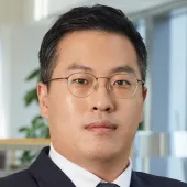
seongtae oh
Seong Tae Oh
Fellow
TEL

Process Technologies for Continuous Scaling of Logic Devices

The rapid growth of AI, big data, IoT, and 5/6G communication necessitates the sophisticated computing power and efficiency of semiconductor devices, driving demand for various components such as HPC, GPU, ASIC, FPGA, and HBM. Semiconductor device and equipment industries are also challenging various new technologies to accommodate such diversifying applications and proceed with sustainable development in the era of AI and ICT.
According to the roadmap over the next 10 years, semiconductor technologies are expected to develop into the scaling technologies to further extend the existing Moore's Law and hybrid device technologies that integrate legacy nodes and advanced nodes into one. Therefore, in this presentation, we will look at the latest logic technology roadmap and introduce new process technologies to implement it.

※ Biography

10:35 am - 11:00 am
Wonho Yeon
Wonho Yeon
Research Fellow
KIEP

Supply Chain Management

11:00 am - 11:25 am
Mark Thirsk
Mark Thirsk
Managing Partner
Linx Consulting

Localization Challenges of the Materials Supply Chain

11:25 am - 11:50 pm
Stefan CHITORAGA
Stefan CHITORAGA
Technology and Market Analyst- Packaging & Assembly
Yole Group

Material Trends in Advanced Packaging & Power Module Packaging (video recording)

11:50 am - 1:00 pm

Lunch

1:00 pm - 1:25 pm
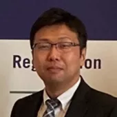
Dr. Montray C. Leavy
Montray C. Leavy
Deputy CTO
Entegris

Materials Innovation Advancing the Angstrom Era

Materials innovation within the Semiconductor industry has been a driving force since the planar 2D MOSFET to the current 3D gate-all-around (GAA) transistor architectures and will continue its criticality as we embark on 500-layer flash memory designs and Angstrom level critical interconnect dimensions. To achieve these once incomprehensible levels of lateral and vertical scaling, device design engineers and manufacturers are increasingly relying on disruptive materials innovation to enable the density and performance gains required at each successive technology node. As the performance requirements for the most advanced devices become more challenging, materials have shown to have an increased contribution to device performance over scaling and design. This has led to a greater portion of the periodic table being incorporated into semiconductor processing.

The integration of new materials, such as novel photoresists, interconnect metals & alloys, ultra-pure polymers, chemically modified polymer membranes, and formulated chemicals, into the chip fabrication increases process complexity and makes yield ramps more challenging. With more process steps in the overall device build, speed to yield and process integrity are more critical than ever to achieve technology qualification schedules. This presentation will focus on Entegris’ approach to materials innovation, the integration of these novel materials coupled with co-optimized solutions enabling industry technology roadmaps and yield requirements while preserving integrity of delivery and process control.
※ Biography

1:25 pm - 1:50 pm
Sadaaki Katoh
Sadaaki Katoh
JOINT2 Team Manager
Resonac

Advanced Packaging Materials and Evaluation Platform at Resonac

Resonac has started Packaging Solution Center as new R&D center to propose one-stop solution for customers in 2018 and established the co-creative packaging evaluation platform “JOINT2” with leading companies to accelerate the development of advanced materials, equipment and substrates for 2.xD and 3D package in October, 2021.

2.xD and 3D packages require to connect chips and components in high density, therefore, both wiring pitch and vertical interconnect dimension must be finer and finer. At the same time, in order to achieve better performance, more and more chips are integrated together and thus the package size is increasing. To meet these requirement, we are developing fine vertical/lateral interconnect technology and the study of fabrication and reliability for the extremely large 2.5D advanced package.
The presentation will cover the significance and strengths of JOINT2, and updates on research and development.

※ Biography

1:50 pm - 2:15 pm
seonjun heo.png
Seongjun Heo
Process Engineering Director
Lam Research

Dry Resist for Holistic EUV Patterning

EUV lithography infrastructure has become the critical element of semiconductor industry to enable the device scaling down. It consists of not only light source, optical system but also masks, photoresist. The EUV stochastic effects present challenges to optimizing EUV resist resolution, line edge roughness, and sensitivity simultaneously. To overcome these challenges, Lam introduced the new dry resist combined with the new dry development technology.

Lam’s EUV dry resist, coupled with ASML’s EUV scanners and Lam’s holistic patterning solutions, will extend the patterning roadmap (Moore’s Law) for the next 10 years and beyond by offering a high-resolution, high-fidelity, defectivity-free, and greener solution for ≤32nm pitch L/S, and ≤40nm pitch pillar and contact hole EUV patterning in the fab. EUV dry resist technology also has been validated demonstrating superior dose-to-defectivity for <32nm pitch L/S, well suited for logic applications. Lam’s EUV dry resist is uniquely suited for future HiNA EUV patterning thanks to robust resist thickness scaling while maintaining high etch selectivity and high contrast.

※ Biography

2:15 pm - 2:30 pm

Break

2:30 pm - 2:55 pm
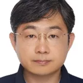
김용성
Yongsung Kim
TL
SK hynix

Sustainability Challenges of the Semiconductor Industry

As demand for chips surge, the semiconductor industry is struggling to reduce its environmental footprint. While the environmental impacts of semiconductor (and electronic products that depend on them) have mostly been liked to ‘manufacturing’ and ‘use’ phases of products which consume a significant amount of water and energy, the attention is shifting to the 'material extraction’ and ‘end-of-use’ phases of products following concerns over the e-waste issue. In this presentation, I will focus on the latest findings of the global e-waste challenge, what this means from the materials perspective, and its implications to product design and manufacturing. I will also introduce SK hynix's strategy and targets towards improving the circularity of products, and our partnership with customers/vendors to achieve a common goal.
2:55 pm - 3:20 pm
Eun-Ho Sohn
Eunho Sohn
Head of Interface Materials and Chemical Engineering Research Center
KRICT

Trends in Regulation of PFASs (per- and polyfluoroalkyl substances) and Technological Development Strategies

Fluorine compounds exhibit exceptional physical properties that set them apart from other organic materials. Consequently, they have been utilized as core materials to enhance the functionality, performance, and value of products across various key industries including electrical and electronics, semiconductors, displays, and automobiles.
However, on March 22nd of last year, the European Chemicals Agency (ECHA) issued a report imposing restrictions on the usage of over 10,000 types of per- and polyfluoroalkyl substances (PFASs) across all industries, sparking significant upheaval within the sector.
In this presentation, we will learn in detail about the definition of PFAS, and the content, progress, and schedule of PFAS regulations in Europe and the United States, and contemplate the direction of future technology development.

※ Biography

3:20 pm - 3:45 pm
김광섭
Karl Kim
APAC Semiconductor Marketing Manager
Syensqo

Sustainability Opportunities for A Diverse and Secure Fluorinated Material Supply Chain

As semiconductors become more advanced and the fabrication processing conditions more extreme, the essentiality of a sustainable and secure fluorinated material supply chain plays a vital role in the future of semiconductor manufacturing. The principles of developing this supply chain are directly aligned to support the sustainability and emission roadmaps of the semiconductor industry. Syensqo will introduce the following content:
1) Priorities when Specifying Materials for a Sustainable Supply Chain
2) The Key to Sustainability - Application Segmentation
3) Case Studies

※ Biography

3:45 pm - 4:10 pm
dupont_Jae Hwan Sim
Jae Hwan Sim
R&D manager/Korea R&D EUV team leader
DuPont

Innovating Safe and Sustainable by Design: Strategies and Steps toward Reduction of Substances of Concern in Photolithography Materials

Growing scientific evidences suggest that certain per- and polyfluoroalkyl substances (PFAS) pose global environmental and health risks. In response, global governments are contemplating measures to limit the use of these chemicals in various industries. However, specific types of PFAS are indispensable and no substitutes are currently available for most chip manufacturing applications in the semiconductor industry. Aligned with the objective of Safer and Sustainable by Design, DuPont has launched a comprehensive program to reduce PFAS usage in photoresist and associated lithography materials. In this presentation, we will provide an overview of DuPont's innovative initiatives and technical challenges encountered in this endeavor.

※ Biography

4:10 pm - 4:35 pm
Floris Buijzen
Floris Buijzen
Senior Director Product Management
Corbion

CORBION: PURASOLV® ELECT for a more Sustainable Semiconductor Manufacturing

Solvents are used extensively in the semiconductor manufacturing process. Solvents are estimated to be responsible for around 7% of the Scope 3 emissions of the semiconductor industry. The typical solvents that are used are produced from fossil resources and with that not in line with net zero ambitions. For more than 20 years Corbion has been supplying biobased ethyl lactate to the semiconductor industry under it’s brand name PURASOLV® ELECT, meeting the stringent requirements of the industry. Typical applications are photoresist for i/g-line / KrF / ArF / EUV, RRC, Edge bead removal and as thinner. Biobased ethyl lactate is sustainable and safe by design: it is produced from renewable resources, non-toxic and safe to workers, biodegradable and offers a significant carbon footprint reduction compared to incumbent solvents. Switching to biobased ethyl lactate thus enables more sustainable semiconductor manufacturing.

※ Biography

4:35 pm - 4:50 pm

Break

4:50 pm - 5:20 pm
ki ill moon
Ki-Ill Moon
VP
SK hynix

Technology and Future of Semiconductor Packaging Materials

The technological advancement of semiconductor materials is a key factor along with the technological advancement of the process. And recently, the importance of Advanced PKG is increasing, and SK Hynix has achieved the result of improving product performance by developing MR-MUF materials. This proves the importance of materials. In the future, there are more packaging challenges for high-speed memory products such as HBM, and I plan to announce Need for material development to satisfy them.

※ Biography

5:20 pm - 5:50 pm
Seongjun Park
Sungjun Park
Executive Vice President and Head of Material Development Team
Samsung Electronics

Big Challenges for Small Worlds

The number of transistors in semiconductor chip has been increased twice every two years for more than 50 years, following the famous Moore’s Law and somehow, it was taken to be granted. In reality, it was a big accomplishment with an unimaginable amount of efforts and collaborations, including the development of new materials.

New material has been developed and introduced to improve the performance and capacity of electronic devices through smaller design rules. New Photo Resists (PR) for higher resolution with smaller defects and higher uniformity were developed. And Precursors were also developed to meet the process challenges for the smaller design rules, such as higher aspect ratios. High etch selective Etchant and CMP Slurry with low scratch were requested. And the requirements in new materials are getting tougher and stronger with the evolution of AI, which needs more computing power than ever. Even materials that has never been expected in industry and has been studied only in academia are being actively considered.

Even the worse, the surrounding situation for material development and manufacturing is getting tougher. Environmental regulations are getting tighter. Gases with high global warming potential were begun to be replaced. Recently, EU announced banning PFAS materials in near future and US raised bars for PFAS materials. And carbon zero policy is coming to us slowly but firmly.

In this talk, we will discuss the current status and future direction of material research. We will discuss the development directions to improve the performance of devices and to consider environmental regulations. And we will discuss the virtue of working together as a big one-team to overcome all the obstacles mentioned above in the world of extreme technology.

※ Biography

5:50 pm - 6:30 pm

Networking Reception

EMG

Materials Resilience: Navigating Challenges, Embracing Opportunities

Currently, sustainablility and efficiency of global supply chains are becoming more critical to the semiconductor industry. Global political tensions are affecting the semiconductor market, which is further revealing the vulnerabilities of the supply chain. In addition, ongoing environmental regulations are also having an increasing impact on the industry. The growing demand for eco-friendly products and manufacturing processes puts companies under pressure to introduce innovative technologies and solutions along with this regulatory compliance.
These trends present new challenges and opportunities for the semiconductor industry. SMC Korea reflects these issues and discusses current market conditions and future prospects. Through this conference, we expect major companies and experts will be able to share their experiences and knowledge, find innovative solutions together, and explore the future of the industry together. Don't miss these up-to-date discussions presented by global experts.


10:00 am - 6:30 pm Off Add to Calendar 2024-05-29 10:00:00 2024-05-29 18:30:00 SMC Korea 2024 Materials Resilience: Navigating Challenges, Embracing OpportunitiesCurrently, sustainablility and efficiency of global supply chains are becoming more critical to the semiconductor industry. Global political tensions are affecting the semiconductor market, which is further revealing the vulnerabilities of the supply chain. In addition, ongoing environmental regulations are also having an increasing impact on the industry. The growing demand for eco-friendly products and manufacturing processes puts companies under pressure to introduce innovative technologies and solutions along with this regulatory compliance.These trends present new challenges and opportunities for the semiconductor industry. SMC Korea reflects these issues and discusses current market conditions and future prospects. Through this conference, we expect major companies and experts will be able to share their experiences and knowledge, find innovative solutions together, and explore the future of the industry together. Don't miss these up-to-date discussions presented by global experts. Convention Hall 2, 3F, Suwon Convention Center Suwon-si Gyeonggi-do South Korea SEMI.org [email protected] Asia/Seoul public Asia/Seoul

WILMINGTON, Del., Feb. 29, 2024 — DuPont (NYSE: DD) today announced that Jon Kemp, President, DuPont Electronics & Industrial, has been named Chair of the Board of Industry Leaders of SEMI, a global industry association serving the electronics design and manufacturing supply chain.

The Board of Industry Leaders provides strategic guidance and direction for key global SEMI initiatives and programs – including sustainability, workforce development, supply chain management, and global advocacy – to address semiconductor industry challenges and advance its growth. The Board comprises executive-level thought leaders representing the diversity of SEMI membership. As Chair, Kemp will lead the Board in its work, which also includes identifying emerging technology and business issues where SEMI can build impactful member value for the future.

“Jon is already a valued contributor to the SEMI International Board of Directors in its fiduciary role, and we are pleased to have him stepping up to chair our Board of Industry Leaders to make sure our members’ voices and needs are reflected across the diverse range of our programs and initiatives,” said SEMI President and CEO Ajit Manocha. “We look forward to working with Jon to address some of the global semiconductor industry’s toughest challenges, such as our talent gap, and empowering the industry’s continued growth and innovation.”

As President of DuPont’s Electronics & Industrial business, Kemp leads the organization in serving the semiconductor, circuit board, display, digital and flexographic printing, healthcare, aerospace, defense, industrial and transportation industries. Kemp has more than 20 years of experience in the electronics industry and strategic leadership, including his service on the SEMI International Board of Directors since 2016.

“I’m honored to be part of this group of industry leaders who are tackling some of the most critical issues facing the semiconductor industry that no single company or organization can solve alone, like sustainability, government advocacy, workforce development, and supply chain management,” said Kemp. “There’s tremendous value in collaborating across industries and I look forward to what we’ll achieve together across the semiconductor ecosystem.”

About SEMI
SEMI® is the global industry association connecting over 3,000 member companies and 1.5 million professionals worldwide across the semiconductor and electronics design and manufacturing supply chain. We accelerate member collaboration on solutions to top industry challenges through Advocacy, Workforce Development, Sustainability, Supply Chain Management and other programs. Our SEMICON® expositions and events, technology communities, standards and market intelligence help advance our members’ business growth and innovations in design, devices, equipment, materials, services and software, enabling smarter, faster, more secure electronics. Visit www.semi.org, contact a regional office, and connect with SEMI on LinkedIn and X to learn more.

About DuPont Electronics & Industrial
DuPont Electronics & Industrial is a global supplier of new technologies and performance materials serving the semiconductor, circuit board, display, digital and flexographic printing, healthcare, aerospace, industrial, and transportation industries. From advanced technology centers worldwide, teams of talented research scientists and application experts work closely with customers, providing solutions, products and technical service to enable next-generation technologies. http://electronics.dupont.com

About DuPont
DuPont (NYSE: DD) is a global innovation leader with technology-based materials and solutions that help transform industries and everyday life. Our employees apply diverse science and expertise to help customers advance their best ideas and deliver essential innovations in key markets including electronics, transportation, construction, water, healthcare and worker safety. More information about the company, its businesses and solutions can be found at www.dupont.com/. Investors can access information included on the Investor Relations section of the website at investors.dupont.com.

Belgium France Germany Ireland Italy Japan Malaysia Singapore South Korea Taiwan United States Vietnam 360x317_Event_Calendar_Ad_SURoadmap_v6@2x (1).png Business Featured Speakers
Highlighted content

SEMI University celebrates its first anniversary! Our pledge remains unwavering: providing comprehensive, technical education to equip you with the skills needed for a prosperous journey in the semiconductor sector.

Are you ready to take your semiconductor industry knowledge to the next level? We're thrilled to invite you to our upcoming webinar titled "SEMI University - Introduction and 2024 Roadmap." This webinar promises to be an informative session where you'll gain insights into the latest updates, exciting live trainings, new certifications, and courses offered by SEMI U in 2024.  

During this webinar, you can expect to:  

  • Discover the latest updates and enhancements to SEMI U's course catalog.  
  • Learn about the exciting live, in-person training courses scheduled for spring of 2024.  
  • Get insights into new certifications and courses designed to keep you ahead in the industry.  
  • Gain access to a special 10% discount on ALL courses.  

Choose your session:

United States

Naresh Naik
Naresh Naik
Director, SEMI University
SEMI
Workforce Development

Join us to discover our current course offerings, upcoming additions, new certifications, and more! Engage in a Q&A session. Plus, by attending this free webinar, you'll receive a 10% discount code for all our courses.

Off Add to Calendar 2024-03-19 00:00:00 2024-03-19 00:00:00 SEMI University - Introduction and 2024 Roadmap Join us to discover our current course offerings, upcoming additions, new certifications, and more! Engage in a Q&A session. Plus, by attending this free webinar, you'll receive a 10% discount code for all our courses. United States SEMI.org [email protected] America/Los_Angeles public
Event format

WILMINGTON, Del., Jan. 22, 2024 — DuPont (NYSE: DD) today announced that Drew Chambers has been named global business director, Lithography Technologies business in DuPont Electronics & Industrial, effective Jan. 1. Chambers succeeds George Barclay, Ph.D., who has elected to retire after more than 25 years of service.

“George Barclay’s significant contributions to our lithography business and portfolio have been tremendous and we are grateful for the lasting legacy he leaves with our organization,” said Sang Ho Kang, VP & General Manager, Semiconductor Technologies, DuPont Electronics & Industrial. “A true technical expert, George is a prolific innovator and visionary leader.”

“Drew Chambers has demonstrated outstanding leadership across multiple technology segments in electronics and is a strong proponent of delivering results to meet the needs of our customers,” said Kang. “In his new role as the leader of our lithography materials portfolio, Drew will play a pivotal role in furthering our offerings for extreme ultraviolet lithography and other advanced patterning solutions.”

Chambers brings a diversity of experiences both at DuPont and elsewhere in the electronics industry. He joined DuPont in 2019 as global marketing director for chemical mechanical planarization (CMP) pads in CMP Technologies and most recently served as acting business director. Prior to DuPont, he led the Electronics & Surface Technologies segment for Ferro Corporation, led regional sales and marketing for ESL ElectroScience (now part of Ferro Corporation), and worked in new business development for Lutron Electronics. Earlier in his career, Chambers held several roles in engineering, product management and account management in the semiconductor materials segment with Rohm and Haas Electronic Materials (now part of DuPont). Chambers holds an MBA from Duke University’s Fuqua School of Business and a BS in chemical engineering from Lafayette College.

DuPont Lithography Technologies is a global leader in materials for microlithography, with offerings enabling advanced patterning at the most advanced technology nodes; and bringing quality, yield and defectivity improvements to existing lithography processes. DuPont’s portfolio includes ArF photoresists, KrF photoresists, i/g line photoresists, extreme ultraviolet (EUV) photoresists, advanced overcoats, EUV underlayers and anti-reflective coating materials. Lithography Technologies is part of Semiconductor Technologies in DuPont Electronics & Industrial.

About DuPont Electronics & Industrial
DuPont Electronics & Industrial is a global supplier of new technologies and performance materials serving the semiconductor, circuit board, display, digital and flexographic printing, healthcare, aerospace, industrial, and transportation industries. From advanced technology centers worldwide, teams of talented research scientists and application experts work closely with customers, providing solutions, products and technical service to enable next-generation technologies. http://electronics.dupont.com

About DuPont
DuPont (NYSE: DD) is a global innovation leader with technology-based materials and solutions that help transform industries and everyday life. Our employees apply diverse science and expertise to help customers advance their best ideas and deliver essential innovations in key markets including electronics, transportation, construction, water, healthcare and worker safety. More information about the company, its businesses and solutions can be found at www.dupont.com. Investors can access information included on the Investor Relations section of the website at investors.dupont.com.

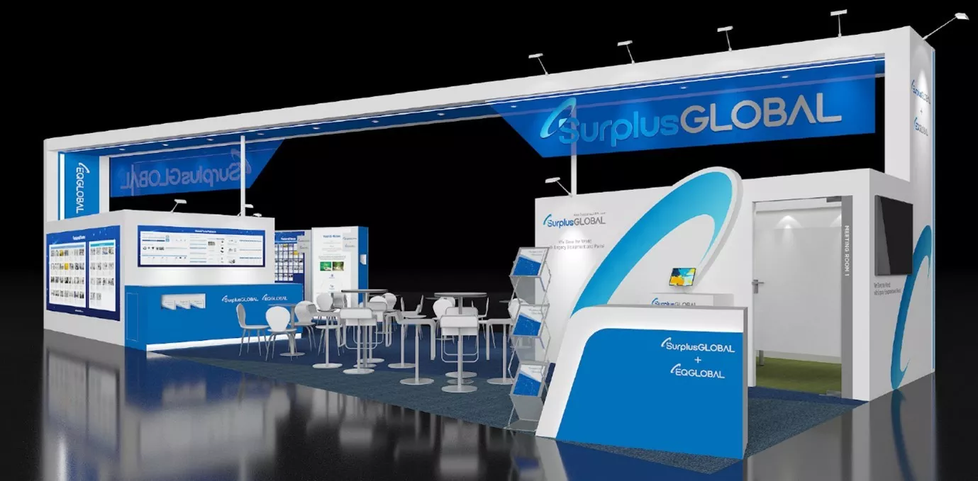
Semiconductor equipment platform company SurplusGLOBAL has announced its participation in the SEMICON KOREA 2024 exhibition, in collaboration with its subsidiary EQ GLOBAL. The SEMICON KOREA 2024 exhibition, which commenced in 1987, stands as a prominent event for the South Korea semiconductor industry, showcasing the latest semiconductor materials, equipment, and related technologies. The event also encompasses a semiconductor technology symposium, market trend forums, and purchase consultation sessions. This year is scheduled to take place from January 31 to February 2 at COEX in Seoul, with approximately 500 companies expected to participate.


[Photo: SurplusGLOBAL booth at SEMICON KOREA 2024 exhibition]


Bruce Kim, CEO of SurplusGLOBAL, stated, "We are accelerating our global network expansion, with a presence now established in Mainland China, the United States, Japan, Taiwan(China), and Singapore. Our business is evolving beyond the focus on legacy semiconductor equipment distribution to include refurbishing, manufacturing, and parts production and distribution." He continued, "Our Global Parts Platform business, leveraging South Korea's semiconductor equipment parts infrastructure, provides repair, manufacturing, and services to global semiconductor companies. This expansion is fueled by the increasing market demand. Currently, we serve over 50 companies, supplying obsolete parts. Recently, we facilitated prompt recovery by delivering urgent parts to Japanese semiconductor fabs affected by an earthquake. Additionally, we are actively developing e-commerce through 'Global Parts Platform: Marketplace,' with plans to introduce AI-based personalized recommendation services by the end of this year."
SurplusGLOBAL will be located at booth DS30 in Hall D at SEMICON KOREA, participating as a joint exhibitor with its subsidiary EQ GLOBAL. The company plans to showcase Head Motor components used in RF generators and CMP (Chemical Mechanical Polishing) equipment, along with repair services.
In December of last year, SurplusGLOBAL was selected by the Ministry of Employment and Labor as a 'Great Workplace for Youth.'


Lansdale, PA – Greene Tweed, a leading global manufacturer of high-performance sealing solutions and engineered components, announces the introduction of Fusion® F07, a performance-enhanced fluoroelastomer. Developed by Greene Tweed material scientists and application engineers, Fusion® F07 is specifically crafted to withstand common Etch and CVD oxygen/fluorine based gases in semiconductor processing subfab lines, at temperatures up to 355°F (180°C).

With an expected lifetime of at least 6 months, Fusion® F07 lasts longer than standard FKM in subfab vacuum system lines. As a result, the new performance enhanced FKM extends the time between planned maintenance activities. Notably, it provides a better total cost of ownership where applications do not require an FFKM compound.

“At Greene Tweed, we enable customers to operate efficiently and safely in the world’s most demanding environments. We understand that the semiconductor industry needs reliability and longevity. Fusion® F07 is a result of meticulous research and development, aimed at not only extending the life of their system but also improve operational efficiency,” says Magen Buterbaugh, President and CEO, Greene Tweed.

Fusion® F07 can be purchased as a seal assembly or as an individual O-Ring. Customers can effortlessly upgrade to Fusion® F07 and experience the benefits of extended lifetime and the resultant reduced operating costs as the seals are form-fit replaceable with other industry standard (KF/ISO flange fittings) seals. A blue outer ring allows for easier identification upon installation and replacement. Fusion® F07 seals are available in most typical sizes, including KF16, KF25, KF40, KF50, ISO63, ISO80, ISO100, ISO160, and ISO200.

About Greene Tweed
As a leading global provider of sealing solutions to the semiconductor industry for over four decades, Greene Tweed engineers advanced elastomer seals and thermoplastic components that are found in a broad range of mission-critical equipment in key process areas of the world’s semiconductor fabs, including etch, deposition, aqueous, and electro-chemical (electroplating). The company is now investing in Korea with its upcoming state-of-the-art manufacturing facility expected to commence production this year. “Greene Tweed has a history of investing to meet the demands of our global customers and the Korea expansion offers the organization an opportunity to support the continued growth of the semiconductor industry in the region. The multi-million-dollar investment represents a significant increase in the company’s global manufacturing capacity while enabling supply chain resiliency,” said Magen Buterbaugh.

Reaffirms Full Year 2023 Revenue Expectations Above $1.1 billion

BEVERLY, Mass., Jan. 16, 2024 -- Axcelis Technologies, Inc. (Nasdaq: ACLS), a leading supplier of enabling ion implantation solutions for the semiconductor industry, today increased financial guidance for the fourth quarter of 2023 and reaffirmed its expectations for the full year. Based on preliminary fourth quarter financial results, the Company expects revenue for the fourth quarter of 2023 to be greater than $300 million, above the approximately $295 million prior guidance, and reaffirmed its expectation for full year 2023 revenue above $1.1 billion. Earnings per diluted share for the fourth quarter of 2023 are now forecasted to be greater than $2.05, above prior guidance of approximately $2.00.

President and CEO Russell Low commented, “Our excellent financial performance in the fourth quarter and for the full year 2023 resulted from strong execution by Axcelis employees, combined with our leadership position in the growing power device market.” Low continued, “Based on our strong yearend backlog and fourth quarter bookings, especially in power devices, we expect the power device market to remain healthy in 2024. We also believe that the mature process technology and memory segments, two markets in which Axcelis is well-positioned, will recover in the second half of the year, enabling strong growth in 2025.”

James Coogan, executive vice president and chief financial officer said, “We look forward to discussing our results for 2023 and expectations for 2024 on our upcoming fourth quarter and full year earnings call. We believe we are still on track to achieve our $1.3 billion revenue model in 2025. This expectation is based on continued demand for the Purion product family, continued bookings strength, and a backlog stretching into 2025.” Coogan continued, “Additionally, we continue to manage spending to improve our earnings power and to invest in R&D to strengthen our market position.”

Fourth Quarter and Full Year 2023 Conference Call
The Company will release financial results for the fourth quarter and full year 2023 on Wednesday, February 7, 2024, at 4:00 p.m. Eastern Time (ET). The Company will host a call to discuss the results for the fourth quarter and full year 2023 on Thursday, February 8, 2024, at 8:30 a.m. ET. The call will be available to interested listeners via an audio webcast that can be accessed through the Investors page of Axcelis' website at www.axcelis.com, or by registering as a Participant here https://edge.media-server.com/mmc/p/su3u4oev. Webcast replays will be available for 30 days following the call.

Safe Harbor Statement
This press release contains forward-looking statements under the SEC safe harbor provisions. These statements, which include our guidance for future financial performance, are based on management’s current expectations and should be viewed with caution. They are subject to various risks and uncertainties, many of which are outside the control of the Company, including the timing of orders and shipments, the conversion of orders to revenue in any particular quarter, or at all, the continuing demand for semiconductor equipment, relative market growth, continuity of business relationships with and purchases by major customers, competitive pressure on sales and pricing, increases in material and other production costs that cannot be recouped in product pricing and global economic, political and financial conditions. These risks and other risk factors relating to Axcelis are described more fully in the most recent Form 10-K filed by Axcelis and in other documents filed from time to time with the Securities and Exchange Commission.

About Axcelis
Axcelis (Nasdaq: ACLS), headquartered in Beverly, Mass., has been providing innovative, high-productivity solutions for the semiconductor industry for over 40 years. Axcelis is dedicated to developing enabling process applications through the design, manufacture and complete life cycle support of ion implantation systems, one of the most critical and enabling steps in the IC manufacturing process. Learn more about Axcelis at www.axcelis.com.

Kitchener, ON, January 11, 2024 – PEER Group®, the largest supplier of innovative factory automation software products for the semiconductor industry, is highlighting its lineup of SEMI Standards compliance test products at booth A434 during SEMICON Korea 2024.
“We are excited to return SEMICON Korea and look forward to connecting with our partners and customers at the show,” says Bob Kane, PEER Group’s Director of Factory Sales, Asia. “SEMI Standards compliance testing is critical for passing the factory acceptance test. OEMs that validate their tools using PEER Group’s test applications before shipping increase their chances of a successful factory integration and securing repeat business from factories.”
PEER Group’s test products include SECSIM Pro®+, which has been trusted by equipment manufacturers for more than 20 years to test and validate SECS/GEM communications. Also highlighted during the show are PFAT™, a workflow-based scenario test designer used by factories and OEMs to ensure equipment meets factory requirements, and CCS Envoy™, a factory automation standards compliance tester.
Visitors to booth A434 will have the opportunity to meet with representatives from PEER Group’s global sales team, as well as members from Toward Future, PEER Group’s exclusive sales partner serving South Korea. SEMICON Korea, which is happening January 31 - February 2, is the country’s leading semiconductor industry event.
To learn more, and to schedule a meeting during SEMICON Korea, visit PEER Group’s event page.

About PEER Group
PEER Group® is the largest supplier of innovative factory automation software products for the semiconductor industry. Since 1992, our solutions have helped the world’s most advanced OEMs and factories reduce time to market and lower costs by solving their equipment automation, data management, and process control problems. An award-winning company, PEER Group’s commitment to quality has been recognized by Intel’s EPIC Supplier Program, naming PEER Group a Distinguished Supplier in 2023 and an Outstanding Supplier in 2022. Follow PEER Group on LinkedIn.

REGISTRATION

Registration is free.

Belgium France Germany Ireland Italy Japan South Korea United States REGISTER NOW EPA Thumbnail Image_NEW Business Executive

The webinar will feature senior leaders and other experts from EPA and provide SEMI members with an overview of EPA’s efforts under the PFAS Strategic Roadmap; the recently finalized reporting rules under the Toxic Substances Control Act (TSCA) and the Toxics Release Inventory (TRI) program; the review and management of new PFAS chemicals under the TSCA New Chemicals program; and an update on research and development activities, including analytical test methods development.  In addition to hearing directly from EPA officials on these important topics, participants will have an opportunity to ask questions at the end.  

United States

Welcome Remarks

1:00 pm
Joe Stockunas, SEMI Americas
Joe Stockunas
President
SEMI Americas

Speakers

Michal Freedhoff, PhD, U.S. Environmental Protection Agency
Dr. Michal Freedhoff
Assistant Administrator, Office of Chemical Safety and Pollution Prevention
U.S. Environmental Protection Agency
Matt Klasen, U.S. Environmental Protection Agency
Matt Klasen
PFAS Council Manager
U.S. Environmental Protection Agency
Susan Burden, PhD, U.S. Environmental Protection Agency
Dr. Susan Burden
PFAS Executive Lead, Office of Research and Development
U.S. Environmental Protection Agency
Stephanie Griffin, U.S. Environmental Protection Agency
Stephanie Griffin
Team Lead, Data Collection Branch, Office of Pollution Prevention and Toxics
U.S. Environmental Protection Agency
Shari Barash, U.S. Environmental Protection Agency
Shari Barash
Acting Director, New Chemicals Division, Office of Pollution Prevention and Toxics
U.S. Environmental Protection Agency
Tyler Lloyd, U.S. Environmental Protection Agency.jpg
Tyler Lloyd
Team Leader, Risk Management Branch 1, New Chemicals Division, Office of Pollution Prevention and Toxics
U.S. Environmental Protection Agency
2:00 pm

Adjourn

Join us to learn more about several of the U.S. Environmental Protection Agency’s recent actions related to PFAS and their relevance to the semiconductor manufacturing industry.

1:00 pm - 2:00 pm Off Add to Calendar Disabled America/New_York
Event format

Deventer, December 12, 2023 – RoodMicrotec N.V., a leading independent company for semiconductors supply and quality services, and HE System Electronic GmbH, an established development and manufacturing partner for sensors and power electronics, today announce their cooperation to perform certified validation of power modules in the field of electromobility. All qualification and reliability tests will be carried out in compliance with the AQG 324 standard, among others, and the final product will be used in high power solutions such as car batteries. The partnership was initiated in 2021 and is now even stronger with this new project.

The majority of projects at HE System Electronic are located in the automotive sector. In this area, it is important to be certified or accredited according to quality management standards such as VDA 6.2 and DIN EN ISO / IEC 17025:2018.

“RoodMicrotec is one of the few independent service providers in the European region that can carry out a complete validation according to AQG 324. This makes the cooperation with RoodMicrotec so valuable,” says Axel Weber, CEO of HE System Electronic GmbH.

For RoodMicrotec, this partnership fits well into their general range of services and the company is looking forward to realizing further projects in this area, thus planning to expand its capacities.

“The final product from HE System Electronic is highly interesting. Because of this, we have added power cycling to our qualification capabilities. An additional tester with extended high power capabilities has already been ordered, so we can expand our capabilities and provide additional support to our customers,” says Martin Sallenhag, CEO of RoodMicrotec.

About HE System Electronic GmbH
HE System Electronic is a medium-sized electronics and microsystems technology company based in Veitsbronn in the location for business of the metropolitan region Nuremberg. Founded as a provider for electronic manufacturing services in the field of hybrid technology, HE System Electronic is well established as a competent partner for development and manufacturing and has been successful on the market for its customers in the product areas of sensor technology and power electronics for many years. The parent company, TKH Technologie Deutschland AG, based in Bielefeld, is supporting the growth and thus, HE System Electronic offers its customers the best of two worlds: the financially stable background of a healthy and profitable holding company as well as the innovative strength and short distances of a medium-sized company.
For more information please visit he-system.com/en.
Further information
Axel Weber – CEO, Klaus Aßmann – Distribution
Phone +49 911 97 58 10, E-mail: [email protected].

About RoodMicrotec
With more than 50 years of experience in the semiconductor and electronics industry, RoodMicrotec is a leading independent company for semiconductor supply and quality services. RoodMicrotec is a highly valued partner for many companies worldwide and offers specifically tailored turnkey solutions for each single customer's requirements. The turnkey services include project management, wafer test, assembly, final test, qualification, failure analysis, and logistics. All services provided by RoodMicrotec meet the high quality standards of the automotive, industrial, healthcare, and high reliability aerospace sectors. RoodMicrotec is headquartered in Deventer, Netherlands, with operational units in Nördlingen and Stuttgart, Germany.
For more information, please visit https://www.roodmicrotec.com.
Further information
Martin Sallenhag, CEO or Arvid Ladega, CFO
Phone +31 570 745623, E-mail [email protected].

This press release is available in English and German. In case of conflict between these versions, the English version shall prevail.