downloadGroupGroupnoun_press release_995423_000000 copyGroupnoun_Feed_96767_000000Group 19noun_pictures_1817522_000000Member company iconResource item iconStore item iconGroup 19Group 19noun_Photo_2085192_000000 Copynoun_presentation_2096081_000000Group 19Group Copy 7noun_webinar_692730_000000Path
Skip to main content
Default Banner Image

SEMI Press Release

ID
semi-press-release

SEOUL, South Korea – November 19, 2019 – With Korea the world’s largest manufacturer of memory semiconductors and leading in 300mm fab construction in 2019, the region is paving the way to SEMICON Korea 2020 as more than 500 companies and 55,000 visitors are expected to gather February 5-7 at the COEX in Seoul for the latest microelectronics developments, innovations and trends powering the next wave of industry growth. Registration for SEMICON Korea, the premier event in Korea for electronics manufacturing, is now open.
SEMICON Korea Logo

Themed Design the Smarter Future and poised to set an event record of more than 2,200 booths, SEMICON Korea 2020 will offer insights into critical industry technologies and issues through programs including:

SEMI Technology Symposium – Experts from academia, research institutions and industry will connect to discuss and advance state-of-the-art technology innovation across six areas: advanced lithography, interconnection, device, etch, CMP and cleaning, and advanced packaging.

AI Summit – AI is powering the next phase of semiconductor industry growth with applications across automotive, manufacturing, and more. Summit attendees will meet industry leaders to discuss new AI collaborations and emerging business opportunities.

MEMS and Sensors Summit – Data acquisition from the edge is essential for IoT and AI to flourish, driving growth of the MEMS and sensor industry. Industry-leading MEMS and sensors companies will share their visions, technology roadmaps and business models for enabling IoT and AI.

SMART Mobility Forum – Innovation promises to revolutionize transportation with the emergence of autonomous vehicles, electric vehicles, shared mobility and connected cities. Visionaries will explore the technologies and infrastructure needed to build seamless, sustainable smart mobility systems.

SMART Manufacturing Forum – Manufacturing adaptability is a key enabler of advanced technologies and applications. Industry leaders will gather to explore what’s needed to leverage advanced analytics, improve the use of real-time simulation and cyber-physical systems and better integrate the supply chain to drive greater manufacturing flexibility.

Workforce Development Pavilion – To help the industry solve its critical talent shortage, the pavilion will offer university students interviews with industry experts and tutorials on semiconductor production as the students explore career paths. In the Meet the Experts program, engineers will mentor prospective industry talent. In addition, with a diverse workforce recognized as a competitive advantage, the Women-in-Technology session will gather leaders to discuss how the industry can improve diversity.

SEMICON Korea 2020 will also feature its popular business matching program as device makers and original equipment manufacturers (OEMs) meet with potential customers and companies from around the world attend to:

  • CONNECT to business and technology leaders to uncover new industry relationships
  • COLLABORATE with industry experts across the electronics manufacturing supply chain
  • INNOVATE to drive new technologies and business

Admission to SEMICON Korea 2020 is free through January 29, 2020, with pre-registration. For more event information, please visit the event homepage.  

About SEMI
SEMI® connects more than 2,100 member companies and 1.3 million professionals worldwide to advance the technology and business of electronics design and manufacturing. SEMI members are responsible for the innovations in materials, design, equipment, software, devices, and services that enable smarter, faster, more powerful, and more affordable electronic products. Electronic System Design Alliance (ESD Alliance), FlexTech, the Fab Owners Alliance (FOA) and the MEMS & Sensors Industry Group (MSIG) are SEMI Strategic Association Partners, defined communities within SEMI focused on specific technologies. Visit www.semi.org to learn more, contact one of our worldwide offices, and connect with SEMI on LinkedIn and Twitter.

Press Contact
Jaegwan Shim, SEMI Korea
Email: [email protected]

SEMI and TechSearch International database also revises facility technology capabilities and offerings

MILPITAS, Calif. – November 20, 2019 – SEMI and TechSearch International today announced a new edition of the Worldwide OSAT Manufacturing Sites Database – the only outsourced semiconductor assembly and testing (OSAT) supplier database available in the market. The report, an essential business tool for anyone interested in device packaging, tracks facilities that provide packaging and testing services to the semiconductor industry.

SEMI TechSearch LogoThe new edition includes more than 80 updates spanning packaging technology offerings, product specialization and ownership/shareholder updates. Adding more than 30 new test facility additions to bring the total number of facilities tracked to 360, the database helps semiconductor manufacturers identify service offerings around the globe, an increasingly important task in supply chain management.
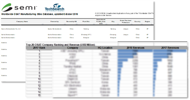

The Worldwide OSAT Manufacturing Sites Database reveals that while wire bond remains the largest volume interconnect by number of packages, the advanced packaging technologies such as bumping, wafer-level packaging, flip-chip assembly have seen tremendous growth. On the application side, mobile devices, HPC and 5G are expected to continue to drive innovation in the OSAT industry. The database also shows rising investment in advanced packaging and new test capabilities for 5G.

Combining the expertise of SEMI and TechSearch International, the Worldwide OSAT Manufacturing Sites Database update also features a section listing the revenues of the world’s top 20 OSAT companies in 2017 and 2018 and captures changes in technology capabilities and service offerings at various facilities.

OSAT Chart

The Worldwide OSAT Manufacturing Sites Database
is a comprehensive report offering insights into global OSAT facilities in China, Taiwan, Korea, Japan, Southeast Asia, Europe and the Americas. The report highlights new and emerging packaging offerings by manufacturing locations and companies. Specific details tracked include:

  • Plant site location, technology, and capability: Packaging, Test, and other product specializations, such as sensor, automotive and power devices are highlighted.
  • Packaging assembly service offered: BGA, specific leadframe type such as QFP, QFN, SO, flip-chip bumping, WLP, Modules/SIP, and sensors.
  • New manufacturing sites announced, planned or under construction.

Tracking advances in packaging technology – which directly affects chip performance, reliability and cost – requires understanding company offerings by location. Key features of the updated report include:

  • More than 120 companies and 360 facilities
  • More than 200 facilities with test capabilities
  • Over 90 facilities offering leadframe CSP
  • Over 50 bumping facilities, including 30 with 300mm wafer bumping capacity
  • More than 50 facilities offering WLCSP technology
  • New facilities offering FOWLP and FOPLP
  • More than 100 facilities in China, approximately 100 in Taiwan and 43 in Southeast Asia

The database findings are based on information gathered and compiled from over 120 companies globally. All information in the Worldwide OSAT Manufacturing Sites Database was gathered by SEMI and TechSearch International. Report licenses are available for single-user and multi-users. SEMI members save 16 percent or more depending on the type of license.

For more information about the Worldwide OSAT Manufacturing Sites Database and to order a sample copy, please click here. For pricing and ordering information, please click here.

About SEMI

SEMI® connects more than 2,100 member companies and 1.3 million professionals worldwide to advance the technology and business of electronics design and manufacturing. SEMI members are responsible for the innovations in materials, design, equipment, software, devices, and services that enable smarter, faster, more powerful, and more affordable electronic products. Electronic System Design Alliance (ESD Alliance), FlexTech, the Fab Owners Alliance (FOA) and the MEMS & Sensors Industry Group (MSIG) are SEMI Strategic Association Partners, defined communities within SEMI focused on specific technologies. Visit www.semi.org to learn more, contact one of our worldwide offices, and connect with SEMI on LinkedIn and Twitter.

About TechSearch International, Inc.
Founded in 1987, TechSearch International (Austin, Texas) is a technology licensing and consulting company specializing in accurate, relevant, and timely information on advanced packaging technology and market developments. Visit www.techsearchinc.com.

Association Contacts

Clark Tseng/SEMI
Phone: 886.3.560.1777 ext. 206
Email: [email protected]

Michael Hall/SEMI
Phone: 1.408.943.7988
Email: [email protected]

BRUSSELS, Belgium – November 19, 2019 – SEMI and 19 partners from 14 countries today launched an initiative to fill the skills gap and boost workforce diversity by tightening collaboration between the microelectronics industry and education providers. The project, dubbed METIS – Microelectronics Training, Industry and Skills – will focus on the skills and related training needed to support emerging verticals such as artificial intelligence (AI), autonomous driving and Industry 4.0.

semi-logo

A Sector Skills Alliance co-funded by the Erasmus+ Program, METIS is designed to overcome the skills shortage in the electronic components and systems value chain. Under METIS, SEMI and the partner organizations will establish a Microelectronics Observatory and Skills Council consisting of representatives from industry, academia, NGOs, think tanks and government. The consortium will develop a New Skills Strategy for the microelectronics industry in Europe with a focus on raising occupational profiles and skills critical to the future of the sector.

The project will boost online education and work-based learning in microelectronics design and manufacturing. METIS will also promote workforce diversity in the sector and target increased participation of under-represented groups in microelectronics education and employment. METIS, a four-year project, will receive 4 million EUR in public funding to be invested in microelectronics workforce development in Europe.

The talent shortage is one of the most severe issues challenging SEMI members today,” said Laith Altimime, president of SEMI Europe. “We are excited to partner with leading businesses and universities from across Europe to help build the robust talent pipeline crucial to microelectronics innovation and growth.”

MEITS Logo

“Digitalization is the key opportunity for the knowledge-oriented economy of our time, in particular for Europe, and semiconductor solutions are key drivers of digitalization,” said Dr. Sabine Herlitschka, CEO of Infineon Technologies Austria AG, a METIS consortium member. “Therefore, microelectronics offers highly attractive job opportunities at the forefront of research and applications relevant to all of us. With this project, we need to convey this enthusiasm for technology to more young talent, in particular women. One effective way of doing so is by tightening the collaboration between the industry and education institutions. This is a strategic core of our new METIS project.”  

Sector Skills Alliances work to improve skills intelligence and provide a clear strategy in a target sector through a double-barreled approach of identifying existing or emerging sector-specific labour market needs and enhancing the responsiveness of education and training organizations to industry needs. Sector Skills Alliances are established to facilitate cross-border certification and therefore ease professional mobility and increase recognition of qualifications at European level within a sector.

The METIS consortium consists of SEMI, Infineon, Bosch, X-FAB, Graphenea, Summa, Arcelik, Silicon Saxony, imec, Technical University of Graz, Dresden Chip Academy, University of South-Eastern Norway, Technical University of Sofia, Budapest University of Technology and Economics, IAL-FVG, Fast Track into Information Technology, European Association of Career Guidance, European Association for Women in Science, Engineering and Technology, CIMEA and DECISION.

About SEMI
SEMI® connects more than 2,100 member companies and 1.3 million professionals worldwide to advance the technology and business of electronics design and manufacturing. SEMI members are responsible for the innovations in materials, design, equipment, software, devices, and services that enable smarter, faster, more powerful, and more affordable electronic products. Electronic System Design Alliance (ESD Alliance), FlexTech, the Fab Owners Alliance (FOA) and the MEMS & Sensors Industry Group (MSIG) are SEMI Strategic Association Partners, defined communities within SEMI focused on specific technologies. Visit www.semi.org to learn more, contact one of our worldwide offices, and connect with SEMI on LinkedIn and Twitter.

Association and METIS Contact

Emir Demircan/SEMI Europe
Phone: +32 (0) 2 609 53 18
Email: [email protected]

MUNICH, Germany ─ November 12, 2019 ─ SEMICON Europa, Europe’s largest event connecting the entire electronics design and manufacturing supply chain – from innovation to applications – opens today in strategic co-location with productronica at Messe München, in Munich, Germany. Themed Semiconductors Drive Smart, SEMICON Europa 2019 – Nov. 12-15 – highlights the vital importance of European sectors and ecosystems in propelling the semiconductor manufacturing industry and the broader electronics design and manufacturing supply chain worldwide.

SEMICON Europa Logo

Olivier Schwab, Managing Director of the World Economic Forum, kicks off the Executive Keynote Opening Ceremony with his presentation Leadership in the Fourth Industrial Revolution. Thought leaders from the United Nations, Audi, IBM, Fraunhofer, Applied Materials and SOI Industry Consortium will present insights on sustainability, digital healthcare, smart automotive, IoT, quantum computing and other pressing topics surrounding the digital economy.

“The research and innovations arising from Europe are enabling substantial growth in the electronics sector and strengthening Europe's global position as a leading technology region, particularly in the automotive, medtech and MEMS markets,” said Laith Altimime, president of SEMI Europe. “With its global footprint, SEMI is well-positioned to leverage Europe’s core strengths in fostering regional collaboration to speed innovation and time-to-market for our members.”


SEMICON Europa Highlights
SEMICON Europa 2019 show floor programs highlight opportunities and challenges in smart segments such as medtech, manufacturing, design and workforce. The TechARENA features sessions on topics such as disruptive computing, communications technologies, photonics, MEMS, circular economy and 3D printing as the following forums and conferences provide insights into key segments.

Smart Mobility and Medtech Key Industry Growth Drivers
Smart mobility represents the largest opportunity for the semiconductor industry, with the automotive industry alone accounting for over 10 percent of all ICs produced globally. Carmakers and automotive suppliers in Europe are renowned for their focus on quality and innovation and have taken an active role in SEMI’s SMART Transportation initiative with their participation in its Global Automotive Advisory Council (GAAC). GAAC includes leading German companies such as Audi, Volkswagen, Bosch and Infineon. The SMART Transportation Forum spotlights the latest automotive trends and developments around autonomous driving, electrification and the push for zero defect.

Another thriving market for the semiconductor industry is medtech – where innovations promise to better the quality of human life and prolong the lives of people around the world. An epicenter for medtech innovation, Europe sets the pace for the rest of the world in digitizing healthcare. Leading startups, RTOs and multinationals driving innovation in digital health will present during the SMART MedTech Forum at the Inspiration Hub in Hall B2.

Focus on R&D and $2 Trillion Electronics Supply Chain
With research and development the heartbeat of new technology, representatives from leading European research institutes and R&D centers such as imec, CEA-Leti, Fraunhofer – all SEMI Strategic Association Partners – and VTT Technical Research Centre of Finland will present groundbreaking research and solutions at programs throughout SEMICON Europa. To help drive innovation across the $2 trillion electronics design and manufacturing supply chain, SEMICON Europa will feature SEMI  technology communities and partner associations including ESD Alliance, FlexTech, the Fab Owners Alliance and the MEMS & Sensors Industry Group.  

More SEMICON Europa Program Highlights

  • New for SEMICON Europa, the SMART Design session will highlight how advances in electronic system design are enabling emerging and future applications.
  • The SMART Workforce Forum will discuss how to keep the industry’s talent pipeline full and promote fair trade.
  • SEMI Industry Research & Statistics will present data to help SEMI members make informed business decisions. 
  • An array of Standards Meetings will focus on key technical issues in a year in which SEMI celebrates the publication of its 1000th standard.

For more details, please visit the SEMICON Europa website and connect with SEMI Europe on Twitter or LinkedIn @SEMIEurope (use #SEMICONEuropa).

About SEMI
SEMI® connects more than 2,100 member companies and 1.3 million professionals worldwide to advance the technology and business of electronics design and manufacturing. SEMI members are responsible for the innovations in materials, design, equipment, software, devices, and services that enable smarter, faster, more powerful, and more affordable electronic products. Electronic System Design Alliance (ESD Alliance), FlexTech, the Fab Owners Alliance (FOA) and the MEMS & Sensors Industry Group (MSIG) are SEMI Strategic Association Partners, defined communities within SEMI focused on specific technologies. Visit www.semi.org to learn more, contact one of our worldwide offices, and connect with SEMI on LinkedIn and Twitter.

Press Contact
Serena Brischetto, SEMI Europe
Email: [email protected]

MILPITAS, Calif. – November 12, 2019 – SEMI, the industry association serving the global electronics manufacturing and design supply chain, announced today that leading German vehicle manufacturer Volkswagen AG has joined SEMI. SEMI membership will give Volkswagen access to SEMI core competencies in developing international standards and harmonizing technology roadmaps while enabling the automaker to leverage the global SEMI platform to promote industry alignment across supply-chain segments.

semi-logo

Volkswagen is a founding member of the SEMI Global Automotive Advisory Council (GAAC). Anchoring the SEMI Smart Transportation vertical market platform, GAAC members address automotive technology issues such as device and system reliability and connectivity, promote industry standards, and align roadmaps of carmakers with adjacent industries to accelerate time to market. The GAAC has chapters in Europe, the U.S., Japan and Taiwan.

“Volkswagen has been a key catalyst in connecting the automotive and semiconductor value chains,” said Ajit Manocha, SEMI president and CEO. “Through its leadership in the SEMI Global Automotive Advisory Council and strong automotive stakeholder engagement, Volkswagen exemplifies SEMI’s mission to connect, collaborate and innovate as the GAAC works to accelerate advances in electric mobility and autonomous driving. We are excited to welcome Volkswagen to the SEMI family.”

Volkswagen Logo“The semiconductor industry is a role model for managing complexity, time-to-market and cost challenges and therefore holds the key to the automotive transformation,” said Dr. Rolf Zöller, Head of Electric/Electronics Development, Volkswagen AG. “With connected, secure and safe electronics the backbone of automated mobility and autonomous driving, aligning supply chain requirements and joint road mapping are mandatory for the future success of the automotive industry. On the strength of its global platform, SEMI is the association to enable close collaboration between the semiconductor and automotive industries.”

Under its leadership as a founding member of the GAAC, Volkswagen has been instrumental in establishing priorities for the Europe chapter and helped grow the chapter to encompass companies across the automotive electronics ecosystem including OEMs, device manufacturers, foundries, design companies, and equipment and materials suppliers.

Volkswagen, a member of the Volkswagen Group, is headquartered in Wolfsburg, Lower Saxony, Germany.

Smart Transportation is one of five SEMI vertical market platforms designed to bring together players in critical industry segments to advance innovation and help drive segment growth.

About Volkswagen

The Volkswagen Passenger Cars brand is present in more than 150 markets throughout the world and produces vehicles at over 50 locations in 14 countries. In 2018, Volkswagen delivered 6.2 million vehicles including bestselling models such as the Golf, Tiguan, Jetta or Passat. Currently, 195,878 people work for Volkswagen across the globe. The brand also has over 10,000 dealerships with 86,000 employees. Volkswagen is forging ahead consistently with the further development of automobile production. E-mobility, smart mobility and the digital transformation of the brand are the key strategic topics for the future.

About SEMI

SEMI® connects more than 2,100 member companies and 1.3 million professionals worldwide to advance the technology and business of electronics design and manufacturing. SEMI members are responsible for the innovations in materials, design, equipment, software, devices, and services that enable smarter, faster, more powerful, and more affordable electronic products. Electronic System Design Alliance (ESD Alliance), FlexTech, the Fab Owners Alliance (FOA) and the MEMS & Sensors Industry Group (MSIG) are SEMI Strategic Association Partners, defined communities within SEMI focused on specific technologies. Visit www.semi.org to learn more, contact one of our worldwide offices, and connect with SEMI on LinkedIn and Twitter.

SEMI Contact

Michael Hall
Phone: 1.408.943.7988
Email: [email protected]

Volkswagen AG Contact

Andreas Aal
Email: [email protected]

MILPITAS, Calif. — November 12, 2019 — Marking the fourth consecutive quarterly decline, worldwide silicon wafer area shipments totaled 2,932 million square inches in the third quarter of 2019, down 1.7 percent from the 2,983 million square inches shipped in the second quarter of the year and 9.9 percent lower than shipments during the same period in 2018, according to the SEMI Silicon Manufacturers Group (SMG) in its quarterly analysis of the silicon wafer industry.

semi-logo

"Global silicon wafer shipments continue to ship at lower volumes relative to last year’s record levels,” said Neil Weaver, chairman of SEMI SMG and vice president of Product Development and Applications Engineering at Shin Etsu Handotai America. “Ongoing geopolitical tensions and the overall economic slowdown have negatively impacted silicon demand for the year.”

Silicon Area Shipment Trends - Semiconductor Applications Only


Millions of Square Inches


1Q2018

2Q2018

3Q2018

4Q2018

1Q2019

2Q2019

3Q2019

Total

3,084

3,160

3,255

3,234

3,051

2,983

2,932

Source: SEMI (www.semi.org), November 2019

All data cited in this release includes polished silicon wafers, such as virgin test wafers and epitaxial silicon wafers, as well as non-polished silicon wafers shipped to end users. Silicon wafers are the fundamental building material for semiconductors, which are vital components of virtually all electronics goods, including computers, telecommunications products, and consumer electronics. The highly engineered thin, round disks are produced in various diameters – from one inch to 12 inches – and serve as the substrate material on which most semiconductor devices, or chips, are fabricated.

The SMG is a sub-committee of the SEMI Electronic Materials Group (EMG) and is open to SEMI members involved in manufacturing polycrystalline silicon, monocrystalline silicon or silicon wafers (e.g., as cut, polished, epi, etc.). The purpose of the SMG is to facilitate collective efforts on issues related to the silicon industry including the development of market information and statistics about the silicon industry and the semiconductor market.

More information on the SEMI Worldwide Silicon Wafer Shipment Statistics are available on the SEMI website.

About SEMI
SEMI® connects more than 2,100 member companies and 1.3 million professionals worldwide to advance the technology and business of electronics design and manufacturing. SEMI members are responsible for the innovations in materials, design, equipment, software, devices, and services that enable smarter, faster, more powerful, and more affordable electronic products. Electronic System Design Alliance (ESD Alliance), FlexTech, the Fab Owners Alliance (FOA) and the MEMS & Sensors Industry Group (MSIG) are SEMI Strategic Association Partners, defined communities within SEMI focused on specific technologies. Visit www.semi.org to learn more, contact one of our worldwide offices, and connect with SEMI on LinkedIn and Twitter.

Association Contact
Michael Hall, SEMI
Phone: 1.408.943.7988
Email: [email protected]

DRESDEN, Germany – 5 November, 2019 – Top experts in 3D integration and systems for semiconductor manufacturing will gather at the annual SEMI 3D & Systems Summit, 27-29 January, 2020, in Dresden, Germany, for the latest developments and insights in the 3D roadmap, heterogeneous integration and system-in-package technologies.3D in packaging and transistor cell design is critical to scaling the performance of integrated circuits to meet the demands of artificial intelligence (AI), machine learning and other data-intensive applications. Registration is now open with early-bird pricing until 30 November, 2019.

SEMI 3D & Systems Summit returns to Dresden for the second year with a broader scope of topics including:

3D Systems Summit Logo
  • 3DIC Through-Silicon-Via (TSV) technology
  • 2.5D, 3D FO-WLP/e-WLB
  • Heterogeneous Integration
  • Stacked dies and stacked wafers
  • 3D alternative technologies
  • 5G applications
  • uLED and photonics applications

Experts from Global Leaders to Present

Event speakers will explore disruptive applications such as mobile Internet of Things (IoT) and high-performance power electronics. 3D & Systems Summit presenters include experts from global leaders such as AMKOR, ASE Group, Dow, GLOBALFOUNDRIES, Savansys, SystemPlus, STMicroelectronics, TechSearch International, Yole Développement and Xperi.

The summit will showcase prominent players in 3D integration for microelectronics manufacturing while offering business-to-business matchmaking and networking for participants to explore new partnerships and other business opportunities. Visit 3D & Systems Summit for more information.

To reserve an exhibition space, contact Revi Gani at [email protected].

About SEMI

SEMI® connects more than 2,100 member companies and 1.3 million professionals worldwide to advance the technology and business of electronics design and manufacturing. SEMI members are responsible for the innovations in materials, design, equipment, software, devices, and services that enable smarter, faster, more powerful, and more affordable electronic products. Electronic System Design Alliance (ESD Alliance), FlexTech, the Fab Owners Alliance (FOA) and the MEMS & Sensors Industry Group (MSIG) are SEMI Strategic Association Partners, defined communities within SEMI focused on specific technologies. Visit www.semi.org to learn more, contact one of our worldwide offices, and connect with SEMI on LinkedIn and Twitter.

Association Contact

Serena Brischetto / SEMI Europe
Phone: +49 30 3030 8077-11
Email: [email protected]

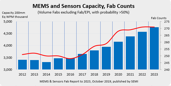
MILPITAS, Calif. — October 29, 2019 — Total worldwide installed capacity for MEMS and sensors fabs is forecast to grow 25 percent to 4.7 million wafers* per month from 2018 to 2023, driven by explosive demand across communications, transportation, medical, mobile, industrial and other Internet of Things (IoT) applications, according to the new MEMS & Sensors Fab Report to 2023 published by SEMI.

semi-logo

Listing more than 230 companies with over 400 facilities, the report is the first of its kind focused on MEMS and sensors front end facilities. The report, spanning the 12 years starting in 2012, predicts that MEMS fabs will account for 46 percent of all MEMS and sensors facilities by 2023. Image sensors fabs will represent 40 percent of the total, and other fabs – those producing both MEMS and image sensors – the remaining 14 percent.

Figure 1: Installed capacity and MEMS and sensors fab counts

Japan led the world in MEMS and sensors capacity in 2018, followed by Taiwan, the Americas, and Europe/Mideast. China is on track to rise from the sixth position this year to the third largest region in installed capacity by 2023. Japan and Taiwan are expected to maintain the top two positions through 2023.

The MEMS and Sensors Fab Report to 2023 shows fab equipment investments hovering at about US$4 billion per year from 2018 to 2023, with most of the spending – an estimated 70 percent – devoted to fabs for image sensors made on 300mm wafer sizes. During the same period, Japan’s fab equipment investment is expected to peak at nearly US$2 billion in 2020, with Taiwan topping out at US$1.6 billion in 2023.

All told, 14 new device volume fabs will be added from 2018 to 2023** for MEMS and sensors made on wafers ranging from 8 inches to 12 inches in size. China shows the largest increase in new volume fabs followed by Japan, Taiwan and Europe.

The MEMS & Sensors Fab Report to 2023 includes details on individual fabs such as location, technologies and products, as well as quarterly data from 2012 to 2023 for the following:

  • Construction and equipment investments
  • Installed capacities
  • Wafer sizes
  • Process nodes
MSIG Logo

SEMI Industry Research and Statistics developed the MEMS & Sensors Fab Report to 2023 in collaboration with the MEMS & Sensors Industry Group, a SEMI Strategic Association Partner. To learn more about the MEMS & Sensors Fab Report to 2023, click here.

*200mm equivalent capacity – excludes R&D, Pilot and EPI lines

**Excludes R&D, Pilot and EPI lines and fabs with low probabilities of being built
 

About SEMI

SEMI® connects more than 2,100 member companies and 1.3 million professionals worldwide to advance the technology and business of electronics design and manufacturing. SEMI members are responsible for the innovations in materials, design, equipment, software, devices, and services that enable smarter, faster, more powerful, and more affordable electronic products. Electronic System Design Alliance (ESD Alliance), FlexTech, the Fab Owners Alliance (FOA) and the MEMS & Sensors Industry Group (MSIG) are SEMI Strategic Association Partners, defined communities within SEMI focused on specific technologies. Visit www.semi.org to learn more, contact one of our worldwide offices, and connect with SEMI on LinkedIn and Twitter.

Association Contact

Michael Hall/SEMI
Phone: 1.408.943.7988
Email: [email protected]


MILPITAS, Calif. — October 22, 2019 — North America-based manufacturers of semiconductor equipment posted $1.95 billion in billings worldwide in September 2019 (three-month average basis), according to the September Equipment Market Data Subscription (EMDS) Billings Report published today by SEMI. The billings figure is 2.4 percent lower than the final August 2019 level of $2.00 billion, and is 6.0 percent lower than the September 2018 billings level of $2.08 billion.

“Monthly billings of North American equipment manufacturers declined for the second consecutive month,” said Ajit Manocha, president and CEO of SEMI. “However, year-over-year billings shows signs of bottoming, and recent capital expenditure increases for leading-edge logic will provide near-term billings growth opportunities."

The SEMI Billings report uses three-month moving averages of worldwide billings for North American-based semiconductor equipment manufacturers. Billings figures are in millions of U.S. dollars.


Billings
(3-mo. avg.)

Year-Over-Year

April 2019

$1,922.0

-28.5%

May 2019

$2,065.2

-23.6%

June 2019

$2.026.1

-18.4%

July 2019

$2,031.9

-14.6%

August 2019 (final)

$2,001.8

-10.5%

September 2019 (prelim)

$1,953.7

-6.0%

Source: SEMI (www.semi.org), October 2019

SEMI publishes a monthly North American Billings report and issues the Worldwide Semiconductor Equipment Market Statistics (WWSEMS) report in collaboration with the Semiconductor Equipment Association of Japan (SEAJ). The WWSEMS report currently reports billings by 24 equipment segments and by seven end market regions. SEMI also has a long history of tracking semiconductor industry fab investments in detail on a company-by-company and fab-by-fab basis in its World Fab Forecast and SEMI FabView databases. These powerful tools provide access to spending forecasts, capacity ramp, technology transitions, and other information for over 1,000 fabs worldwide. For an overview of available SEMI market data, please visit www.semi.org/en/MarketInfo.

The data contained in this release were compiled by David Powell, Inc., an independent financial services firm, without audit, from data submitted directly by the participants. SEMI and David Powell, Inc. assume no responsibility for the accuracy of the underlying data.

About SEMI

SEMI® connects more than 2,100 member companies and 1.3 million professionals worldwide to advance the technology and business of electronics design and manufacturing. SEMI members are responsible for the innovations in materials, design, equipment, software, devices, and services that enable smarter, faster, more powerful, and more affordable electronic products. Electronic System Design Alliance (ESD Alliance), FlexTech, the Fab Owners Alliance (FOA) and the MEMS & Sensors Industry Group (MSIG) are SEMI Strategic Association Partners, defined communities within SEMI focused on specific technologies. Visit www.semi.org to learn more, contact one of our worldwide offices, and connect with SEMI on LinkedIn and Twitter.

Association Contact

Michael Hall/SEMI
Phone: 1.408.943.7988
Email: [email protected]

Notes

Next SEMI Billings report is November 19, 2019 at 3:00pm Pacific.

For information on SEAJ Book-to-Bill Report, visit www.seaj.or.jp

TAIPEI, Taiwan – October 15, 2019 – Opening tomorrow, Energy Taiwan today hosts a pre-show press conference with photovoltaic (PV) and offshore wind power experts exploring the future of smart energy, industry trends, and strategies for seizing renewable energy business opportunities. The largest renewable energy event in Taiwan, Energy Taiwan connects the global green energy supply chain for three days of expert insights into the latest technologies and business opportunities in solar PV, offshore wind power, hydrogen energy, smart energy storage, and green finance and insurance.

Energy Taiwan Logo

Hosted by SEMI and the Taiwan External Trade Development Council (TAITRA), Energy Taiwan is expected to draw more than 12,000 visitors and 10,000 buyers from Taiwan and abroad to the Taipei Nangang Exhibition Center, Hall I, October 16-18, 2019.

Presenters at today’s press conference include:

Bringing together 165 exhibitors from 11 countries at more than 600 booths and experts across industry, government and academia, Energy Taiwan features three European pavilions – Germany, Denmark and the Netherlands – to encourage the exchange of renewable energy technologies and resources between Taiwan's domestic suppliers and international players.

To promote green energy government policy, SEMI and the Green Energy Industry Promotion Center will hold the Global Renewable Energy Supply Chain Summit. Green power industry experts and opinion leaders from the National Renewable Energy Certification Center, Taiwan Institute of Economic Research, Microsoft, and leading solar energy companies such as TSEC and Sinogreenergy will share insights on the future of green energy policies, market trends and application development strategies.

Energy Taiwan is held in conjunction with PV Taiwan, Wind Energy Taiwan, HFC Taiwan, and Smart Storage Taiwan during Renewable Energy Week, sponsored by the Bureau of Energy under the Ministry of Economics and SEMI. Renewable Energy Week highlights achievements of green energy policies implemented in 17 counties and cities in Taiwan.

Renewable Energy Week also gathers some of the most influential wind power developers in Taiwan including Swancor, Northland Power (NPI), Yushan Energy, Ørsted, Copenhagen Infrastructure Partners (CIP), wpd Taiwan Energy and Macquarie Capital to showcase their technical strengths in developing offshore wind power.

About SEMI
SEMI® connects more than 2,100 member companies and 1.3 million professionals worldwide to advance the technology and business of electronics design and manufacturing. SEMI members are responsible for the innovations in materials, design, equipment, software, devices, and services that enable smarter, faster, more powerful, and more affordable electronic products. Electronic System Design Alliance (ESD Alliance), FlexTech, the Fab Owners Alliance (FOA) and the MEMS & Sensors Industry Group (MSIG) are SEMI Strategic Association Partners, defined communities within SEMI focused on specific technologies. Visit www.semi.org to learn more, contact one of our worldwide offices, and connect with SEMI on LinkedIn and Twitter.

Association Contacts

Emmy Yi
E-mail: [email protected]
Tel: +886.3.560.1777 ext. 205

Eileen Lin
E-mail: [email protected]
Tel: +886.3.560.1777 ext. 288