downloadGroupGroupnoun_press release_995423_000000 copyGroupnoun_Feed_96767_000000Group 19noun_pictures_1817522_000000Member company iconResource item iconStore item iconGroup 19Group 19noun_Photo_2085192_000000 Copynoun_presentation_2096081_000000Group 19Group Copy 7noun_webinar_692730_000000Path
Skip to main content
Default Banner Image

SEMI Press Release

ID
semi-press-release

GRENOBLE, France – 30 July, 2019 – More than 400 electronics industry experts will gather at SEMI MEMS & Imaging Sensors Summit, 25-27 September, 2019 in Grenoble, France, for the latest MEMS and imaging sensors developments and innovations that are advancing the user experience with hundreds of millions of smart devices. MEMS and imaging sensors power a wide range of applications including autonomous systems for transportation and agriculture, cellular security systems, mixed reality (MR) headsets and biomedical wearables.  Registration is open now with early-bird pricing available until August 17, 2019.
MEMS & Imaging Sensors Summit Logo

The SEMI MEMS & Imaging Sensors Summit will also showcase how companies now combine intelligent sensing with data analytics, low-power networks, and machine learning for smart city applications such as smart parking, smart irrigation, smart construction and smart lighting.

Featuring both MEMS technology and Imaging sensors tracks, the Summit opens with executive keynotes by Alibaba, TowerJazz, Microsoft, and VTT and addresses by Claudia Levo, executive vice president, Integrated Marketing and Communications, STMicroelectronics, and Laith Altimime, president, SEMI Europe.

“Exciting advancements in MEMS and imaging sensors are changing the way we live, work and play,” said Laith Altimime, president, SEMI Europe. “With MEMS and imaging sensors so synergistic, this year we offer a unified conference with industry leaders across multiple markets providing insights on cutting-edge trends and technical innovations, all under one roof. Global experts will network and collaborate across the supply chain and market segments – from transportation and industrial to consumer mobile and biomedical – to drive the development of next-generation smart devices.”

Executive Keynote Presentations

  • Sean Ding, Chief Scientist of AIoT, Alibaba Cloud Intelligent, Digitize the Physical World — Ding will discuss how Alibaba Cloud’s Internet of Things (IoT) platform is accelerating the rollout of sensors across a broad range of applications.
  • Avi Strum, Senior Vice President and General Manager of Sensor Business Group, TowerJazz, Considerations of Optical Fingerprint and 3D Face Recognition Sensors for Cellular Security Applications — Strum will discuss the evolution of security features in the cellular market and the role of sensors.
  • Sunil Acharya, Senior Director of Sensor Development HoloLens, Microsoft, Sensors in Mixed Reality — Acharya will explore holographic mixed reality and explain the innovative algorithms and sensors it developed for Microsoft HoloLens 2.
  • Antti Vasara, President and CEO at VTT, A Touch of Finnish Sense — Vasara will discuss how sensor fusion, artificial intelligence (AI) and other innovations enable new solutions to global challenges.

Other SEMI MEMS & Imaging Sensors Summit Highlights

  • New – Download the event app to participate in B2B Matchmaking
  • Technology Showcase – See companies stage live demonstrations of products powered by MEMS and imaging sensor devices as they compete for audience votes.
  • The Exhibition Area – Meet innovators driving the future of MEMS and imaging sensors design and manufacturing.
  • Attend networking events such as the welcome reception and gala dinner held for all summit attendees and exhibitors.

The Summit will be at the WTC in Grenoble, France.

Stay in touch on Twitter @SEMIEurope: #SensorsSummit #MEMS #Imaging #IoT #AI #SEMIEurope

Premier Sponsors

For more information including the full event agenda, please visit the SEMI MEMS & Imaging Sensors Summit website.

About SEMI

SEMI® connects more than 2,100 member companies and 1.3 million professionals worldwide to advance the technology and business of electronics design and manufacturing. SEMI members are responsible for the innovations in materials, design, equipment, software, devices, and services that enable smarter, faster, more powerful, and more affordable electronic products. Electronic System Design Alliance (ESD Alliance), FlexTech, the Fab Owners Alliance (FOA) and the MEMS & Sensors Industry Group (MSIG) are SEMI Strategic Association Partners, defined communities within SEMI focused on specific technologies. Visit www.semi.org to learn more, contact one of our worldwide offices, and connect with SEMI on LinkedIn and Twitter.

Press Contact

Serena Brischetto/SEMI Europe
Email: [email protected]
 

MILPITAS, Calif. — July 23, 2019 — Worldwide silicon wafer area shipments totaled 2,983 million square inches in the second quarter of 2019, down 2.2 percent from the 3,051 million square inches shipped in the first quarter of the year and 5.6 percent lower than shipments during the same period in 2018, according to the SEMI Silicon Manufacturers Group (SMG) in its quarterly analysis of the silicon wafer industry. 

"Global silicon wafer shipment are being impacted by the same headwinds that are facing the broader industry,” said Neil Weaver, chairman SEMI SMG and vice president, Product Development and Applications Engineering of Shin Etsu Handotai America. “While shipment area growth is currently subdued, the long-term outlook for the industry remains positive.”


Silicon Area Shipment Trends - Semiconductor applications only


Millions of Square Inches


4Q2017

1Q2018

2Q2018

3Q2018

4Q2018

1Q2019

2Q2019

Total

2,977

3,084

3,160

3,255

3,234

3,051

2,983


Source: SEMI (www.semi.org), Jul 2019


All data cited in this release includes polished silicon wafers, such as virgin test wafers and epitaxial silicon wafers, as well as non-polished silicon wafers shipped to end users.

Silicon wafers are the fundamental building material for semiconductors, which, in turn, are vital components of virtually all electronics goods, including computers, telecommunications products, and consumer electronics. The highly engineered thin, round disks are produced in various diameters – from one inch to 12 inches – and serve as the substrate material on which most semiconductor devices, or chips, are fabricated.

The SMG is a sub-committee of the SEMI Electronic Materials Group (EMG) and is open to SEMI members involved in manufacturing polycrystalline silicon, monocrystalline silicon or silicon wafers (e.g., as cut, polished, epi, etc.). The purpose of the SMG is to facilitate collective efforts on issues related to the silicon industry including the development of market information and statistics about the silicon industry and the semiconductor market.

More information on the SEMI Worldwide Silicon Wafer Shipment Statistics are available on the SEMI website.

About SEMI
SEMI® connects more than 2,100 member companies and 1.3 million professionals worldwide to advance the technology and business of electronics design and manufacturing. SEMI members are responsible for the innovations in materials, design, equipment, software, devices, and services that enable smarter, faster, more powerful, and more affordable electronic products. Electronic System Design Alliance (ESD Alliance), FlexTech, the Fab Owners Alliance (FOA) and the MEMS & Sensors Industry Group (MSIG) are SEMI Strategic Association Partners, defined communities within SEMI focused on specific technologies. Visit www.semi.org to learn more, contact one of our worldwide offices, and connect with SEMI on LinkedIn and Twitter.

Association Contact
Michael Hall, SEMI
Phone: 1.408.943.7988
Email: [email protected]

MUNICH, Germany ─ July 23, 2019 ─ SEMICON Europa, Europe’s largest event connecting the entire electronics design and manufacturing supply chain, from innovation to application, will spotlight smart technologies and the talent vital to continuing industry growth 12-15 November, 2019 at Messe München, in Munich, Germany. Registration is open for visitors and exhibitors.

Co-located with productronica, SEMICON Europa will highlight challenges and opportunities in Smart segments such as automotive, medtech, manufacturing and fab management including MEMS and sensors. Europe’s research and development hubs, chipmakers, and materials and equipment companies are strategically positioned in the global electronics value chain to shape the development and growth of Smart applications.

SEMICON Europa Logo

“Collaboration and investments in key Smart application segments including medtech and automotive where Europe plays a central role are crucial to continuing innovation by the European semiconductor industry,” said Laith Altimime, president of SEMI Europe. “SEMICON Europa is the premier platform in Europe for gathering key players across the value chain for the collaboration critical to exploiting opportunities in Smart application development.”

To strengthen Europe´s strategic leadership and inspire the development of new products and technologies, SEMI this year formed partnerships with imec, CEA-Leti and Fraunhofer, three of the world’s top technology research and innovation centers. Europe received additional support from Bosch, Infineon and Intel Ireland. For the first time in decades, all three European chipmakers invested heavily in new 300mm wafer fabs to help fuel the digital economy.

Also earlier this year, German luxury automobile maker Audi AG became the first automotive original equipment manufacturer (OEM) to join SEMI as member, strengthening alignment across automotive supply-chain segments. At SEMICON Europa, the SMART Transportation Forum and Pavilion, led by the SEMI Global Automotive Advisory Council (GAAC) and bolstered by SEMI Strategic Association Partner ESD (Electronic System Design), will gather key stakeholders across the automotive value chain, from design and semiconductor equipment to materials and carmaking, to explore innovation opportunities in automotive electronics.

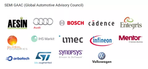
SEMI GAAC (Global Automotive Advisory Council)

SEMI GAAC (Global Automotive Advisory Council)

SEMICON Europa highlights include:


Inspiration Hub

The all-new Inspiration Hub at SEMICON Europa will feature SMART Workforce and SMART MedTech programs. The new SMART MedTech program will showcase how semiconductors are enabling technology innovation and solutions to global healthcare challenges.

The Inspiration Hub will give special focus to workforce development as innovators, entrepreneurs, students, engineers and key stakeholders in the European semiconductor and medtech ecosystems meet to discuss career opportunities. The Innovation Hub’s SMART Workforce program takes aim at helping the electronics industry overcome its critical workforce shortage and build the talent pipeline. Students will also learn how technology innovation is solving global challenges in the semiconductor industry.

Complementing the SEMICON Europa SMART Workforce program, the Accelerating Talents program in collaboration with productronica and VDMA will connect international corporations and start-ups looking for young talent.

Smart Technology

The TechARENA will highlight the latest trends and innovations in key areas such as Smart design, disruptive computing, 3D printing, photonics, MEMS, 5G and environment, health and safety (EHS).

SEMICON Europa Premier Sponsors

Silver sponsor: KLA

Event sponsors: Atotech, DAS Environmental Expert, Ebara, Edwards, EV Group, Inficon, JSR Micro, Lam Research, Pfeiffer Vacuum, Rena Technologies, Screen, Siconnex Customized Solutions, Tokyo Electron.

For more details, please visit the SEMICON Europa website and connect with SEMI Europe on Twitter or LinkedIn @SEMIEurope (use #SEMICONEuropa).

About SEMI

SEMI® connects more than 2,100 member companies and 1.3 million professionals worldwide to advance the technology and business of electronics design and manufacturing. SEMI members are responsible for the innovations in materials, design, equipment, software, devices, and services that enable smarter, faster, more powerful, and more affordable electronic products. Electronic System Design Alliance (ESD Alliance), FlexTech, the Fab Owners Alliance (FOA) and the MEMS & Sensors Industry Group (MSIG) are SEMI Strategic Association Partners, defined communities within SEMI focused on specific technologies. Visit www.semi.org to learn more, contact one of our worldwide offices, and connect with SEMI on LinkedIn and Twitter.


Press Contact

Serena Brischetto, SEMI Europe
Email:
[email protected]

 

MILPITAS, Calif. – July 15, 2019 – SEMI, the global industry association representing the electronics design and manufacturing supply chain, today announced a memorandum of understanding (MOU) with FIRST Global, a non-profit that organizes the FIRST Global Challenge, an annual international robotics event dedicated to inspiring a passion for STEM (Science, Technology, Engineering and Math) among young students worldwide. Under the agreement, SEMI will leverage its global platform to help bring the FIRST Global Challenge to more young students around the world and inspire them to pursue a STEM education.

semi-logo

The MOU aligns with SEMI Works, the holistic SEMI program designed to improve the industry's image and provide  programs for all age groups across the education continuum. SEMI Works aims to strengthen the semiconductor industry’s talent pipeline and overcome its shortage of skilled workers.

“With workforce development a top strategic priority at SEMI, supporting FIRST Global makes sense as it gives young people around the world opportunities to collaborate and helps expose them to STEM careers through experiential learning opportunities,” said Ajit Manocha, SEMI president and CEO. “We are excited to be partnering with FIRST Global, which shares SEMI’s passion for inspiring young students to pursue educations and ultimately careers in STEM disciplines.”

Dean Kamen, the legendary inventor of the Segway and a tireless advocate for science and technology, established FIRST Global. The inaugural 2017 FIRST Global Challenge included teams from more than 150 countries. In his keynote last week at SEMICON West, Kamen discussed how the industry can develop the next generation of talent critical to innovation as well as the FIRST Global Challenge.

About FIRST Global

FIRST® Global was established as a US-based 501(c)(3) not-for-profit public charity to provide the framework for an “Olympics”-style robotics challenge, inviting one team from every nation to participate in an international robotics event that builds bridges between high school students with different backgrounds, languages, religions, and customs. By bringing these future STEM leaders together in an engaging and collaborative competition that drives home the importance, excitement, and applicability of STEM education, FIRST Global inspires students to learn the skills they will need to make the discoveries their parents and grandparents would consider miracles, impossibilities, or just plain science fiction. FIRST Global also strives to convince the various national governments and organizations of the world to embrace STEM education, and to support it by investing in their young adults that will soon begin to make their marks in the world. Visit https://first.global/ to learn more and to get involved!


About SEMI

SEMI® connects more than 2,100 member companies and 1.3 million professionals worldwide to advance the technology and business of electronics design and manufacturing. SEMI members are responsible for the innovations in materials, design, equipment, software, devices, and services that enable smarter, faster, more powerful, and more affordable electronic products. Electronic System Design Alliance (ESD Alliance), FlexTech, the Fab Owners Alliance (FOA) and the MEMS & Sensors Industry Group (MSIG) are SEMI Strategic Association Partners, defined communities within SEMI focused on specific technologies. Visit www.semi.org to learn more, contact one of our worldwide offices, and connect with SEMI on LinkedIn and Twitter.


Association Contact
Michael Hall/SEMI
Phone: 1.408.943.7988
Email: [email protected]


SAN FRANCISCO, Calif. — July 10, 2019 — SEMI yesterday honored five industry leaders at SEMICON West 2019 for their outstanding accomplishments in developing Standards for the electronics and related industries. The SEMI Standards awards were announced at the SEMI International Standards 1000th Standard Celebration.

SEMICON West Logo

SEMI Standards Excellence Award Inspired By Karel Urbanek

The SEMI Standards Excellence award is the most prestigious honor for participants in the SEMI International Standards program. The award is inspired by the leadership of Karel Urbanek, who led the program with dignity, diplomacy, fairness, honesty, and enthusiasm through the difficult early years of internationalization. The award has been presented since 1992 to outstanding program members epitomizing Mr. Urbanek’s fine qualities and dedication.

This year the Excellence Award is presented to Dr. James Moyne of Applied Materials and the University of Michigan.

As Standards and Technology Specialist for the Applied Materials Global Services Group, Dr. Moyne has been an active developer of advanced process control in the area of predictive feedback and a frequent presenter at ASMC. He received the 2015 ASMC best paper award for his discussion on the emergence of big data in the semiconductor industry.

As an Associate Research Scientist at the University of Michigan, he researches advanced process control technologies and systems as well as smart manufacturing concepts such as digital twin and predictive solutions.

His many efforts have provided the foundation for realizing smart manufacturing concepts in the microelectronics industries. He has made a major contribution by leading the development of standards that have enabled improvements in the quality and efficiency of high-volume semiconductor manufacturing.

Dr. Moyne is co-author of SEMI standards in the areas of process control (including E133 and E126), sensor bus (E54), and big data (E148 and E160). These standards are the basis for run-to-run control and fault detection and classification, key elements of advanced process control, where the microelectronics industry excels over other industries.

He has been a tireless supporter of advanced process control in SEMI Standards, and other microelectronics-related associations, chairing the IMA-APC Council and the International Roadmap for Devices and Systems (IRDS) Factory Integration focus group. He has also co-chaired the annual APC Conference in the United States for the past seven years. In addition, he is active in the SEMI Smart Manufacturing Technology Community and continuously looks for opportunities to introduce relevant SEMI Standards to the world outside of SEMI.

Dr. Moyne is currently a co-chair of the North America Information and Control Committee and leads the Sensor Bus Task Force and Process Control System Task Force. Most recently. He played a critical role in the formation of task forces in both Taiwan and North America that are taking on fab equipment and data security issues.


Standards Awards - James Moyne

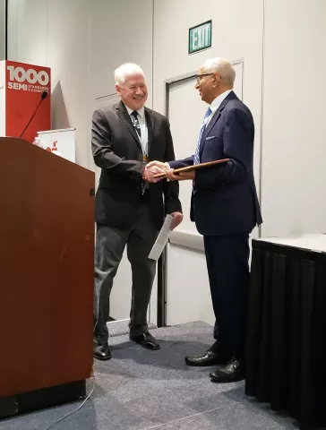
Dr. James Moyne (Applied Materials/University of Michigan) and Ajit Manocha (SEMI, CEO)
 

Standards2019

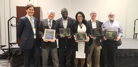
From Left to Right: James Amano (SEMI), Dr. James Moyne (Applied Materials/University of Michigan), Yaw Obeng (NIST) received the award for Richard Allen (NIST), Cristina Chu (ASM-NEXX), Michael O’Brien (Intel) received the award for Stefan Radloff (Intel), Eric Sklar (Safety Guru)


Merit Award

Eric Sklar (Safety Guru) leads the Energetic Materials Task Force and has led the improbable task of shepherding SEMI Document 5761, Safety Guideline for Use of Energetic Materials in Semiconductor R&D and Manufacturing Processes to publication as SEMI S30-0719.

Over 70 incidents have been reported related to the use of new energetic compounds, causing loss of life, significant facility damage, and production interruption. The fallout spurred several leading semiconductor device manufacturers, including GLOBALFOUNDRIES, IBM, Intel, Samsung, SK Hynix, TI, and TSMC, to identify the need for a comprehensive, international, best-known-methods safety guideline for equipment and practices for process chemicals and byproducts that have or may exhibit energetic properties.

As many stakeholders are involved, deriving the best industry practices and safety guidelines that satisfy chemical suppliers, equipment manufacturers, consultants, third party evaluators, and others involved in the semiconductor field was extremely difficult.

The ballot was initially issued in 2015 but failed multiple times due to significant disagreement. Eric Sklar agreed to take up the activity as new task force leader, and the document went through additional revisions in 2017 and 2018, getting closer to industry consensus but ultimately failing with each re-ballot. In April 2019, on the sixth try, Document 5761 was approved by the EHS Technical Committee. Sklar took on a very complex problem at the task force level, won industry support, and drove the project to completion.

Sklar has been a SEMI Standards volunteer for more than three decades. Currently, he co-leads the SEMI S3 (Liquid Heating System) Revision, Fire Protection, and S10 (Risk Assessment) Revision task forces.

Leadership Award

Three members were recognized with the SEMI Standards Leadership Award for the publication of a significant back-end standard, SEMI 3D20-0619, Specification for Panel Characteristics for Panel Level Packaging (PLP) Applications.

While the precedent for wafer dimension standards was set long ago, this standard represents the first time the industry has standardized a panel size. The standard will help accelerate the adoption of PLP by eliminating the need to customize equipment and materials for a variety of panel sizes.

Cristina Chu (ASM-NEXX) spearheaded the formation of the Panel Level Packaging (PLP) Panel Task Force at the Fall 2017 Meetings. The task force is chartered to develop standards for panels used in panel level processing. Cristina overcame the challenge of balancing the various interests of multiple groups by building a consensus through extensive teleconferencing, often twice a day, to accommodate members throughout the world. Through her leadership and diplomacy skills, Cristina strengthened collaboration of stakeholders across the supply chain and within the international community.

Richard Allen (NIST) co-led the Panel Level Packaging (PLP) Panel Task Force. Rich’s extensive experience in the SEMI Standards Program was critical in determining the parameters to include in the ballot. Rich continues to be a key force in pushing topics through the SEMI Standards process. In addition to co-leading the task force, he has also chaired the 3D Packaging and Integration Technical Committee since 2011 and helped drive results on other task forces.

Stefan Radloff (Intel), a longtime SEMI Standards Program member, attended his first meeting in spring 1996. Radloff brought the voice of the customer to the effort to ensure end-user adoption of the task force’s proposals. After learning of SEMI activity around standardizing panel dimensions, Stefan joined the task force and was instrumental in driving the activity to completion. Stefan also served as the Physical Interfaces and Carriers North American Technical Committee Co-chair for several years and was previously involved in the development of the 300 mm physical interface standards, next generation reticle carrier standards, and 450 mm standards.

About SEMI

SEMI® connects more than 2,100 member companies and 1.3 million professionals worldwide to advance the technology and business of electronics design and manufacturing. SEMI members are responsible for the innovations in materials, design, equipment, software, devices, and services that enable smarter, faster, more powerful, and more affordable electronic products. Electronic System Design Alliance (ESD Alliance), FlexTech, the Fab Owners Alliance (FOA) and the MEMS & Sensors Industry Group (MSIG) are SEMI Strategic Association Partners, defined communities within SEMI focused on specific technologies. Visit www.semi.org to learn more, contact one of our worldwide offices, and connect with SEMI on LinkedIn and Twitter.

Association Contact
Michael Hall, SEMI
Phone: 1.408.943.7988
Email: [email protected]

SEMI Announces Election and Re-Election of Board Members

SAN FRANCISCO, Calif. — July 10, 2019 — SEMI today announced at SEMICON West 2019 the election of Kazuo Ushida, Chairman of the Board, Representative Director, Nikon Corporation, as a new member of the SEMI International Board. In addition, SEMI confirmed the re-election of six current members to the SEMI International Board of Directors in accordance with the association's by-laws.

semi-logo

The following six Board members were re-elected for two-year terms:

  • Michael Allison, CEO, VAT
  • Bertrand Loy, president and CEO, Entegris
  • Daisuke Murata, president and CEO, Murata Machinery
  • Stephen Schwartz, president and CEO, Brooks Automation
  • Kyu Dong (KD) Sung, CEO, EO Technics
  • Xinchao Wang, Honorary Chairman, JCET

The SEMI Executive Committee confirmed Bertrand Loy, president and CEO of Entegris, as chairman of the SEMI Executive Committee. SEMI also confirmed Kevin Crofton, president of SPTS and corporate vice president at Orbotech, as vice-chairman. 

The leadership appointments and the elected board members’ tenure become effective at the annual SEMI membership meeting on July 10, during SEMICON West 2019 in San Francisco, California.  

“The SEMI Board of Directors is comprised of global business leaders who represent SEMI members and the industry, ensuring that SEMI develops and delivers member value in all regions,” said SEMI president and CEO Ajit Manocha. “We congratulate the newly elected and re-elected members and greatly appreciate all of our board members’ contributions to the industry.”

SEMI’s 17 voting directors and 11 emeritus directors represent companies from Europe, China, Japan, Korea, North America, and Taiwan, reflecting the global scope of the association’s activities. SEMI directors are elected by the general membership as voting members of the board and can serve a total of five two-year terms.

About SEMI

SEMI® connects more than 2,100 member companies and 1.3 million professionals worldwide to advance the technology and business of electronics design and manufacturing. SEMI members are responsible for the innovations in materials, design, equipment, software, devices, and services that enable smarter, faster, more powerful, and more affordable electronic products. Electronic System Design Alliance (ESD Alliance), FlexTech, the Fab Owners Alliance (FOA) and the MEMS & Sensors Industry Group (MSIG) are SEMI Strategic Association Partners, defined communities within SEMI focused on specific technologies. Visit www.semi.org to learn more, contact one of our worldwide offices, and connect with SEMI on LinkedIn and Twitter.

Association Contact

Michael Hall
SEMI
Email: [email protected]
Phone: 1.408.943.7988

CyberOptics MRS Sensor Wins 2019 Best of West Award – Delivers Ultra-High Quality 3D Images and High-Speed Inspection

SAN FRANCISCO, Calif. — July 10, 2019 — SEMI, the global industry association representing the electronics manufacturing and design supply chain, and Semiconductor Digest today announced that the CyberOptics NanoResolution MRS Sensor has won the 2019 Best of West award at SEMICON West, the flagship event for the U.S. semiconductor industry. The award recognizes important product and technology developments in the electronics manufacturing supply chain. Best of West finalists were selected based on their financial impact on the industry, engineering or scientific achievement, and/or societal impact.

semicon-west-beyond-smart

The proprietary MRS sensor technology, deemed best-in-class, enables metrology-grade accuracy by inhibiting optical measurement distortions and reflections. CyberOptics’ unique sensor architecture simultaneously captures and transmits multiple images in parallel while proprietary 3D fusing algorithms merge the images. The result is ultra-high quality 3D images and high-speed inspection.

“There’s a big emphasis on metrology at this year’s SEMICON West,” said Pete Singer, editor in chief of Semiconductor Digest. “The CyberOptics MRS Sensor is a great example of a fantastic new tool now available to semiconductor manufacturers.”

The Best of West award will be presented today at SEMICON West.

Platinum Sponsors for SEMICON West are Applied Materials, KLA, Lam Research and TEL, Other top sponsors include AEM Singapore, ASE, Burr & Forman LLP, Edwards, eSilicon Corporation, SAP and Silvaco.

More information is available on the SEMICON West 2019 website.

Follow SEMICON West and the AI Design Forum on Twitter: @SEMIconex – #SEMICONWest, #AIDesignForum

About Semiconductor Digest

Through a mix of news, contributed articles and staff-written articles, Semiconductor Digest is dedicated to providing global information about the design, manufacturing, packaging and testing of semiconductors and other types of electronic devices, including MEMs, LEDs, displays, power electronics, optoelectronics/photonics, biomedical devices, solar cells, thin film batteries and flexible electronics. Semiconductor Digest consists of a website, magazine and topic-focused newsletters.

About SEMI

SEMI® connects more than 2,100 member companies and 1.3 million professionals worldwide to advance the technology and business of electronics design and manufacturing. SEMI members are responsible for the innovations in materials, design, equipment, software, devices, and services that enable smarter, faster, more powerful, and more affordable electronic products. Electronic System Design Alliance (ESD Alliance), FlexTech, the Fab Owners Alliance (FOA) and the MEMS & Sensors Industry Group (MSIG) are SEMI Strategic Association Partners, defined communities within SEMI focused on specific technologies. Visitwww.semi.org to learn more, contact one of our worldwide offices, and connect with SEMI on LinkedIn and Twitter.


Association Contacts

Michael Hall/SEMI
Phone: 1.408.943.7988
Email: [email protected]

Scott Stevens, Cardinal Communications for SEMI Americas
Phone: 1.512.288.4050
Email: [email protected]


Semiconductor Digest Contact

Pete Singer, Editor in Chief
Phone: 1.978.470.1806
Email: [email protected]

SEMICON West 2019 Opens with Smart Technologies, Workforce Development, Industry Opportunities in Spotlight

SAN FRANCISCO, Calif. — July 9, 2019 — Smart technologies take center stage today as SEMICON West, the flagship U.S. event for connecting the electronics manufacturing and design supply chain, opens for three days of insights into leading technologies and applications that will power future industry expansion. July 9-11, 2019, at the Moscone Center in San Francisco, SEMICON West 2019 spotlights how cognitive learning technologies and other disruptors will transform industries and lives. Register online and on site.

semicon-west-beyond-smart

Themed BEYOND SMART and presented by SEMI, SEMICON West 2019 features top technologists and industry leaders highlighting cutting-edge technologies such as artificial intelligence (AI), Internet of Things (IoT) and quantum computing and trends in Smart Transportation, Smart Manufacturing, Smart Medtech, Smart Data and workforce development.  

Eight keynotes and more than 250 subject matter experts will offer insights into critical opportunities and issues across the global microelectronics supply chain. The event also features Smart Pavilions to showcase interactive technologies for immersive, virtual experiences.

SEMICON West 2019 opening day features keynotes and executive panels at the nearby Blue Shield of California Theater in the Yerba Buena Center for the Arts.

SEMICON West 2019 highlights include:

  • Legendary inventor Dean Kamen, called “the next Thomas Edison” by Forbes magazine, joins top executives from Advanced Micro Devices, Applied Materials, IBM, Synopsis and W20 Group on opening day to present at the AI Design Forum: The Future of Computing – from Materials to Systems.
  • The Quantum Advantage in advancing applications for sensing and communications comes into sharp focus as IBM showcases its IBM Q quantum computer model on the SEMICON West show floor. IBM Q is the industry’s first initiative to build universal quantum computers for business and science. Industries expected to benefit soon from quantum computing include automotive, medical, financial and energy. The exhibit features demonstrations of the IBM Q Experience quantum cloud services platform and Qiskit, an open source quantum software framework.
  • The Quantum Economic Development Consortium (QED-C), established in late 2018 by companies including Boeing and IBM and the U.S Department of Commerce’s National Institute of Standards and Technology (NIST), presents a progress update.  
  • Theme pavilions provide insights into the latest developments and trends in Smart Design, Smart Manufacturing, Smart Medtech, Smart Workforce, and Smart Transportation including leading-edge electric cars.
  • The 2019 SEMI Americas Award recognizes technology developments with a major impact on the semiconductor industry and the world.
  • The 2019 Best of West Award celebrates innovative new products or services that are significantly advancing the electronics manufacturing supply chain or a manufacturing capability.

Visit the SEMICON West 2019 website for the complete list of keynotes and executive panels and the full agenda of speakers and panel discussions. ES Design West, presented by SEMI Strategic Association Partner Electronic System Design Alliance, is co-located with SEMICON West 2019.

Platinum Sponsors for SEMICON West are Applied Materials, KLA, Lam Research and TEL. Other top sponsors include AEM Singapore, ASE, Burr & Forman LLP, Edwards, eSilicon Corporation, SAP and Silvaco.

SEMICON West is the culmination of eight progressive conferences that comprise SEMI’s inaugural Technology Leadership Series of the Americas. More information is available on the SEMICON West 2019 website.

Follow SEMICON West and the AI Design Forum on Twitter: @SEMIconex, #SEMICONWest, #AIDesignForum

About SEMI

SEMI® connects more than 2,100 member companies and 1.3 million professionals worldwide to advance the technology and business of electronics design and manufacturing. SEMI members are responsible for the innovations in materials, design, equipment, software, devices, and services that enable smarter, faster, more powerful, and more affordable electronic products. Electronic System Design Alliance (ESD Alliance), FlexTech, the Fab Owners Alliance (FOA) and the MEMS & Sensors Industry Group (MSIG) are SEMI Strategic Association Partners, defined communities within SEMI focused on specific technologies. Visit www.semi.org to learn more, contact one of our worldwide offices, and connect with SEMI on LinkedIn and Twitter.

Association Contacts

Michael Hall/SEMI
Phone: 1.408.943.7988
Email: [email protected]

Scott Stevens, Cardinal Communications for SEMI Americas
Phone: 1.512.288.4050
Email: [email protected]


1,000th SEMI Industry Standard Marks 40+ Years of Microelectronics Innovation

SEMI reaches milestone with publication of energetic materials safety guideline

SAN FRANCISCO ─ July 9, 2019 ─ SEMI, the global industry association representing the electronics manufacturing and design supply chain, announced today at SEMICON West the publication of the 1,000th SEMI international Standard since the launch of the program in 1973. A linchpin of innovation for electronics manufacturing, SEMI Standards make possible smaller, faster and smarter electronics that have transformed the way we live and work.

semi-logo

“SEMI Standards are the oxygen of the electronics industry, speeding product development, boosting product reliability, driving down manufacturing costs, and increasing factory efficiency while improving worker safety,” said Ajit Manocha, SEMI president and CEO. “Electronics have evolved to deliver greater social good across automotive, healthcare, agriculture and countless other industries that touch our daily lives. These innovations all start with SEMI Standards.”

SEMI Standards are as pervasive as their impact is profound. They have enabled the production of more than 2.2 billion wafers, 1.8 trillion IC devices. A purchase order for a piece of semiconductor processing equipment typically cites an average of 25 SEMI Standards. The 1,000 SEMI Standards include protocols for hardware and software communication, traceability, 3D-IC, compound semiconductors, facilities, MEMS, metrics, silicon wafer, carriers and automation systems. The Standards are used in many segments including display, photovoltaic, printed circuit board manufacturing and high-brightness LEDs.

1000 Standards Logo

The 1,000th SEMI Standard – SEMI S30 – defines the safe use and handling of energetic materials, the potentially hazardous process chemicals used increasingly in semiconductor manufacturing to spur advances in materials purity, integrity and quality. SEMI S30 is titled EHS Guideline for Use of Energetic Materials in Semiconductor R&D and Manufacturing Processes.

“SEMI S30 exemplifies the tremendous value of standards to the electronics manufacturing supply chain,” said James Amano, senior director of International Standards and EHS at SEMI. “Chemical suppliers, equipment manufacturers, semiconductor manufacturers and third-party evaluators can now follow SEMI S30’s stringent protocols to ensure the safe handling of energetic materials across the supply chain.”

Volunteer SEMI members lend their specialized expertise to develop SEMI Standards for the benefit of the global electronics industry.

Get Involved

SEMI Standards development activities take place throughout the year in five languages and all major electronics manufacturing regions. SEMI’s annual four-day International Standards Meetings are under way at SEMICON West, July 8-11, 2019, at the Moscone Center in San Francisco. The meetings are open to all registered SEMI International Standards Program Members with a SEMICON West badge.

For general information on SEMI Standards, click here or contact your local SEMI Standards staff.

About SEMI

SEMI® connects more than 2,100 member companies and 1.3 million professionals worldwide to advance the technology and business of electronics design and manufacturing. SEMI members are responsible for the innovations in materials, design, equipment, software, devices, and services that enable smarter, faster, more powerful, and more affordable electronic products. Electronic System Design Alliance (ESD Alliance), FlexTech, the Fab Owners Alliance (FOA) and the MEMS & Sensors Industry Group (MSIG) are SEMI Strategic Association Partners, defined communities within SEMI focused on specific technologies. Visit www.semi.org to learn more, contact one of our worldwide offices, and connect with SEMI on LinkedIn and Twitter.


Association Contact

Michael Hall, SEMI
Phone: 1.408.943.7988
Email: [email protected]


Waymo Wins SEMI Award at SEMICON West for Groundbreaking Self-Driving Technology

SAN FRANCISCO, Calif. – July 9, 2019​ – ​Waymo​ ​, ​a self-driving technology company ​with a mission to make it safe and easy for people and things to move around, has won the 2019 SEMI Americas Award. SEMI honored the Mountain View, California-based firm for leading the development of the first fully autonomous self-driving car and initiating a ​fully self-driving, ride-hailing service in Arizona in December 2018. The award was presented today at ​SEMI​C​ON West 2019​.

The SEMI Americas Award recognizes technology developments with a major impact on the semiconductor industry and the world.

SEMICON West Logo

Waymo was the first to operate vehicles without drivers on public roads in 2015 and the first to introduce a group of vehicles without drivers in Phoenix, in 2017. Over the past decade, the Waymo fleet of autonomous vehicles has driven more than 10 million miles on public roads and more than 7 billion miles in simulation.

“We are honored to win the SEMI Americas Award in recognition of our work to bring self-driving technology to the world,” said Daniel Rosenband, compute lead for Waymo’s Engineering Team​, who accepted the award on behalf of the company, a subsidiary of Alphabet, Inc.  Waymo originated as ​a​ ​Google self-driving car project in 2009.

“With this SEMI Americas Award, we recognize and honor engineering and industry leadership, including outstanding achievements in developing new and emerging technologies expected to enhance the semiconductor industry,” said ​SEMI Americas​ president Dave Anderson. “Waymo’s leading-edge technology could achieve something astounding: Eliminate the 94 percent of traffic accidents involving human error or choice as well as ​offer new mobility options to millions of people​.”

“The effort to develop a fully autonomous vehicle began in the 1970s and was accelerated by a DARPA sponsorship of a desert autonomous driving contest in 2005,” said Bill Bottoms, chair for the SEMI Americas Award Advisory Committee. “By 2015, the work to establish situational awareness and identify potential obstacles and unpredictable dangers resulted in an autonomous vehicle that is safe for public roads. This has initiated a fundamental change in our transportation system that is underway today and will make travel cheaper, safer, more accessible and more environmentally friendly in the decades to come.”

The SEMI Americas Award was established in 1979 to recognize outstanding technical achievement and meritorious contributions by individuals and teams in the areas of Semiconductor Materials, Wafer Fabrication, Assembly and Packaging, Process Control, Test and Inspection, Robotics and Automation, Quality Enhancement, and Process Integration.

Criteria were expanded in 2009 to include outstanding achievements in developing new and emerging technologies expected to add significant future value to the semiconductor industry.

The SEMI Americas Award is the highest honor conferred by the SEMI Americas region. It is open to individuals or teams from industry and/or academia whose accomplishments have a broad commercial impact and technical significance for the semiconductor industry. Nominations are accepted from individuals or teams with North American-based SEMI member companies. ​Nomination guidelines​ for 2020 and a ​list of past award recipients​ are available online.

SEMICON West is the culmination of eight progressive conferences that comprise SEMI’s inaugural ​Technology Leadership Series of the Americas​. Year-long and held at strategic venues across the U.S., the series is designed to foster discussions about short- and long-term technology issues critical to the $2 trillion global electronics industry.

Platinum Sponsors for SEMICON West are Applied Materials, KLA, Lam and TEL. Other top sponsors include AEM Singapore, ASE, Burr & Forman LLP, Edwards, eSilicon Corporation and Silvaco.

More information is available at ​SEMICON West 2019​.

Follow SEMICON West and the AI Design Forum on Twitter: @SEMIconex, #SEMICONWest, #AIDesignForum

About SEMI

SEMI​®​ connects more than 2,100 member companies and 1.3 million professionals worldwide to advance the technology and business of electronics design and manufacturing. SEMI members are responsible for the innovations in materials, design, equipment, software, devices, and services that enable smarter, faster, more powerful, and more affordable electronic products. Electronic System Design Alliance (ESD Alliance), FlexTech, the Fab Owners Alliance (FOA) and the MEMS & Sensors Industry Group (MSIG) are SEMI Strategic Association Partners, defined communities within SEMI focused on specific technologies. Visit www.semi.org​ ​to​ ​learn​ ​more, contact one of our worldwide offices,​ ​and connect with SEMI on ​LinkedIn​ ​and ​Twitter. 

Association Contacts

Michael Hall/SEMI
Phone: 1.408.943.7988
Email: ​mailto:[email protected]

Scott Stevens, Cardinal Communications for SEMI Americas
Phone: 1.512.288.4050
Email: ​[email protected]