downloadGroupGroupnoun_press release_995423_000000 copyGroupnoun_Feed_96767_000000Group 19noun_pictures_1817522_000000Member company iconResource item iconStore item iconGroup 19Group 19noun_Photo_2085192_000000 Copynoun_presentation_2096081_000000Group 19Group Copy 7noun_webinar_692730_000000Path
Skip to main content
Default Banner Image

SEMI Press Release

ID
semi-press-release

Women Leaders in Spotlight at SEMICON West Welcome Reception, Panel Discussion

SAN FRANCISCO, Calif. – July 8, 2019 – Underscoring the importance of women in semiconductor industry leadership positions, SEMI will celebrate Spotlight on SEMI Women honorees at a welcome reception today at 6:00 p.m. at SEMICON West. Introduced last year as part of SEMI’s diversity and inclusion initiative, Spotlight on SEMI Women is the SEMI Foundation program honoring women who are beacons of knowledge, leaders of organizations and initiatives, hidden heroes and industry innovators.

SEMICON West Logo

Spotlight on SEMI Women recognizes one female leader each quarter. Of the four honorees since the program’s inception, Jessica Gomez of Rogue Valley Microdevices, Katie Maloney of Edwards Vacuum and Elizabeth Lee of X-FAB will attend the welcome reception.

Q3 2018 Jessica Gomez, CEO
Jessica-Gomez
Rogue Valley Microdevices_color.jpg
Q4 2018 Ellie Yieh, Corporate Vice President
Ellie-Yieh
Applied Materials Color Logo
Q1 2019 Katie Maloney, Business Line Manager
Katie-Maloney
Edwards Logo 270 px
Q2 2019 Elizabeth Lee, Principal Engineer
Elizabeth-Lee
X-Fab Logo

Spotlight on SEMI Women Panel Discussion at SEMICON West

SEMICON West will feature the Spotlight on SEMI Women panel discussion Leadership: A Call to Action on Wednesday, July 10, from 1:30 p.m. to 2:30 p.m. Three Spotlight on SEMI Women honorees – Jessica Gomez, Katie Maloney and Elizabeth Lee – will share their unique perspectives on leadership and their responsibility to inspire a new generation of female leaders in the industry. The panel will be moderated by Christine Pelissier, general manager at Edwards Vacuum and vice chair of the SEMI Diversity and Inclusion Council. Comprising nearly 20 member companies, the council solicits guidance from members to help shape diversity and inclusion initiatives focused on workforce development.

According to the Women in the Workplace 2018 report by LeanIn.Org and McKinsey, the historical underrepresentation of women not only in senior management positions but at every level in corporate America remains a persistent issue. The global semiconductor industry is also plagued by low levels of gender diversity. Yet, study after study shows that companies with a higher representation of women in leadership positions outperform their less diverse peers.  

A 2016 report from Credit Suisse found “clear evidence that companies with a higher proportion of women in decision-making roles continue to generate higher returns on equity while running more conservative balance sheets. In fact, where women account for the majority in the top management, the businesses show superior sales growth, high cash flow returns on investments and lower leverage.”

“Beyond the fundamental issue of fairness and equality, diversity unquestionably makes good business sense,” said Ajit Manocha, SEMI president and CEO. “With the need for skilled talent in the global electronics manufacturing supply chain intensifying, the semiconductor industry must make gender diversity a strategic priority. As SEMI and our members do our part to boost the number of women in leadership roles, we applaud all the female leaders in the industry who have brought new ideas and innovation to their companies and inspired others to follow their lead.”

About SEMI

SEMI® connects more than 2,100 member companies and 1.3 million professionals worldwide to advance the technology and business of electronics design and manufacturing. SEMI members are responsible for the innovations in materials, design, equipment, software, devices, and services that enable smarter, faster, more powerful, and more affordable electronic products. Electronic System Design Alliance (ESD Alliance), FlexTech, the Fab Owners Alliance (FOA) and the MEMS & Sensors Industry Group (MSIG) are SEMI Strategic Association Partners, defined communities within SEMI focused on specific technologies. Visit www.semi.org to learn more, contact one of our worldwide offices, and connect with SEMI on LinkedIn and Twitter.

SEMI Contact

Michael Hall
Phone: 1.408.943.7988
Email: 
[email protected]

SEMI 2019 Mid-Year Total Equipment Forecast – 2019 Market Reset With 2020 Recovery

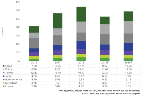
SAN FRANCISCO, Calif. – July 10, 2019 – Global sales of semiconductor manufacturing equipment by original equipment manufacturers are projected to drop 18.4 percent to $52.7 billion in 2019 from last year’s historic high of $64.5 billion, SEMI, the global industry association representing the electronics manufacturing and design supply chain, reported today in its Mid-Year Total Equipment Forecast.

semi-logo

Released at SEMICON West 2019, the forecast shows growth in equipment sales resuming in 2020, with an 11.6 percent jump to $58.8 billion. The current forecast reflects recent downward adjustments in capital expenditures and rising market uncertainty due in part to geopolitical tensions.

The SEMI Mid-Year Forecast shows wafer processing equipment sales falling 19.1 percent in 2019 to $42.2 billion. The other front-end segment, consisting of fab facilities equipment, wafer manufacturing, and mask/reticle equipment, is expected to slide 4.2 percent to $2.6 billion this year. The assembly and packaging equipment segment is on track to decline 22.6 percent to $3.1 billion in 2019, while semiconductor test equipment is forecast to decrease 16.4 percent to $4.7 billion this year.

Taiwan will dethrone Korea as the largest equipment market and lead the world with 21.1 percent growth this year, followed by North America with an 8.4 percent uptick. China will maintain the second spot for the second consecutive year, and Korea will fall to third after throttling back capital expenditures. All regions tracked except Taiwan and North America will contract this year.

SEMI forecasts that, in 2020, the equipment market is expected to recover on the strength of memory spending and new projects in China. Equipment sales in Japan will surge 46.4 percent to $9.0 billion. China, Korea, and Taiwan are forecast to remain the top three markets next year, with China rising to the top for the first time. Korea is forecast to become the second largest market at $11.7 billion, while Taiwan is expected to reach $11.5 billion in equipment sales. More upside is likely if the macroeconomy improves and trade tensions subside in 2020.

The Mid-Year Total Equipment Forecast is based on SEMI's industry-recognized World Fab Forecast database and input from equipment manufacturers. Total equipment includes wafer processing, other front end, total test, and assembly and packaging equipment.

 The following results are in terms of the market size in billions of U.S. dollars.

2019-Mid-Year-Forecast

The Equipment Market Data Subscription (EMDS) from SEMI provides comprehensive market data for the global semiconductor equipment market. A subscription includes three reports: the monthly SEMI Billings Report, which offers an early perspective of the trends in the equipment market; the monthly Worldwide Semiconductor Equipment Market Statistics (SEMS), a detailed report of semiconductor equipment bookings and billings for seven regions and over 22 market segments; and the SEMI Mid-Year Forecast, which provides an outlook for the semiconductor equipment market.

For more information or to subscribe, please contact SEMI customer service at 1.877.746.7788 (toll free in the U.S.). For more information online, please click here.

About SEMI

SEMI® connects more than 2,100 member companies and 1.3 million professionals worldwide to advance the technology and business of electronics design and manufacturing. SEMI members are responsible for the innovations in materials, design, equipment, software, devices, and services that enable smarter, faster, more powerful, and more affordable electronic products. Electronic System Design Alliance (ESD Alliance), FlexTech, the Fab Owners Alliance (FOA) and the MEMS & Sensors Industry Group (MSIG) are SEMI Strategic Association Partners, defined communities within SEMI focused on specific technologies. Visit www.semi.org to learn more, contact one of our worldwide offices, and connect with SEMI on LinkedIn and Twitter.

Association Contact

Michael Hall/SEMI

Phone: 1.408.943.7988

Email: [email protected]
SAN FRANCISCO, Calif. – July 1, 2019 – China’s Xpeng Motors will display and dissect an automotive unicorn – a rare, all-electric sports utility vehicle – at SEMICON West, July 9-11 at the Moscone Center. Also available for a look under the hood is General Motors’ self-driving Chevrolet Bolt Cruise AV Autonomous Test Vehicle, featuring no more steering wheel to clutter the cockpit.

SEMICON West Logo

Xpeng’s G3 Smart SUV rolled its 10,000th vehicle off the company’s Zhengzhou production line this month, while attaining top customer delivery numbers among new EV makers in China for 2019.

Loaded with microelectronics, including from among suppliers who will attend SEMICON West, the G3 comes equipped with smart autonomous driving and connectivity features, many of them first of their kind. Fully electric and seating five, the G3 features a voice-activated artificial intelligent assistant, driverless auto parking, heartbeat monitoring, facial recognition, a fatigue alert system and other utilization of new capabilities that rely on sophisticated electronics.

Like its future production model, the Chevy Bolt Cruise AV test vehicle to be displayed won’t have a steering wheel. As a replacement for that old-fashioned guiding mechanism, the vehicle is equipped with an advanced sensor program capable of reacting to its surrounding environment 360 degrees, day or night. Central to the vehicle’s command are computers using a combination of systems, including machine learning, dispatch and routing, remote assistance, simulation, planning and networking. It has been tested in one of the most complex driving environments in the U.S. – San Francisco.

The G3 and autonomous Bolt will be on display in the Smart Transportation Pavilion, which during SEMICON West’s three days also will feature Meet the Experts sessions for:

Media and visitors who want to view the vehicles and attend the conference can register here.

Platinum Sponsors for SEMICON West are Applied Materials, KLA, Lam Research and TEL. Other top sponsors are AEM Singapore, ASE, Burr & Forman LLP, Edwards, eSilicon Corporation, SAP and Silvaco.

Follow SEMICON West and the AI Design Forum on Twitter: @SEMIconex and #SEMICONWest, #AIDesignForum

About SEMI
SEMI® connects more than 2,100 member companies and 1.3 million professionals worldwide to advance the technology and business of electronics design and manufacturing. SEMI members are responsible for the innovations in materials, design, equipment, software, devices, and services that enable smarter, faster, more powerful, and more affordable electronic products. Electronic System Design Alliance (ESD Alliance), FlexTech, the Fab Owners Alliance (FOA) and the MEMS & Sensors Industry Group (MSIG) are SEMI Strategic Association Partners, defined communities within SEMI focused on specific technologies. Visit www.semi.org to learn more, contact one of our worldwide offices, and connect with SEMI on LinkedIn and Twitter.


Association Contact   

Scott Stevens, Cardinal Communications for SEMI Americas

Phone: 1.512.288.4050 

Email: [email protected]

MILPITAS, Calif. – July 1, 2019 – The SEMI Smart Manufacturing Initiative today released the semiconductor industry’s first Benchmark Survey to assess the current implementation level of automation and control measures aimed at increasing productivity and efficiency in front-end semiconductor fabs. Also designed to gauge the readiness of respondents to implement further smart manufacturing measures, the survey was distributed to more than 5,000 contacts across 200 companies that manage device fabrication facilities. The deadline for completing and returning the survey is July 26.

semi-logo

The Benchmark Survey will help participating members assess where their facilities fall on the smart manufacturing implementation curve using methodologies defined in the Overall Equipment Efficiency (OEE) SEMI Standard as a guide. Fab implementation of the technologies will be categorized by speed, output and quality – all top-level metrics of factory efficiency.

The Benchmark Project

The survey was created by subject matter experts from the Americas Chapter of the SEMI Smart Manufacturing Technology Community. Member companies include Intel, Applied Materials, EMD Performance Materials, MAX International Engineering Group, Cimetrix, Jabil and SUNY Polytechnic Institute. The group collaborated with Advanced Focus, a provider of services to improve manufacturing performance. Focusing on front-end semiconductor processing, the benchmark will later be extended to include the assembly, test, surface-mount and printed circuit board assembling sectors of the electronics industry.

“This survey benchmarks the current level of adoption and implementation of smart manufacturing technologies in the fab and how it affects manufacturing efficiency,” said Zsolt Marcet, supply chain engineer at Intel and current co-chair of the Benchmark Survey team. “It will give valuable insights into the industry as a whole in understanding the role of smart manufacturing.”

“OEE provides an effective metric of how a fab is performing in the transition to smart manufacturing,” said Dinesh Saigal, senior manager at Applied Materials and also co-chair of the Benchmark Survey team.

smart-manufacturing

“This study is unprecedented in demonstrating how smart manufacturing is a differentiator in factory performance,” said Ariel Meyuhas, COO of MAX International Engineering Group and a Benchmark Survey team member. “It will give participants an excellent view of what peers are doing to improve fab efficiency and competitiveness using smart manufacturing metrics.”

“The team SEMI assembled to develop this groundbreaking Benchmark Survey consists of major industry players with deep expertise in factory automation,” said Tom Salmon, vice president of Collaborative Technology Platforms at SEMI and leader of the Smart Manufacturing Initiative. “We look forward to leveraging the survey results to design best practices and guidelines across the electronics manufacturing supply chain and drive the adoption of AI, ML and predictive analytic solutions that fulfill the promise of smart manufacturing.”

IDMs or foundries interested in completing the survey can click here to request a link.

The Smart Manufacturing Pavilion is among the theme pavilions featured at SEMICON West, July 9-11 at the Moscone Center in San Francisco.  

About the Smart Manufacturing Initiative
The SEMI Smart Manufacturing Initiative involves experts from the full supply chain including equipment and materials providers, device makers, OSATs, printed circuit board assemblers and software providers. The initiative is designed to identify gaps in smart manufacturing across the supply chain and drive the implementation of automation, control, increase productivity, yield enhancement and overall efficiency along with the application of other smart manufacturing technologies.

About SEMI
SEMI® connects more than 2,100 member companies and 1.3 million professionals worldwide to advance the technology and business of electronics design and manufacturing. SEMI members are responsible for the innovations in materials, design, equipment, software, devices, and services that enable smarter, faster, more powerful, and more affordable electronic products. Electronic System Design Alliance (ESD Alliance), FlexTech, the Fab Owners Alliance (FOA) and the MEMS & Sensors Industry Group (MSIG) are SEMI Strategic Association Partners, defined communities within SEMI focused on specific technologies. Visit www.semi.org to learn more, contact one of our worldwide offices, and connect with SEMI on LinkedIn and Twitter.

Association Contact

Michael Hall/SEMI
Phone: 1.408.943.7988
Email: [email protected]



SEMICON West Logo

MILPITAS, Calif. – July 1, 2019 – SEMI and Semiconductor Digest today announced finalists for the Best of West award to be presented at SEMICON West 2019, July 9-11 at the Moscone Center in San Francisco. Presented by SEMI and Semiconductor Digest each year, the Best of West award recognizes innovative new products or services that are significantly advancing the electronics manufacturing supply chain or a particular manufacturing capability.

Selected from over 500 exhibitors, the following Best of West 2019 finalists will showcase their products on the show floor at SEMICON West 2019.

CyberOptics: NanoResolution MRS Sensor        

CyberOptics Logo

Proprietary MRS sensor technology, deemed best-in-class, enables metrology-grade accuracy by inhibiting optical measurement distortions and reflections. CyberOptics’ unique sensor architecture simultaneously captures and transmits multiple images in parallel while proprietary 3D fusing algorithms merge the images. The result is ultra-high quality 3D images and high-speed inspection.


Advantest: V93000 Wave Scale Millimeter Solution        

Advantest

The dawning of 5G and 5G-NR (new radio) ICs requires test equipment to handle millimeter-wave (mmWave) frequencies. Advantest’s scalable V93000 Wave Scale™ RF solution has been extended to support multi-band testing at the fast interface speeds used by 5G devices, making it the industry’s first fully integrated, multi-site mmWave ATE test solution.


Edwards: Atlas System       

Edwards Logo 270 px

Edwards’ innovative porous head/slot nozzle technology, combined with its unique inward fired combustor, is designed to manage PFC abatement and high-flow flammable process gas in the pump exhausts. In addition, when embedded into Edwards’ sub-fab integrated solution, it reduces customer risk and improves customers’ uptime.

Congratulations to each of the Finalists. The Best of West Award winner will be announced during SEMICON West on Wednesday, July 10, 2019.

More than 23,000 professionals from the electronics manufacturing supply chain are expected to attend SEMICON West, the flagship event for the U.S. semiconductor industry. Learn more at www.semiconwest.org.

Platinum Sponsors for SEMICON West are Applied Materials, KLA, Lam and TEL, plus other top sponsors AEM Singapore, ASE, Burr & Forman LLP, Edwards, eSilicon Corporation, SAP and Silvaco. More information is available on the SEMICON West 2019 website. Follow SEMICON West and the AI Design Forum on Twitter: @SEMIconex – #SEMICONWest, #AIDesignForum

About Semiconductor Digest

Through a mix of news, contributed articles and staff-written articles, Semiconductor Digest is dedicated to providing global information about the design, manufacturing, packaging and testing of semiconductors and other types of electronic devices, including MEMs, LEDs, displays, power electronics, optoelectronics/photonics, biomedical devices, solar cells, thin film batteries and flexible electronics. Semiconductor Digest consists of a website, magazine and topic-focused newsletters.

About SEMI

SEMI® connects more than 2,100 member companies and 1.3 million professionals worldwide to advance the technology and business of electronics design and manufacturing. SEMI members are responsible for the innovations in materials, design, equipment, software, devices, and services that enable smarter, faster, more powerful, and more affordable electronic products. Electronic System Design Alliance (ESD Alliance), FlexTech, the Fab Owners Alliance (FOA) and the MEMS & Sensors Industry Group (MSIG) are SEMI Strategic Association Partners, defined communities within SEMI focused on specific technologies. Visit www.semi.org to learn more, contact one of our worldwide offices, and connect with SEMI on LinkedIn and Twitter.

Association Contacts

Michael Hall/SEMI
Phone: 1.408.943.7988
Email: [email protected]

Scott Stevens, Cardinal Communications for SEMI Americas
Phone: 1.512.288.4050
Email: [email protected]


Semiconductor Digest Contact
Pete Singer, Editor-in-Chief
Phone: 1.978.470.1806
Email: [email protected]

Milpitas, Calif. – June 27, 2019 – SEMI today announced a research and development (R&D) project to speed technology progress and problem-solving in microelectronics manufacturing and across the supply chain by driving new efficiencies using machine learning (ML) and artificial intelligence (AI). Under an agreement with SEMI, Cornell University will optimize and accelerate two critical process steps – lithography and plasma etch. Supported through SEMI’s R&D program with the U.S. Army Research Laboratory (ARL), the project aims to help accelerate the adoption of data-driven AI methodologies to streamline microelectronics operations.

semi-logo

The project will lay the foundation for SEMI to establish data transfer and management standards crucial to the trusted exchange of trade secrets, IP and other sensitive information. New standards and protocols are vital as the industry moves into the era of big data.

Semiconductor manufacturing is extremely complex due to the intricate interdependencies among various processes, environments, tools, and materials. This complexity deepens with the rise of new technologies and makes existing analytical approaches such as statistical process control (SPC) and design of experiments (DOE) more challenging. In addition, analyzing cleanroom data is now harder because of varying formats and lack of physical models for categorizing the data. Consequently, identifying root causes of manufacturing problems is much more difficult, slowing the development of new technologies.

“Streamlining manufacturing processes across the microelectronics supply chain to address the rising complexity of technology development is key for the industry to keep pace with market demand and drive growth,” said Ajit Manocha, SEMI president and CEO. “The microelectronics industry has been slow to adopt ML and AI due, in part, to IP and data security concerns that impede data-sharing. SEMI’s agreement with Cornell, supported by ARL, is an important step in using ML and AI techniques to tackle this and other issues and bring new technologies to market faster.”

Tools and materials from several SEMI members will be used for the project at Cornell University’s NanoScale Science & Technology Facility (CNF).

The budget for the year-long project is provided by the ARL grant, SEMI, and through in-kind contributions from companies in the form of materials and testing services. The principal investigators from Cornell University are Dr. Christopher K. Ober, professor of Materials Engineering and Director of the CNF, and Dr. Amit Lal, professor in the School of Electrical and Computer Engineering. Dr. Peter Doerschuk, Dr. Ed Suh, and Dr. Don Tennant will also support the project with expertise spanning computer systems, high-performance software and facilities management.


About SEMI

SEMI® connects more than 2,100 member companies and 1.3 million professionals worldwide to advance the technology and business of electronics design and manufacturing. SEMI members are responsible for the innovations in materials, design, equipment, software, devices, and services that enable smarter, faster, more powerful, and more affordable electronic products. Electronic System Design Alliance (ESD Alliance), FlexTech, the Fab Owners Alliance (FOA) and the MEMS & Sensors Industry Group (MSIG) are SEMI Strategic Association Partners, defined communities within SEMI focused on specific technologies. Visit www.semi.org to learn more, contact one of our worldwide offices, and connect with SEMI on LinkedIn and Twitter.


Association Contact

Michael Hall
Phone: 1.408.943.7988
Email: [email protected]



What to Make of the ‘Quantum Advantage’ at SEMICON West?

  • IBM demos its model of the bleeding-edge Q Computer, while the Quantum Economic Development Consortium lays out first steps toward creation of a Quantum Industry Roadmap
  • Dean Kamen introduces quantum leaps for enabling large-scale replacement of human organs
  • New additions to the already announced top-shelf keynotes feature Nate Baxter of TEL, Oreste Donzella of KLA, Victor Peng of Xilinx, Dr. Lisa Su of AMD and Aart de Geus of Synopsys
  • AI Design Forum™ returns to explore “The Future of Computing – from Materials to Systems,” as Electronic Systems Design Alliance co-locates for the first time with SEMICON West

MILPITAS, Calif. – June 25, 2019 – SEMICON West participants will gain first look at Quantum Economic Development Consortium (QED-C) roadmapping activities devoted to the pursuit of U.S. leadership in the rapidly emerging global quantum industry – as well as live demonstrations of IBM’s Q Computer model, which showcases quantum computing architecture built upon decades of semiconductor industry advances. Markets that soon may claim staggering leaps from a quantum computational capacity span from automotive to medical, financial and energy.

SEMICON West Logo

This opportunity to gauge the impact and timing of quantum advantage on applications for sensing, communication and computing, as well as the opportunities and demands for the microelectronics supply chain, will be among highlights at the 49th SEMICON West, July 9-11 at San Francisco’s Moscone Center.

Boeing and IBM, as well as pure-play quantum companies Zapata Computing and QCWare and more than 50 other U.S. companies from across the quantum supply chain, have joined the QED-C. The consortium – recently launched with support from the U.S. Department of Commerce’s National Institute of Standards and Technology (NIST) and industry, and managed by SRI International – aims to enable and grow the U.S. commercial quantum industry. Among the many next-generation technologies to be featured, SEMICON West will host a TechTALK where QED-C and industry leaders will detail quantum opportunities – from software to manufacturing. 

Also addressing the promise of quantum advancements will be SEMICON West keynote Dean Kamen, founder of DEKA Research and Development and a legendary inventor, who will explore the leading edge in biofabrication of human organs. Called a “modern-day Edison” by Fortune magazine, Kamen noted “The world needs a quantum leap in the ability to replace body organs, which is where we’re going. And we’re united philosophically with SEMI on the need and effort to cultivate the next wave of talent that’ll help take us there and beyond.”

Prior to their TechTALK, QED-C will be among a select set of news presenters and economic forecasts at the West View Media Lunch and News Conference on Tuesday, July 9.


New SEMICON West Keynotes

Nate-Baxter
Nate Baxter, general manager of Tokyo Electron’s U.S. Development and production group, will address What Does Innovation Look Like in the Era of Industry 4.0.  
TEL
Oreste-Donzella
Oreste Donzella, KLA senior vice president of Global Customer Solutions and Chief Marketing Officer, will speak on Trends in Automotive: The Changing Role of Fab Inspection and Metrology in ‘Zero Defect.’
KLA
Victor-Peng
Victor Peng, Xilinx President and CEO, will present entirely new silicon and software platforms for AI Era applications, designed to deliver order-of-magnitude improvements in performance and performance per watt.   
XILINX

A complete list of keynotes and executive panels is available online. So is information about topics and speakers for the AI Design Forum: The Future of Computing – from Materials to Systems, 9:15 a.m. - 4:40 p.m. Tuesday, July 9.

As SEMI and the Electronic System Design Alliance evolve to move the industry forward, ES Design West will co-locate with SEMICON West. Platinum Sponsors for SEMICON West are Applied Materials, KLA, Lam Research and TEL. Other top sponsors AEM Singapore, ASE, Burr & Forman LLP, Edwards, eSilicon Corporation, SAP and Silvaco.

SEMICON West is the culmination of eight progressive conferences that comprise SEMI’s inaugural Technology Leadership Series of the Americas. More information is available on the SEMICON West 2019 website.

Follow SEMICON West and the AI Design Forum on Twitter: #SEMICONWest, #AIDesignForum and @SEMIconex

About SEMI    

SEMI® connects more than 2,100 member companies and 1.3 million professionals worldwide to advance the technology and business of electronics design and manufacturing. SEMI members are responsible for the innovations in materials, design, equipment, software, devices, and services that enable smarter, faster, more powerful, and more affordable electronic products. Electronic System Design Alliance (ESD Alliance), FlexTech, the Fab Owners Alliance (FOA) and the MEMS & Sensors Industry Group (MSIG) are SEMI Strategic Association Partners, defined communities within SEMI focused on specific technologies. Visit www.semi.org to learn more, contact one of our worldwide offices, and connect with SEMI on LinkedIn and Twitter.


Association Contact   

Scott Stevens, Cardinal Communications for SEMI Americas

Phone: 1.512.288.4050 

Email: [email protected]

MILPITAS, Calif. — June 20, 2019 — North America-based manufacturers of semiconductor equipment posted $2.06 billion in billings worldwide in May 2019 (three-month average basis), according to the May Equipment Market Data Subscription (EMDS) Billings Report published today bySEMI.The billings figure is 7.4 percent higher than the final April 2019 level of $1.92 billion, and is 23.6 percent lower than the May 2018 billings level of $2.69 billion.

SEMI

“Billings of North American equipment manufacturers increased for the second consecutive month,” said Ajit Manocha, president and CEO of SEMI. “Expanding end-market applications continue to fuel demand for advanced semiconductors and the equipment necessary to manufacture those devices. However, market volatility continues due to the macroeconomic environment.”

The SEMI Billings report uses three-month moving averages of worldwide billings for North American-based semiconductor equipment manufacturers. Billings figures are in millions of U.S. dollars.


Billings
(3-mo. avg.)

Year-Over-Year

December 2018

$2,104.0

-12.3%

January 2019

$1,896.3

-20.0%

February 2019

$1,868.1

-22.7%

March 2019

$1,825.3

-24.9%

April 2019 (final)

$1,922.0

-28.5%

May 2019 (prelim)

$2,064.0

-23.6%

Source: SEMI (www.semi.org), June 2019

SEMI publishes a monthly North American Billings report and issues the Worldwide Semiconductor Equipment Market Statistics (WWSEMS) report in collaboration with the Semiconductor Equipment Association of Japan (SEAJ). The WWSEMS report currently reports billings by 24 equipment segments and by seven end market regions. SEMI also has a long history of tracking semiconductor industry fab investments in detail on a company-by-company and fab-by-fab basis in its World Fab Forecast and SEMI FabView databases. These powerful tools provide access to spending forecasts, capacity ramp, technology transitions, and other information for over 1,000 fabs worldwide. For an overview of available SEMI market data, please visit www.semi.org/en/MarketInfo.

The data contained in this release were compiled by David Powell, Inc., an independent financial services firm, without audit, from data submitted directly by the participants. SEMI and David Powell, Inc. assume no responsibility for the accuracy of the underlying data.


About SEMI
SEMI® connects more than 2,100 member companies and 1.3 million professionals worldwide to advance the technology and business of electronics design and manufacturing. SEMI members are responsible for the innovations in materials, design, equipment, software, devices, and services that enable smarter, faster, more powerful, and more affordable electronic products. Electronic System Design Alliance (ESD Alliance), FlexTech, the Fab Owners Alliance (FOA) and the MEMS & Sensors Industry Group (MSIG) are SEMI Strategic Association Partners, defined communities within SEMI focused on specific technologies. Visit www.semi.org to learn more, contact one of our worldwide offices, and connect with SEMI on LinkedIn and Twitter.

Association Contact
Michael Hall/SEMI
Phone: 1.408.943.7988
Email: [email protected]

Notes
Next SEMI Billings report is July 23, 2019 at 3:00pm Pacific 
For information on SEAJ Book-to-Bill Report, visit www.seaj.or.jp

GRENOBLE, France – June 19, 2019 – With MEMS and imaging sensor innovations driving an explosion of transportation, medical, mobile, industrial and other Internet of Things (IoT) applications, the stage is set for the SEMI MEMS & Imaging Sensors Summit, 25-27 September 2019 at the World Trade Center (WTC) in Grenoble, France. More than 400 industry experts are expected to gather for insights on the latest developments and trends across the supply chain. Registration is open now with early-bird pricing available until August 17, 2019.

MEMS & Imaging Sensors Summit Logo

System integration success stories and the industry’s response to growing demand for data harvesting and analytics with new Artificial Intelligence (AI) capabilities will highlight the event.

The summit will open with executive keynotes and feature MEMS and Sensors and the Imaging and Sensors tracks over the following two days.

Speakers Include

Antti Vasara Photo

Antti Vasara, President and CEO at VTT Ltd., will explore sensor fusion, AI and new technological developments that enable new solutions to global challenges and new business opportunities in his opening day executive keynote.

VTT Logo


Alexis Bernard Photo

Alexis Bernard, CTO at Knowles, will discuss how the explosion of voice, audio and sound in a wide range of devices is creating new user experiences and how consumers interact with devices more intuitively.

Knowles Logo


Gaetano D'Aquila Photo

Gaetano D'Aquila, Co-founder and CEO at GiPStech, will present a technology that uses a commercial smartphone or other Smart hardware for effective, precise localization in indoor settings in the absence of an adequate GPS signal.

GiPStech Logo


Dr. Markus Sonnemann Photo

Dr. Markus Sonnemann, VP of Engineering MEMS at Bosch Automotive Electronics, will explore requirements for new MEMS use cases and how to manage rising complexity while providing examples of successful implementation of MEMS solutions in new applications.

Bosch Logo

Other Highlights

  • MEMS and Imaging Technology Showcase – Several companies will stage live demonstrations of their products powered by MEMS, imaging and sensors devices as they compete for audience votes.
  • The Joint Show Floor Exhibition is the place to see leading companies, technologies, and innovators driving the future of MEMS/imaging and sensors design and manufacturing.
  • Networking events such as the welcome reception and a gala dinner for both MEMS and Sensors and Imaging & Sensors Summit attendees.

Stay in Touch on Twitter @SEMIEurope

  • #SensorsSummit #MEMS #Imaging #IoT #AI #SEMIEurope

Premier sponsors

For more information including the full event agenda, please visit the MEMS & Sensors Imaging Summit website.

About SEMI

SEMI® connects more than 2,100 member companies and 1.3 million professionals worldwide to advance the technology and business of electronics design and manufacturing. SEMI members are responsible for the innovations in materials, design, equipment, software, devices, and services that enable smarter, faster, more powerful, and more affordable electronic products. Electronic System Design Alliance (ESD Alliance), FlexTech, the Fab Owners Alliance (FOA) and the MEMS & Sensors Industry Group (MSIG) are SEMI Strategic Association Partners, defined communities within SEMI focused on specific technologies. Visit www.semi.org to learn more, contact one of our worldwide offices, and connect with SEMI on LinkedIn and Twitter.

Press Contact
Serena Brischetto/SEMI Europe
Email: [email protected]
MILPITAS, Calif. — June 11, 2019 — Global fab equipment spending will rebound in 2020, growing 20 percent to US$58.4 billion after dropping 19 percent to US$48.8 billion in 2019, according to the Q2 2019 World Fab Forecast update published by SEMI, the global industry association representing the electronics manufacturing and design supply chain.

semi-logo

The 2020 investment increase is a downward revision from the 27 percent growth forecast earlier this year, and the 19 percent drop in 2019 spending is deeper than the previously projected decline of 14 percent. Despite the healthy gains forecast for 2020, fab spending will still fall $2 billion short of 2018 investments.

Memory sector spending alone is expected to account for a disproportionate share of the 2019 falloff, dropping 45 percent, but should stage a strong recovery of 45 percent to US$28 billion in 2020. The 2020 increase in memory investments would mark year-over-year growth of more than US$8 billion and drive an overall expansion in fab spending. However, compared to 2017 and 2018 spending levels, 2020 memory investments will be considerably less if the forecast holds.

In two countertrends to the memory spending falloff this year, foundry sector investments are projected to increase by 29 percent, with micro growing by over 40 percent, fueled by the 10nm MPU launch. It’s important to note that overall micro spending is dwarfed by foundry and memory investments.

The World Fab Forecast update tracks investment projects of 440 fabs and lines from 2018 to 2020. A review of the SEMI data by half year (Figure 1) shows that memory spending will drop 48 percent in the first half of 2019, with investments in sector components 3D NAND and DRAM plunging 60 percent and 40 percent, respectively.

Fab equipment spending by half year from 2018 to 2020

Figure 1: Fab equipment spending by half year from 2018 to 2020


Despite this staggering drop in one sector, overall spending in the first half of 2019 will be partially offset by a 40 percent increase in investments by leading foundries. With MPU its key driver, micro spending is expected to grow 16 percent in the first half of the year and another 9 percent in the second half.

The SEMI World Fab Forecast report covers new, planned and existing fabs as well as fab spending for construction and equipping, capacity expansion, and technology nodes by quarter and by product type with more than 1,300 front-end fab listings. Since its previous publication in February 2019, 192 updates have been made to the report including the addition of 14 new facilities and lines.

Learn more about SEMI fab databases at www.semi.org/en/MarketInfo/FabDatabase.  

About SEMI

SEMI® connects more than 2,100 member companies and 1.3 million professionals worldwide to advance the technology and business of electronics design and manufacturing. SEMI members are responsible for the innovations in materials, design, equipment, software, devices, and services that enable smarter, faster, more powerful, and more affordable electronic products. Electronic System Design Alliance (ESD Alliance), FlexTech, the Fab Owners Alliance (FOA) and the MEMS & Sensors Industry Group (MSIG) are SEMI Strategic Association Partners, defined communities within SEMI focused on specific technologies. Visit www.semi.org to learn more, contact one of our worldwide offices, and connect with SEMI on LinkedIn and Twitter.

Association Contact
Michael Hall/SEMI
Phone: 1.408.943.7988
Email: [email protected]