SEMI Members: $75
Use your corporate email address during log in to be recognized as a SEMI Member.
Non-Members: $149
Students: Free
Contact Basak Ulutas Ozturkler ([email protected]) with a picture of your student ID to receive your discount code.
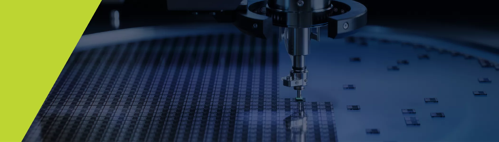
Digital Twin is a virtual representation of the structure, context, and behavior of physical systems or a process, with a live link to a physical system serving as a key enabler for predictive and data-driven optimization. In Printed and Flexible Hybrid Electronics (FHE), manufacturing involves multiple interdependent variables—different printing technologies, inks, substrates, and process conditions—each introducing its own complexity. In practice, additional challenges such as equipment drift, batch-to-batch variations, and environmental fluctuations further impact process consistency and yield. Changing a process or transferring it between tools is often difficult, as each setup is highly customized and sensitive to local conditions. To address these challenges, Digital Twin frameworks connect data from design, fabrication, and metrology into continuously learning digital models. They enable early detection of process drifts, virtual experimentation for process development, and data-driven optimization that reduces time, cost, and waste.
This course introduces Digital Twin frameworks for FHE, focusing on Deep Neural Network (DNN)-based predictive models. Participants will learn how to integrate design, fabrication, and metrology data into continuously learning virtual twins that detect process drifts, enable virtual experimentation, and optimize manufacturing. The program covers the full workflow—from image processing and virtual metrology to AI model training, validation, and hyperparameter tuning—using real datasets. A hands-on “Build Your Own Digital Twin” module in Google Colab will provide practical experience in training and refining models for printed electronics applications, equipping attendees with both theoretical insight and applied skills for process optimization and performance prediction.
ABOUT THE SPEAKER
Benyamin Davaji, PhD
Benyamin Davaji is an Assistant Professor in the Department of Electrical and Computer Engineering at Northeastern University, Boston, Massachusetts, where his research centers on integrated microsystems for sensing and computation using mechanical waves. His work spans acoustic and ultrasound transducers, biointerfaces, and microcalorimetry, with a strong emphasis on data-guided nanofabrication, advanced semiconductor device manufacturing, and interdisciplinary approaches to microsystem design and manufacturing. He earned his Ph.D. in Electrical and Computer Engineering from Marquette University in 2016 and completed a postdoctoral appointment at Cornell University.
United States


Join us for a Master Class with Benyamin Davaji, PhD, as he introduces Digital Twin frameworks for Printed and Flexible Hybrid Electronics, demonstrating how AI- and DNN-based models integrate design, fabrication, and metrology data along with printing technologies to detect process drift, enable virtual experimentation, and optimize manufacturing performance. Participants gain hands-on experience building continuously learning digital twins to reduce variability, cost, and time to optimization.