downloadGroupGroupnoun_press release_995423_000000 copyGroupnoun_Feed_96767_000000Group 19noun_pictures_1817522_000000Member company iconResource item iconStore item iconGroup 19Group 19noun_Photo_2085192_000000 Copynoun_presentation_2096081_000000Group 19Group Copy 7noun_webinar_692730_000000Path
Skip to main content
Default Banner Image

India

China India Japan Malaysia Singapore Taiwan Vietnam Chiplet & Heterogeneous 6/30 Training

Course Description 

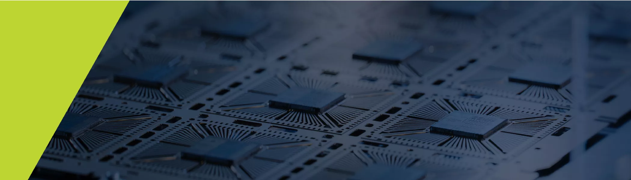
This workshop reviews the needs of the packaging solution to meet the demand for digitalization through the artificial intelligent and Internet-of-things from urbanization, sustainability to industry. The course provides an overview of the fabrication process of IC carriers of leadframe, ceramics, substrate and flex and how they have to evolve to meet the heterogeneous integration. With these foundations, various stacking and integration technologies through wirebonding, flip chip and 3D interconnect from interconnect to system level will be shared. Packaging innovation of TSV, fan-in, fan-out wafer level packaging and its challenges will also be shared for chiplet and heterogeneous integration. It ends off by sharing the embedded technologies and embedded multi-die interconnect bridge for chiplet and heterogeneous integration.

The course looks into the R&D development as well as the dynamics changes of heterogeneous integration technologies in the Semiconductor packaging arena. This workshop curates the technologies development to date and provides the necessary information for professionals in the manufacturing and R&D environment to perform their tasks.

Who Should Attend

This course is intended for both manufacturing and R&D know-how in IC packaging professionals, including but not limited to:

  • Directors
  • Managers
  • Process Engineers
  • R&D Engineers
  • Sales and Application Engineers who supply packaging materials and tools

Learning Objectives

  • Understand why chiplet and heterogeneous integration for advanced packaging
  • Review of IC carriers
  • Summarize 3D and TSV for Chiplet and Heterogeneous Integration
  • Explain Fan-in and Fan-out wafer-level packaging for chiplet and heterogeneous integration
  • Describe chiplet, embedded, and embedded multi-die interconnect beam for chiplet and glass substrate for heterogenous integration 

Instructor

Dr. Lee Teck Kheng

Institue of Technical Education

Instructor Bio

Testimonials 

See what previous course participants had to say about this training!

  • "All the necessary information are neatly fitted into a few slides prepared by Dr. Lee"
  • "I found the review of the material between sessions and the slides to follow along with to be the most beneficial aspects of the training."
  • "Much thanks to Dr. Lee & SEMI University for giving me a chance to study all my unclear items in the past."

Important Information

Note that only the person who registered will receive a certificate of completion. This virtual training will not be recorded. Attendees must be present to access course knowledge. 

Can't find the training link day of? After you register, you will receive the link to the live training via the email address you provided. In addition, you will receive email reminders about 24 hours in an advance and an hour before with the same link. Please keep these emails on hand to access the trainings on time. If you do not see any confirmation emails, please check your junk/spam folders before contacting SEMI U for support.

Singapore

SEMI U

Chiplet and heterogeneous integration of packaging has been embraced as the next revolutionary innovation to meet the quest of size, cost, and performance for packaging. The technologies are seen as another disruptive technology to bring devices into a package by integrating the various Multi-chip module (MCM), 3D packaging, Through Silicon Via (TSV), and Fan-out wafer level packaging (Fo-WLP) technologies into a system in the package for applications. Chiplet, EMIB, and glass substrate will also be shared in this course. 

Pricing
  • Members: $599
  • Non-Members: $649

* For group orders with 10+ attendees, and for Students/Veterans discounted pricing, please contact [email protected]

8:30 am - 5:00 pm Off Add to Calendar 2026-06-30 08:30:00 2026-06-30 17:00:00 Chiplet and Heterogeneous Integration for Microelectronics Packaging (Asia) Chiplet and heterogeneous integration of packaging has been embraced as the next revolutionary innovation to meet the quest of size, cost, and performance for packaging. The technologies are seen as another disruptive technology to bring devices into a package by integrating the various Multi-chip module (MCM), 3D packaging, Through Silicon Via (TSV), and Fan-out wafer level packaging (Fo-WLP) technologies into a system in the package for applications. Chiplet, EMIB, and glass substrate will also be shared in this course. PricingMembers: $599Non-Members: $649* For group orders with 10+ attendees, and for Students/Veterans discounted pricing, please contact [email protected] Singapore SEMI.org [email protected] Asia/Singapore public Asia/Singapore Register Now
Event format
Promote in calendar
Off

Registration Details

Registration is required for this event as it is likely to reach maximum room capacity, at which point interested attendees will be waitlisted.

SEMI Members:  $150

Non-Members of SEMI:  $200

Refunds possible before May 1, 2026.  Substitutions allowed up to May 20.

Questions? Contact James Amano at [email protected].

Belgium China France Germany India Ireland Italy Japan Singapore South Korea Taiwan United States 2026 EHS Summit Banner Business Executive Technical

The Summit includes strategic business and technical information for many levels and sectors of the ecosystem, including:

  • Government relations/advocacy staff
  • EHS regulatory professionals
  • Senior executives
  • Business development
  • Device manufacturers
  • Equipment suppliers
  • Materials suppliers
  • Component suppliers
  • Fab and facility systems construction companies

SEMI
673 South Milpitas Blvd.
Milpitas, CA 95035
United States

8:30 am

Badge Pickup and Networking

9:00 am
Joe Stockunas
Joe Stockunas
President, SEMI Americas
SEMI

Welcome and Introduction

9:05 am
James Amano
James Amano
Senior Director, EHS
SEMI

SEMI EHS Overview

9:20 am
Russ Lamotte
K. Russell LaMotte
Principal
Beveridge & Diamond, PC

US Regulatory Landscape: PFAS, PIP, TTR, and more

9:50 am
Iranda Chaki
Iranda Chaki
Senior Policy Coordinator
SEMI Europe

Europe: PFAS Restriction, POPs, F-Gas, GENESIS, REACH

10:15 am

Break

10:45 am
Michael Golden
Michael Golden
Director, Navy Programs & Microelectronics Initiatives
Office of the Deputy Assistant Secretary of War for Product Support

US Department of War Perspective on Semiconductor Supply Chain Risks

11:15 am
Patrick Gottsacker
Patrick Gottsacker
Supply Chain Regulatory Compliance Program Manager
Intel

US EPA: TSCA New Substances of Concern

11:45 am

Morning Session Q&A

12:15 pm

Lunch & Networking

1:15 pm
James Amano
James Amano
Senior Director, EHS
SEMI

Review of afternoon agenda

1:20 pm
Andrew Petraszak
Andrew Petraszak
Tokyo Electron
Patrick Gottsacker
Patrick Gottsacker
Intel

PFAS Transparency

1:50 pm
Masahide Yodogawa
Masahide Yodogawa
Director, Technology Co-Creation Promotion Group
AGC, Inc.

PFAS Recycling

2:15 pm
Ben Kallen
Ben Kallen
Sr. Manager, Public Policy & Advocacy
SEMI
Andrew Petraszak
Andrew Petraszak
Tokyo Electron

SEMI Washington DC Update: Federal and State-level Advocacy

2:40 pm

Afternoon Q&A

3:00 pm - 3:30 pm

Networking

EHS Sustainability Standards

Plan now to join fellow semiconductor industry professionals at SEMI Headquarters in Milpitas, California at the 2026 SEMI EHS Summit.

Industry experts will present on the regulatory matters that will impact the industry in 2026 and beyond, followed by discussions on taking collective action to strengthen semiconductor manufacturing. 

Topics:

  • US Regulatory Landscape under second Trump Administration
  • US State-level legislation
  • Europe: PFAS restriction, REACH restriction, Packaging and Packaging Waste Regulation, GENESIS Consortium, etc.
  • US Department of War Perspective on Semiconductor Supply Chain Risks
  • Stockholm Convention
  • Emerging regulations in Asia
  • Supply Chain Transparency
  • US EPA Technology Transition Rule (HFC Phasedown)
  • US EPA TSCA New Substances of Concern

Attend, network and strategically prepare your company.  This is an in-person event only.

8:30 am - 3:30 pm Off Add to Calendar 2026-05-28 08:30:00 2026-05-28 15:30:00 2026 EHS Summit Plan now to join fellow semiconductor industry professionals at SEMI Headquarters in Milpitas, California at the 2026 SEMI EHS Summit.Industry experts will present on the regulatory matters that will impact the industry in 2026 and beyond, followed by discussions on taking collective action to strengthen semiconductor manufacturing. Topics:US Regulatory Landscape under second Trump AdministrationUS State-level legislationEurope: PFAS restriction, REACH restriction, Packaging and Packaging Waste Regulation, GENESIS Consortium, etc.US Department of War Perspective on Semiconductor Supply Chain RisksStockholm ConventionEmerging regulations in AsiaSupply Chain TransparencyUS EPA Technology Transition Rule (HFC Phasedown)US EPA TSCA New Substances of ConcernAttend, network and strategically prepare your company.  This is an in-person event only. SEMI 673 South Milpitas Blvd. Milpitas, CA 95035 United States SEMI.org [email protected] America/Los_Angeles public America/Los_Angeles Register Now
Event format
Promote in calendar
On
Belgium China France Germany India Ireland Italy Japan Malaysia Singapore South Korea Taiwan United States Watch the recording ICP 2026 2 Business Executive Technical
Highlighted content

United States

Sustainability

SEMI Sustainability, in collaboration with STX Group, hosted a webinar on Internal Carbon Pricing (ICP) for the semiconductor value chain. The session was anchored in a new industry report developed with input from members of SEMI’s Carbon Pricing Workgroup and will feature speakers from ASML, Delta Electronics, and Lam Research.  The webinar  highlighted the 5 key steps in creating and implementing your own ICP plan, and understand the process, its benefits and the opportunities offered.

The presentations explored key insights from the report alongside SEMI member perspectives, with speakers sharing practical examples and lessons learned—from early exploration to applied approaches—across the semiconductor value chain. 

Off Add to Calendar Disabled America/Los_Angeles
Event format
Promote in calendar
Off

Oxford Instruments, a leading provider of advanced plasma processing solutions, today announced a plasma equipment supply agreement with Applied Optoelectronics Inc. (AOI) (Nasdaq: AAOI), a leading provider of advanced optical and hybrid fibre-coaxial networking products that power the internet, for several etch and deposition cluster systems at their facility in Sugar Land, Texas.

The agreement will support AOI’s transformative expansion and technological advancements in indium phosphide (InP) for optoelectronic device manufacturing, as the company rapidly scales to increase production capacity within the U.S.

As AOI undergoes a significant growth phase, the company is upgrading its production capabilities to meet increasing demand for high-performance InP optoelectronic devices. Oxford Instruments’ advanced plasma etch and deposition processing systems will play a key role in this transformation by supporting AOI with fully automated 3-4-6-inch capable production systems for InP processes.

“AOI is expanding its U.S. manufacturing capacity in Texas to support demand for our optical transceivers in AI datacentres, and key suppliers like Oxford Instruments will help us continue to upgrade our fully automated production line,” said Fred Chang, Senior Vice President and North American General Manager at AOI. “With our combined technology, we can speed the processing of multiple wafer sizes, ranging from 3 to 6 inches, while improving overall quality and reducing costs.”

“AOI has been a valued long-term partner, and we are thrilled to have earned their trust as the chosen supplier for their production expansion and technology upgrades. Our unique high-temperature Electrostatic Chuck (ESC) design, which enables advanced processing capabilities, was a key factor in their decision. AOI also conducted an extensive vendor qualification process, including a visit to our brand-new purpose-built manufacturing facility in Bristol, UK, where we received high praise for our technology and production capabilities,” said Emiel Thijssen, Vice President of Sales and Business Development USA, Oxford Instruments Plasma Technology. “We are also investing significantly to ensure we continue to deliver world-class service capability in the Texas region, focusing on the availability of spares and expanding our field service and process engineering teams, to support the rapid expansion of leading manufacturers in the region such as AOI.”

###


For media enquiries, please contact:
Grant Baldwin, Head of Marketing
Oxford Instruments Plasma Technology
E: [email protected]
About Oxford Instruments plc
Oxford Instruments provides academic and commercial organisations worldwide with market-leading scientific technology and expertise across its key market segments: Materials Analysis, Healthcare & Life Science and Semiconductors. Innovation is the driving force behind Oxford Instruments' growth and success, supporting its core purpose to accelerate the breakthroughs that create a brighter future for our world. The vigorous search for new ways to make our world greener, healthier and more productive is driving unprecedented levels of R&D investment in new materials and techniques to support productivity and decarbonisation worldwide, creating a significant opportunity for Oxford Instruments to grow.

Oxford Instruments holds a unique position to anticipate global drivers and connect academic researchers with commercial applications engineers, acting as a catalyst that powers real world progress. Founded in 1959 as the first technology business to be spun out from Oxford University, Oxford Instruments is now a global company listed on the FTSE250 index of the London Stock Exchange (OXIG).

For more information, visit www.oxinst.com

About AOI 
Applied Optoelectronics, Inc. (AOI) is a leading developer and manufacturer of advanced optical and HFC networking products that are the building blocks for AI datacentres, CATV and broadband fibre access networks around the world. AOI supplies this critical infrastructure to tier-one customers across cloud computing, CATV broadband, telecom, and FTTH markets. The company has R&D facilities in Atlanta, GA, and engineering and manufacturing facilities at its corporate headquarters in Sugar Land, TX, as well as in Taipei, Taiwan and Ningbo, China. For additional information, visit www.ao-inc.com. 

Advancing Thermal Scanning Probe Lithography

Zurich, Switzerland — Following the successful introduction of the modular NanoFrazor nanolithography system in 2024, Heidelberg Instruments is proud to announce the installation of the newest NanoFrazor. The system is equipped with the recent modules, enabling parallelized thermal scanning probe lithography (t-SPL). The beta site is hosted by the research partner EPFL, the Swiss Federal Institute of Technology in Lausanne, Switzerland. The installation marks a significant step forward in joint efforts to bring next-generation nanofabrication technologies into practice, promising advances in nanoscale research and applications.

Designed for high-resolution lithography down to 20 nm, with application flexibility and increased throughput, the system features parallelized t-SPL with ten heated tips writing simultaneously, Direct Laser Sublimation (DLS), and advanced automation. “Parallelizing t-SPL was the logical next step in advancing thermal nanolithography. The implementation, however, was far from trivial.” states Dr. Emine Cagin, CTO of Heidelberg Instruments Nano AG. “Parallelization required a decade of development, culminating in a new and scalable framework for electronics and software that now powers the new NanoFrazor.”

The new module, named the Decapede, increases the throughput up to tenfold, without compromising on high-resolution capabilities. “With improved throughput, we are considering upscaling grayscale nano surfaces that enable deterministic and localized strain engineering of 2D materials from chip-level to wafer-scale for potential industrial integration”, says Berke Erbas, Postdoctoral Researcher in the Microsystems Laboratory at EPFL. “We also aim to upscale grayscale nanoimprint lithography stamps fabricated through t-SPL and dry-etching approaches.”

EPFL — A Hub for Innovation
EPFL’s expertise in t-SPL and broad nanofabrication capabilities make it an ideal beta site and mark the continuation of a long-standing, trusted partnership with Heidelberg Instruments. The consortium of research groups involved brings together a combination of deep knowledge in t-SPL and diverse nanofabrication techniques, along with fresh ideas and challenging applications. The generous commitment to providing continuous feedback will help Heidelberg Instruments further validate the system performance and refine user interfaces.

From Nanoelectronics to Quantum Devices, a Look Ahead
The EPFL beta site is not only a testing and validation site for the system’s capabilities but first and foremost a catalyst for innovation in nanolithography. Applications at the EPFL beta site span nanoelectronics, plasmonics, quantum devices, and bio-nano-sensors. Jürgen Brugger, Professor in Microengineering and Materials Science at EPFL, highlights: “t-SPL has proven to be an excellent tool for educating junior researchers due to its capabilities for fast prototyping with a low threshold to create nano-patterns in short time scales. We are excited to expand towards parallel writing capabilities.” For example, the Laboratory of Nanoscience for Energy Technologies (LNET), Professor Giulia Tagliabue, is exploring the use of its gray-scale functionalities for realizing advanced metasurfaces that can strongly confine light at nanoscale dimensions for energy conversion and probing of interfacial processes.

We are looking forward to seeing how the beta site will accelerate discoveries and enable new possibilities in nanoscale science, both in research and educational use of the NanoFrazor system.

Further information: https://heidelberg-instruments.com/product/nanofrazor/

Ball Wave Inc., a pioneer in advanced chemical sensing technology, today announced that its FT-450WT online trace moisture analyzer has received full certification from Taiwan's most advanced semiconductor manufacturer following rigorous validation testing. This milestone validates Ball Wave's proprietary ball SAW sensor technology and establishes the company as a strategic supplier in the critical semiconductor manufacturing equipment sector. The certification comes at a pivotal time as semiconductor manufacturers worldwide face increasing pressure to improve yield rates and reduce contamination in advanced node production. Ball Wave's technology addresses a critical pain point in fab operations, where even parts-per-billion levels of moisture can compromise chip quality and manufacturing efficiency. The successful certification demonstrates the analyzer's reliability in the most demanding production environments and opens significant commercial opportunities for specialty gas manufacturers who are the key players plagued with trace moisture contamination. 

Ball Wave President Shingo Akao stated, "This certification validates our core technology platform and demonstrates our ability to meet the stringent requirements of the world's most sophisticated semiconductor fabs to help them avoid unplanned shutdowns due to trace moisture contamination. Ball Wave's patented ball SAW sensor represents a fundamental breakthrough in trace moisture detection, offering speed and precision unmatched by legacy technologies. With proven performance in production environments and a robust IP portfolio, we are well-positioned to capture significant market share in the rapidly growing semiconductor manufacturing equipment sector, which is projected to exceed $156 billion by 20271."

Business Impact: For advanced semiconductor fabs operating at 3nm and below, moisture contamination can cost $5-10 million per incident2 in scrapped wafers and production delays. Industry data shows that facilities with inadequate moisture monitoring experience maintenance ratios below 1.0, where unplanned repairs consume over 50% of total downtime. Ball Wave's real-time detection capability enables preventive action before contamination reaches critical levels, helping customers avoid these costly failures and maintain the operational stability (M-ratio >4.0) essential for profitable advanced node production. This value proposition has resonated strongly with leading fabs, creating a clear path to rapid customer adoption.

About the FT-450WT and Ball Wave's Technology Platform: The FalconTrace ultra-trace moisture meter uses a proprietary ball SAW sensor to quantitatively measure the trace amounts of water molecules contained in industrial gases and natural gases. Its extremely fast response time allows for real-time monitoring of changes in moisture content, and it is also capable of measuring both moisture content and background gas composition. It can accurately measure moisture concentrations in gases down to the 1 ppbv (parts per billion) level, representing 10-100x improvement over competing technologies. The FT-450WT is a high-end model that maintains its fast response time while prioritizing integration into equipment, and the separation of the sensor unit and main body allows for greater layout flexibility in fab retrofits and new tool installations. 

Ball Wave's technology platform extends beyond moisture analysis to a broader range of chemical sensing applications, creating multiple revenue streams and cross-selling opportunities within semiconductor fabs and adjacent industries, including pharmaceuticals, aerospace, and industrial gases. 

Market Opportunity and Strategic Position: Ball Wave has established relationships with leading semiconductor manufacturers in Taiwan, with active discussions underway in South Korea, Japan, and the United States 

  • The company's technology addresses a growing market as advanced node production (5nm and below) requires increasingly stringent contamination control
  • Ball Wave holds key patents in ball SAW sensor technology with additional applications pending in major semiconductor manufacturing regions
  • The company's university origins provide access to cutting-edge MEMS research and ongoing innovation pipeline

About Ball Wave Inc.: Ball Wave Inc. is a technology company specializing in advanced chemical sensing solutions for critical industrial applications. Founded as a spin-out from Tohoku University, a global center of excellence in MEMS technology, Ball Wave leverages proprietary ball SAW sensor technology to deliver breakthrough performance in trace contamination detection. The company serves semiconductor manufacturers, industrial gas suppliers, and other industries requiring ultra-precise gas analysis. Ball Wave is headquartered in Sendai, Japan.

For inquiries regarding this matter, please contact: Ball Wave Inc., Corporate Strategy Division, Yusuke Tsukahara 

[email protected] 

Telephone: +81-3-5979-2357 

https://www.ballwave.jp/ 

1. https://www.semi.org/en/semi-press-release/global-semiconductor-equipment-sales-projected-to-reach-a-record-of-156-billion-dollars-in-2027-semi-reports 

2. https://www.mckinsey.com/industries/semiconductors/our-insights/need-to-boost-semiconductor-fab-efficiency-look-to-maintenance

Gütenbach, Germany – December 16, 2025 – RENA Technologies is proud to be a key industrial partner in a new 1.3 million Euro Government-funded project led by the National Physical Laboratory (NPL) and supported by the Department for Science, Innovation and Technology (DSIT). The initiative will establish critical new metrology capabilities to strengthen the UK’s semiconductor innovation infrastructure and accelerate the development and adoption of next-generation semiconductor materials and processes.

This strategic investment underlines the UK’s commitment to maintaining global competitiveness in semiconductors, helping to attract private investment, strengthen supply chains, and support long-term economic growth. As advanced semiconductor materials become central to technologies such as electric vehicles, renewable energy, 5G communications and advanced electronics, robust measurement, verification and standards are increasingly essential.

The project brings together a broad consortium spanning industry and academia. Together, the partners cover the full innovation landscape, from materials research and process development to device fabrication and performance verification.

“At RENA, we develop advanced wet processing and surface treatment solutions that are critical in manufacturing of compound semiconductors and emerging materials. Through this collaboration, RENA will contribute industrial insight and process expertise to ensure that new measurement and testing capabilities are closely aligned with real manufacturing challenges.” States Peter Schneidewind, CEO of RENA Technologies.

While silicon remains the foundation of much of today’s semiconductor industry, many high-growth applications increasingly depend on advanced materials such as gallium arsenide (GaAs), gallium nitride (GaN), silicon carbide (SiC), and indium phosphide (InP). These materials offer superior performance in high-power, high-frequency and optoelectronic applications, but they also introduce new complexities in processing, characterization and quality assurance. Reliable standards and independent measurement methods are therefore essential to derisk innovation and support scale-up.

Through this project, consortium partners will work with NPL to:
• Develop new UK measurement and test capabilities for advanced semiconductor materials by combining academic research excellence with world-leading metrology expertise.
• Apply these capabilities to critical industry challenges, including assessing material integrity, verifying RF performance, and testing device reliability under demanding operating conditions.
• Share the resulting capabilities openly with industry, helping to build national consensus and strengthen the UK’s influence in international standards development for novel semiconductor technologies.

Following extensive consultation the consortium has identified three priority application areas where the UK can have the greatest global impact: power electronics, RF-communications, and optoelectronics. These areas align closely with RENA’s customer base and technology roadmap, particularly in power and compound semiconductor manufacturing.
By participating in this program, RENA reinforces its commitment to supporting the UK semiconductor ecosystem with industrially relevant innovation, enabling customers to adopt advanced materials with confidence, and helping position the UK as a global leader in next-generation semiconductor technologies.

About NPL
The National Physical Laboratory (NPL) is the UK's National Metrology Institute (NMI), developing and maintaining the national primary measurement standards, as well as collaborating with other NMIs to maintain the international system of measurement. As a public sector research establishment, it delivers extraordinary impact by providing the measurement capability that underpins the UK's prosperity and quality of life. NPL develops the metrology required to ensure the timely and successful deployment of new technologies and work with organizations as they develop and test new products and processes.

About RENA Technologies GmbH
RENA Technologies is a leading global supplier of production machines for wet chemical surface preparation. RENA products are used in path-breaking application fields such as semiconductors, MedTech, renewable energies, and the glass industry. RENA equipment is used to treat or modify surfaces of, for example, semiconductor wafers, solar cells, glass, optical substrates or other high-tech products using wet chemical processes. RENA offers proven standard machines as well as customer-specific solutions and process support.

New SECS-II library helps fabs and OEMs integrate semiconductor tools with the MES in hybrid manufacturing sites, ensuring faster time to market and limiting integration costs

MUNICH, November 18, 2025 – Agileo Automation, a leading provider of control and connectivity solutions for global semiconductor manufacturing, today unveils Agil’SECS-II at Booth #C2518 at SEMICON Europa 2025. This new SECS-II library, featuring built-in SEMI standard communication, enables a manufacturing execution system (MES) to accelerate the integration and validation of hybrid semiconductor and traditional manufacturing tools on production lines, ensuring faster time to market, lower integration costs, and reduced deployment risks. With this connection gateway, users can send and receive any SEMI SECS-II-compliant message as host or equipment for full GEM and GEM300 equipment integration and validation. This product can prove valuable for a variety of customers:

• Pure semiconductor original equipment manufacturers (OEMs) that need a practical way to develop an MES simulator and exercise their equipment under fab-like conditions. For small production lines or multi-tool set-ups exchanging data through SECS/GEM, Agil’SECS-II allows OEMs to design, test, and validate their equipment efficiently before shipping it to fabs.

• Customized, multi-industry, or low-volume production sites that use an MES system to integrate both traditional production machines and semiconductor tools. Agil’SECS-II simplifies integration in mixed equipment environments, especially where the MES cannot use SECS/GEM because most tools rely on protocols such as OPC UA, Modbus, or MQTT, yet semiconductor equipment using SECS/GEM must be integrated within the same MES.

• Laboratories and pilot lines without a full-featured MES that require a driver to collect data from various types of manufacturing equipment, including process, inspection, and metrology tools, to ensure quality and process control as well as complete traceability.

“With Agil’SECS-II, we wanted to provide a flexible tool that can serve multiple types of customers who can benefit from a proven software foundation built on more than 15 years of deployment experience in semiconductor fabs worldwide,” explains Marc Engel, chief executive officer of Agileo Automation. “Our SECS-II driver is especially useful for validating the processes of hybrid fabs that combine semiconductor and non-semiconductor manufacturing equipment, such as silicon carbide (SiC) wafer production lines or advanced packaging lines. It enables product and process traceability with legacy MES and helps OEMs developing equipment for these lines create MES simulators to verify information flow between tools using heterogeneous communication protocols.”

- ends -

About Agileo Automation
Agileo Automation is a trusted partner for equipment manufacturers, helping them build smarter, automated, and more connected machines that integrate seamlessly into advanced semiconductor fabs. Founded in 2010 in Poitiers, France, Agileo Automation helps OEMs optimize control, communication, data acquisition, and testing across their tools through proven software frameworks, applications, and expert support. Its flagship A²ECF-SEMI framework provides a solid foundation for developing equipment controllers fully aligned with SEMI SECS/GEM, GEM300, and EDA standards. As an active member of SEMI and the OPC Foundation, Agileo Automation contributes directly to shaping the standards that drive Industry 4.0 manufacturing. For more information, please visit our website or follow us on LinkedIn.

RENA Technologies marks a new milestone in the semiconductor industry with the launch of Vanguard, a state-of-the-art, fully automated single-wafer platform designed for wet chemical cleaning, etching, and drying of 200mm and 300mm wafers. Engineered for performance, efficiency, and scalability, Vanguard offers new possibilities for advanced semiconductor manufacturing.


Broaden the Possibilities in Wafer Wet Processing

Vanguard is purpose-built to address the rising demands of next-generation semiconductor substrates and materials. Supporting 4 to 8 independent processing chambers within a compact footprint, the system delivers high throughput without compromising cleanroom space. Its advanced chemical cleaning and double-sided processing—handling up to five distinct chemistries—minimizes contamination, substrate damage, and defects, ensuring wafers meet the stringent yield and quality requirements of cutting-edge chip manufacturing.

"With the launch of our new semiconductor wet processing platform, we are entering a new aera in precision, efficiency, and reliability for advanced chip manufacturing. This machine embodies our commitment to innovation—delivering not only superior process control but also the flexibility our customers need to stay ahead in a rapidly evolving industry. It represents a decisive step in enabling the next generation of semiconductor technologies for both high-volume manufacturing lines and R&D fabs." Emphasizes Peter Schneidewind, CEO of RENA Technologies.

Scalable, Modular Design 

Vanguard’s modular architecture grows with customer needs. Fabs can easily adjust chamber count and process configurations to match evolving requirements, from R&D to high-volume production.
The platform integrates internal chemistry preparation for precise formulation control, ensuring consistent process delivery and minimizing chemical consumption. This reduces operating costs and environmental impact—key considerations for sustainable fabs.


Serviceability is also built-in: each chamber operates independently, allowing maintenance without halting production. Combined with AI-assisted process control, and the digital service platform RENA Connect Hub, customers gain maximum uptime and efficiency.


Next-Level Automation and Compatibility

With its digital twin simulation, customers can model system integration, test interfaces, and even simulate throughput with real process data—well before installation. Training and upgrades can be conducted seamlessly during live production.

Fully GEM300 compatible, Vanguard is integration-ready from day one. Operating within a Class 1 mini environment, it guarantees ultra-clean wafer handling, while its advanced drying ensures residue-free, pristine surfaces for downstream processing.


Key Features at a Glance

  • Fully automated wet processing for 200mm / 300mm wafers
  • Scalable from 4 to 8 single-wafer chambers
  • Double-sided cleaning with up to 5 chemicals
  • Internal chemistry preparation system
  • AI-assisted software with predictive maintenance
  • Advanced drying technology
  • Class 1 mini environment for ultra-clean operation
  • Compact footprint with high-throughput capability
  • GEM300 factory-integration ready
  • Low chemical usage for reduced cost and environmental impact 

Availability

Vanguard is officially available as of today. Semiconductor fabs and foundries seeking to modernize their wet processing capabilities now have access to a solution that combines performance, scalability, and sustainability—delivered today for the challenges of tomorrow.

OXFORD INSTRUMENTS PROVIDES COHERENT WITH STATE-OF-THE-ART, FULLY AUTOMATED PROCESSING EQUIPMENT, FOR 6” INP WAFER MANUFACTURING, ENABLING NEXT GENERATION AI APPLICATIONS

Oxford Instruments (OXIG), a leading provider of advanced plasma processing solutions for the compound semiconductor industry, announces the key role it is playing to support the industry’s first fully automated 6-inch indium phosphide (InP) wafer fabrication capability for photonic devices, led by Coherent Corp. (NYSE: COHR), a global leader in compound semiconductors and high-performance optical networking solutions.

Oxford Instruments’ cutting-edge plasma processing equipment is central to Coherent’s groundbreaking achievement of ramping up 6-inch InP fabs in Sherman, Texas, and Järfälla, Sweden. These fabs will play a pivotal role in driving advancements in AI datacentre, telecommunications, and sensing applications. Coherent’s transition to 6-inch wafers is set to deliver significant benefits, including a substantial increase in capacity, lower die cost and more than four times the number of devices per wafer.

Oxford Instruments has supplied fully automated, high-throughput 6-inch InP processing equipment, enabling Coherent to achieve these remarkable productivity gains. This advanced equipment is designed to support the transition from 800G to 1.6T products, a key requirement to meet the growing demands of AI interconnects and optical communications.

“We have been the leading supplier of InP plasma etch equipment to the datacom market, and Coherent, for many years. Our technology, with the quality, throughput and reliability that we have developed alongside excellent service, is ideally positioned to support the current device demand inflection we are seeing with the release of generative AI applications. We are delighted to be partnering with Coherent during this exciting period of market expansion and look forward to continuing to develop and release innovative and valuable plasma processing solutions.” Matt Kelly, Managing Director, Oxford Instruments Plasma Technology.

"Coherent’s move to 6-inch InP wafer fabrication marks a transformative milestone for the industry. Oxford Instruments’ expertise in plasma processing has been essential in enabling our Sherman and Järfälla fabs to reach world-class performance,” said Dr. Beck Mason, Executive Vice President – Semiconductor Devices at Coherent. “Together, we are advancing InP technology to support faster networks, greater efficiency, and the new applications that will define the future of connectivity."

The joint efforts of Oxford Instruments and Coherent have culminated in a manufacturing platform that sets the stage for the next generation of InP optoelectronic devices. These devices are critical enablers for applications ranging from AI datacentres and datacom transceivers to advanced sensing in consumer electronics and automotive technologies.