10:00 am - 11:30 am
Off
Add to Calendar2021-09-17 10:00:002021-09-17 11:30:004H-SiC Homoepitaxial Wafer Task Force Meeting 会议邀请:4H-SiC同质外延片工作组线上会议
4H-SiC Homoepitaxial Wafer Task Force Meeting
Meeting:Link
Friday, September 17, 2021
10:00-11:30ChinaSEMI.org[email protected]America/Los_Angelespublic
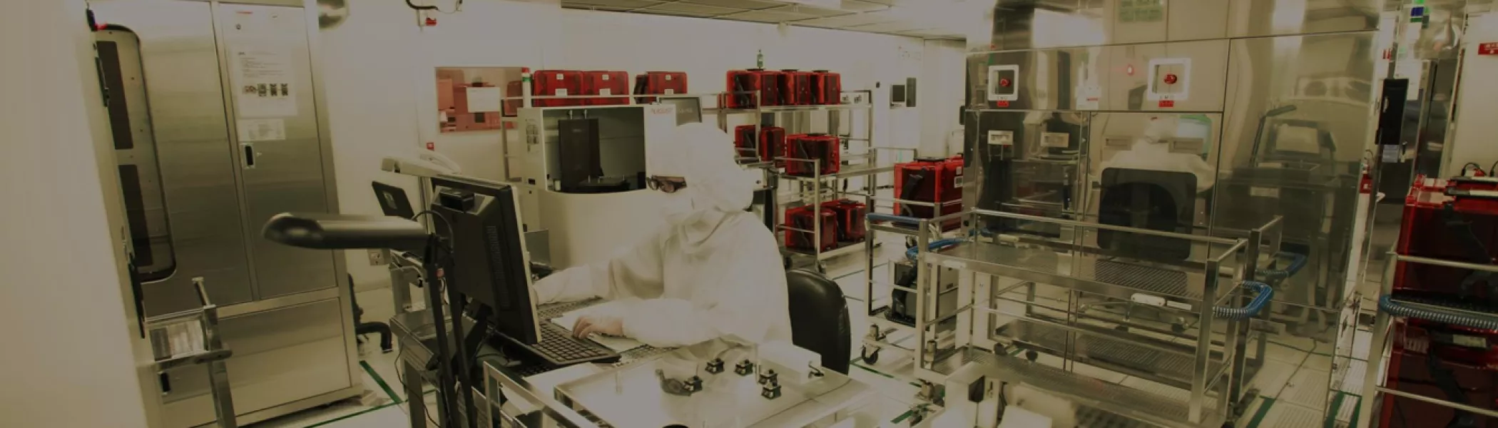
Do you sometimes feel like you are operating in the dark when dealing with the new challenges and opportunities in process and design? These continue to emerge in parallel to ever shrinking semiconductor device geometries.
While Moore’s law and beyond are driving scale reduction, the industry is facing increased process sensitivity and complexity, and is redefining on-wafer defect tolerance in terms of size and complexity.
To detect, identify, understand the source and eliminate yield limiter defectivity are key for total wafer environment contamination characterization and control and are essential for yield enhancement to ensure the success of the latest technology nodes.
It is more imperative than ever that the semiconductor industry works together to enable improved defect detection, speciation/characterization metrology, and as needed, hybrid analytical technology for upcoming HVM readiness.
Join us for this session for speakers and discussion on tackling some of these industry challenges.
Virtual United States
7:30 am
-
7:35 am
Paul Trio
Senior Manager, Strategic Initiatives
SEMI
Welcome
7:35 am
-
7:55 am
Archita Sengupta
Sr. Technologist
Intel
IDM Perspective of Defectivity with regard to Next-Gen Metrology and Analysis Tools
New challenges and opportunities in process and design continue to emerge in parallel to ever shrinking semiconductor device geometries. While Moore’s law and beyond are driving scale reduction, the industry is facing increased process sensitivity and complexity, and is redefining on-wafer defect tolerance in terms of size and complexity.
Join us for this webinar-like session to discuss best-known methods from industry leaders
Challenges in Metrology & Analysis for Next Gen Semiconductor Industry
7:30 am - 10:00 am
Off
Add to Calendar Disabled
America/Los_Angeles
Throwing the Kitchen Sink at IT - Innovations Driving towards a US$1 Trillion Semiconductor Industry
REGISTRATION
Complimentary for SEMI Members.
Use your corporate email address during login to be recognized as a SEMI Member.
The semiconductor industry is expected to reach US$1 trillion by the end of the decade. The next big technology revolutions (AI, 5G/6G, VR/AR, qubit computing, and more) are driving the need to manage exponential amounts of data. Everything from cars to coffee machines are generating data that needs to be moved, stored, computed, secured, and converted to end-user information. To make this a vision a reality requires innovation throughout the semiconductor industry, from new materials to new and improved process equipment to new device architectures designed to perform at speeds and densities once thought unachievable. In this webinar, we will hear from industry experts on what the 10-year technology trends look like and how semiconductor material and equipment suppliers are responding to the trends.
Dr. Todd Younkin, President and CEO of Semiconductor Research Corporation (SRC) will discuss the evolving challenges and five “seismic shifts” that are driving advancement in the semiconductor industry.
Following Dr. Younkin’s talk, David Medeiros, Senior Director, CTO Office of Entegris, Inc. will address these challenges and describe how Entegris is driving materials innovation to overcome the obstacles faced by chip manufacturers.
United States
10:00 am
-
10:03 am
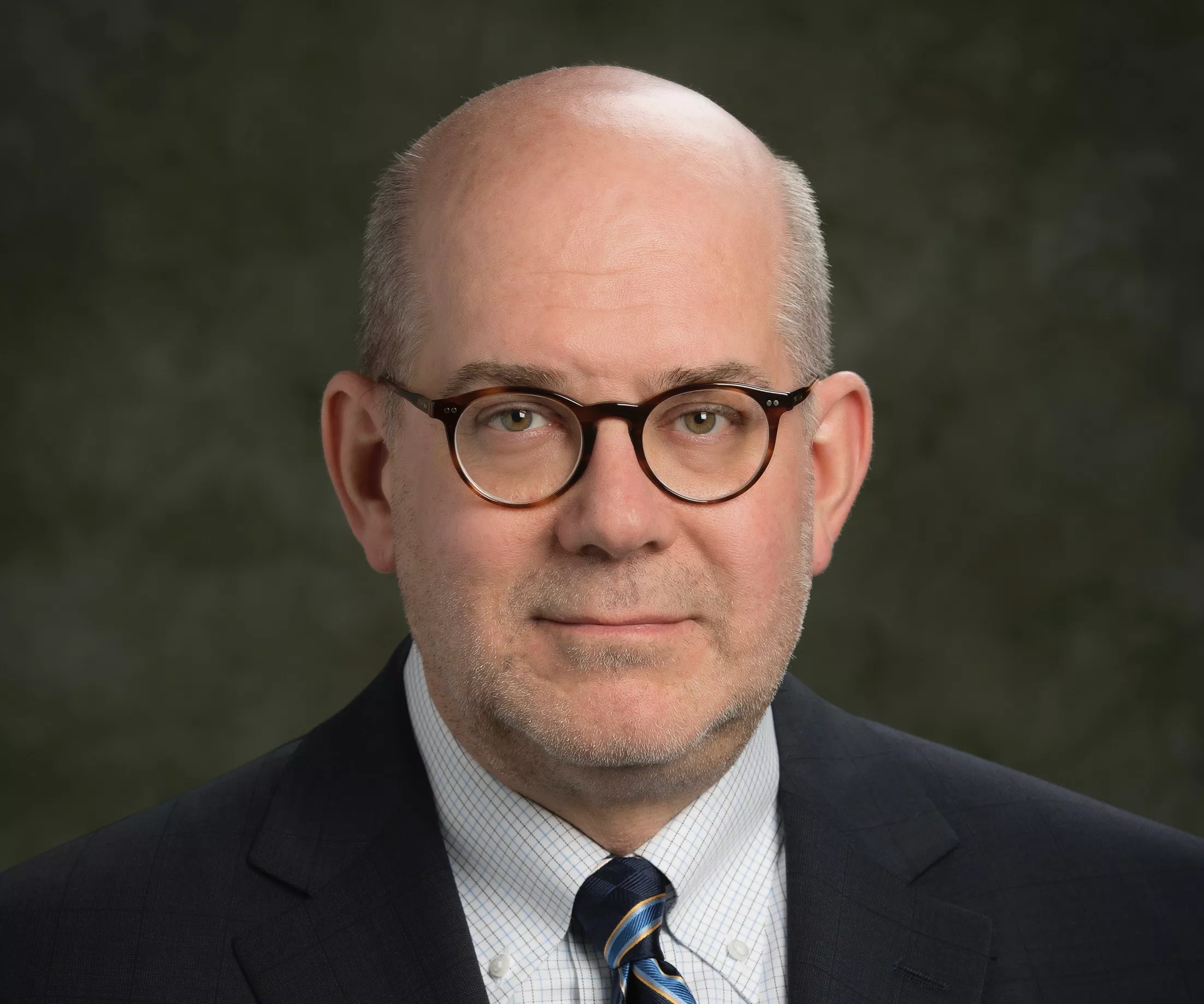
Darron Jurajda
Director, Semiconductor Business Operations
Brewer Science
Session Introduction
Biography: Darron Jurajda is the Director of Semiconductor Business Operations at Brewer Science. He is an expert in materials and process research for anti-reflective materials, multilayer materials, and processes for lithography. He has a diverse background including photolithography, chemical operations, and laboratory research. Darron has published in several technical proceedings and publications including SPIE, IEEE, and Solid State Technology. He has been a member of multiple SEMI Committees over the last 10 years. Darron holds a BS in chemical engineering from the University of Texas at Austin.
10:03 am
-
10:25 am
Todd Younkin
President and CEO
Semiconductor Research Corporation (SRC)
Biography: Dr. Todd Younkin is a talented and seasoned executive with more than 20 years of experience in technology innovation. His extensive Research and Development experience spans Intel’s 0.18um to 5nm nodes with technical contributions in novel materials, nanotechnology, integration, advanced lithography, and integrated photonics. Most recently, he engineered, launched, and led all programmatic aspects of the five-year, $240 million JUMP research initiative. It has six multi-university, multi-disciplinary innovation Centers with 133 faculty, 835 students, and 360 industrial engineering liaisons. It emphasizes the advancement of Computer Science, Electrical Engineering, and Materials to secure continued U.S. thought leadership.
Todd brings a wealth of expertise with strengths in areas such as cultivating relationships with strategic partners, entrepreneurship and investment strategies, technology innovation, operational excellence, and talent management. He has spent much of his career working alongside young minds that are aspiring to influence the ever-changing world of smart and autonomous electronics. He has built programs from the ground up, leveraging his entrepreneurial leadership to drive new business development that has generated multi-millions in funding. He has been a key contributor in introducing new technology advances and starting new global research in the U.S., Europe, and Asia.
Dr. Younkin holds a Ph.D. from the California Institute of Technology in Pasadena, California. He completed his Bachelor of Science at the University of Florida in Gainesville, Florida. He aspires to continue to influence the next generation of technology and inventors, bringing ideas and investors together to drive heterogeneous electronic solutions that will deliver a smarter, shared future.
10:25 am
-
10:45 am
Dave Medeiros
Senior Director, CTO Office
Entegris
Biography: David Medeiros joined Entegris as a Senior Director of Engineering in the office of the CTO in April of 2021. His responsibilities involve developing an enterprise-wide lithography strategy, with a primary focus on the rapidly expanding field of EUV. Previously he spent six years at GLOBALFOUNDRIES (GF), first as the Senior Director of Patterning at Fab 8 in Malta, NY, and later as the Vice President of Central Engineering. Prior to GF, he spent seventeen years at IBM, starting as a Research Staff Member at T. J. Watson Research Center and culminating as the Director of Patterning R&D in the Microelectronics Division. His career began in the semiconductor industry as a synthetic chemist at Shipley Company, which is now part of DuPont. David holds a Ph.D. in Organic Chemistry from the University of Texas, Austin, where he was an Eastman Kodak fellow, and a B.S. in Chemistry from the University of Massachusetts, Amherst.
Innovations Driving towards a US $1 Trillion Semiconductor Industry
Throwing the Kitchen Sink at IT —
10:00 am - 11:00 am
Off
Add to Calendar2021-10-13 10:00:002021-10-13 11:00:00Throwing the Kitchen Sink at IT - Innovations Driving towards a US$1 Trillion Semiconductor IndustryUnited StatesSEMI.org[email protected]America/Los_Angelespublic
MSIG
8:00 am - 9:00 am
Off
Add to Calendar2021-09-29 08:00:002021-09-29 09:00:00Smart City 3D Sensing and Sensor Communications United StatesSEMI.org[email protected]America/Los_Angelespublic
Electromechanical evaluation of printed interconnects
Additive manufacturing of resistors and capacitors
Highly stretchable conductors
Interconnecting in the z direction - printed vias
Printed RF devices and antennas
Device and component placement and assembly
Thinned semiconductor devices
Approaches to bond devices and components to flexible substrates
Concepts of operation and evaluation of performance and reliability
Applications to medical and industrial sensors will be incorporated throughout
About the Instructor
Mark D. Poliks, Ph.D. is a SUNY Distinguished Professor of Engineering and Empire Innovation Professor in Systems Science and Industrial Engineering and Materials Science and Engineering at the State University of New York at Binghamton. He is director of the Center for Advanced Microelectronics Manufacturing (CAMM), a New York State Center of Advanced Technology and home to the New York Node of NextFlex. He serves as Chair of the Smart Energy Transdisciplinary Area of Excellence at the Binghamton campus.
His research is in the areas of industry relevant topics that include high performance electronics packaging, flexible hybrid electronics, medical and industrial sensors, printed RF components, materials, processing, aerosol jet printing, roll-to-roll manufacturing, in-line quality control and reliability of electronics. He is the recipient of the SUNY Chancellor’s Award for Excellence in Research.
He received SEMI FLEXI awards for leadership in Technology and Education in 2009 and 2019. He has authored over one hundred fifty technical papers and holds forty-eight US patents. He was the General Chair of the 69th IEEE ECTC and serves as a IEEE Electronics Packaging Society (EPS) Distinguished Lecturer and an elected member of the IEEE EPS Board of Governors.
This course, the 9th in the FlexTech Master Class Series, takes a deep dive into best known methods for optimizing flexible electronics into medical devices and industrial products. Our expert speaker cover the most important considerations when designing flexible and printable parts and circuits into systems or subsystems and the many approaches to consider.
This course is appropriate for those new to electronics design, as well as those familiar but looking for a refresher on the latest materials and techniques.
Optimizing Design and Fabrication of FHE for Medical and Industrial Applications
ON DEMAND
10:00 am - 12:00 pm
Off
Add to Calendar Disabled
America/Los_Angeles
Session 2: Ultra Wide Band Gap Wafer and Heat Sink Diamond Substrates
4:15 pm - 4:35 pm
Off
Add to Calendar2021-09-23 16:15:002021-09-23 16:35:00Session 1: Ultra Wide Band Gap Wafer and Heat Sink Diamond SubstratesSEMI International Standards Program
Compound Semiconductor Technology Forum
Note: Forum language is mandarin, no simultaneous Interpretation provided
Session 2: Ultra Wide Band Gap Wafer and Heat Sink Diamond Substrates
Speaker: Xing Zhang, CEO of Compound Semiconductor Manufacturing(Xiamen) Co., Ltd
Thursday, September 23, 2021
16:30-17:00
Wuhu, Anhui, China
Webinar Link: Click here
Event Contact information:
Ein Wu
SEMI China
Email: [email protected]
Phone: 86.21.6027.8509ChinaSEMI.org[email protected]America/Los_Angelespublic
Session 2: Progress of VCSEL Technology and Its Applications in 3D Sensing and Lidar
4:35 pm - 5:00 pm
Off
Add to Calendar2021-09-23 16:35:002021-09-23 17:00:00Session 2: Progress of VCSEL Technology and Its Applications in 3D Sensing and LidarSEMI International Standards Program
Compound Semiconductor Technology Forum
Note: Forum language is mandarin, no simultaneous Interpretation provided
Session 2: Progress of VCSEL Technology and Its Applications in 3D Sensing and Lidar
Speaker: Qingwei Mo, Chief scientist of ZJEAGLE.Co., Ltd
Thursday, September 23, 2021
16:35-17:00
Wuhu, Anhui, China
Webinar Link: Click here
Event Contact information:
Ein Wu
SEMI China
Email: [email protected]
Phone: 86.21.6027.8509ChinaSEMI.org[email protected]America/Los_Angelespublic


 Mark D. Poliks, Ph.D. is a SUNY Distinguished Professor of Engineering and Empire Innovation Professor in Systems Science and Industrial Engineering and Materials Science and Engineering at the State University of New York at Binghamton. He is director of the Center for Advanced Microelectronics Manufacturing (CAMM), a New York State Center of Advanced Technology and home to the New York Node of NextFlex. He serves as Chair of the Smart Energy Transdisciplinary Area of Excellence at the Binghamton campus.