Semiconductor technology advancements and added device complexity put ever more stringent requirements on semiconductor manufacturing process monitor and control. Pressure exerted on devices during grinding, CMP, polishing, lamination, bonding, pick and place encapsulation, electrical testing, and packaging can cause failures that may not even be measurable using conventional sensors.
Currently chip test, monitoring and packaging process control is widely done via optical displacement sensors and electrical testing which do not adequately measure the pressure on devices. Without the ability to adequately monitor these processes, root cause failure identification is challenging and maintaining or improving process quality and yield are difficult.
In this webinar the piezoelectric sensor technology will be described and how it used to improve chip test, monitoring and packaging semiconductor processes.
Learn how high-sensitivity, high dynamic range piezo dynamic force measurement sensors can be used to better measure strain during grinding, CMP, polishing, lamination, and electrical test.
MSIG Webinar: Ultra-sensitive, high bandwidth piezoelectric pressure sensors
First in the Innovative Sensors Webinar Series
8:00 am - 9:00 am
Off
Add to Calendar Disabled
America/Los_Angeles
If you are registering to attend the Workshop Virtually, please follow the same registration procedure (via the Button Below) and we will email you the Dial-In information a week before the session.
Registration for this Workshop is separate from SEMICON West registration, but necessary to access the workshop room. To waive the SEMICON West Registration fee, use code "STANDARDSGUEST22" when registering on the SEMICON West Registration page.
In this workshop, our journey of navigating the detection limit obstacle course begins with a broad view of the problem focused on developing a conceptual understanding of key detection limit concepts and limitations. Statistics plays a key role in effective detection limit definition; but need to be the last and final piece of solving the detection limit puzzle where they drive the development of an appropriate statistical practice for detection limit standards.
The current version of SEMI C10 - Guide for Determination of Method Detection Limits sets out important and useful guidance for these concepts. Key detection limit concepts, including the problems caused by our natural biases must be explored and understood. Issues in detection limit and rule-set application will be probed since it is at the application level that detection limit standards succeed or fail.
Workshop Agenda
Part 1: Detecting the Detection Limit – Broad View of Detection Limit Standards / Issues
The Swamp: Why so much disagreement?
Basic Detection Limit concepts
Calibration’s under-appreciated role
Detection Limit Quantification Uncertainty
DL Usage Contexts and Reporting Practices
What’s required to build a Detection Limit standard?
Part 2: SEMI C10 – Guide for Determination of Method Detection Limits
How does it work?
What does it assume?
What are its strengths and limitations?
How should Semi C10 derived Detection Limits be applied?
What form could an update to SEMI C10 take and why?
@ SEMICON WEST Moscone Center San Francisco, CA United States
Join this workshop during SEMICON West 2022 to explore SEMI C10 and discuss how its application to your procedures will improve your yields and manufacturing processes. Quality experts, analytical experts, statisticians and those involved with product quality and process metrics should attend.
Determining the Detection Limit / SEMI C10
A Guide for Determination of Method Detection Limits
10:00 am - 11:30 am
Off
Add to Calendar2022-07-12 10:00:002022-07-12 11:30:00Determining the Detection Limit - SEMI C10Join this workshop during SEMICON West 2022 to explore SEMI C10 and discuss how its application to your procedures will improve your yields and manufacturing processes. Quality experts, analytical experts, statisticians and those involved with product quality and process metrics should attend.@ SEMICON WEST Moscone Center San Francisco, CA United StatesSEMI.org[email protected]America/Los_Angelespublic
America/Los_Angeles
MSIG PNT2 Funding Webinar
Registration for this webinar is free, but required.
This webinar unveiled the details of the 5-year $5M per year ($25M total) Positioning, Navigation, and Timing Phase 2 (PNT2) funded R&D Program starting in 2022. The formal Request for Proposals (RFP) is expected on June 6, 2022.
The PNT2 program follows a successful Phase 1 program that saw 10 projects funded over 2 years starting in 2020 ($6M total funding).
Watch to learn how you can respond to the PNT2 RFP. Topics covered:
technical thrust area
cost share requirements
proposal instructions
team requirements
Q&A
About the Speaker
Dr. Paul Carey joined SEMI in April 2021 and is responsible for managing the MSIG PNT program, the MSIG webinars, and supporting the Manufacturing, Device and Reliability Workgroups and all MSIG related conferences and events. Before joining SEMI, he worked at X-Ray imaging backplane supplier and FOA member, dpiX, in various positions starting in 2003. He was the process, equipment, and yield manager in their Gen 2.5 Palo Alto glass Fab until 2012 when dpiX moved its production to a new Gen 4.5 Fab in Colorado Springs. He rejoined dpiX in 2014 and worked on the flexible substrate equipment selection team and later became their first business development manager in 2018 when dpiX announced its Foundry Business.
Earlier positions were held at Applied Materials where he helped develop a laser annealing system for semiconductor shallow junctions and silicides, and start-up company FlexICs, where he was a co-founder and VP of Engineering. FlexICs developed low temperature thin film transistor (TFT) fabrication technology relevant to flexible OLED displays now used in cellphones. Prior to founding FlexICs, he worked as a staff scientist and program leader at Lawrence Livermore National Laboratory where his group initially developed the low temperature polysilicon-on-plastic TFT technology.
Dr. Carey received a double major BS from UC Berkeley in Electrical Engineering and Computer Science (EECS) and Materials Science and Engineering (MSE). He received his MS in EECS from UC Berkeley and Ph.D. in MSE from Stanford University.
Watch this webinar to learn more about this opportunity to propose for R&D Funding to advance the state-of-the-art in positioning, navigation and timing (PNT) technology.
2022 Focused Solicitation Webinar for PNT2
Positioning, Navigation and Timing Phase 2 Project Funding and Proposal Instructions
8:00 am - 9:00 am
Off
Add to Calendar Disabled
America/Los_Angeles
FlexTech Master Class #12 Additive and Robotics
SEMI Members: $49
Use your corporate email address during log in to be recognized as a SEMI Member.
Non-Members: $99
Students: Free
Contact Gity Samadi ([email protected]) with a picture of your student ID to receive your discount code.
Current electromechanical design practice is predicated on the exercise of expert-level judgement through an interactive and iterative design and fabrication process that requires skilled humans at every step. This approach doesn't scale because it is labor intensive, and therefore biases robots toward longer-lasting, more general-purpose (and expensive) designs in order to justify the development and fabrication costs. Though appropriate in some cases, not all applications are well-served by this process. Many robot applications might be better-served by rapidly-built special-purpose or single-use machines, but automated design and fabrication tools will be critical to control costs, accelerate development, and be responsive to application needs.
The overall goal is to make electromechanical systems (robots) so easy to design and fabricate that we could enable people who are application experts (but not necessarily robot design or fabrication experts) to rapidly create robots for their specific needs. Although Roboticists claim that robots are for dull, dirty, and dangerous use-cases, the community predominantly uses them for the first case, because robots are currently expensive and slow to build, which makes them precious. If we change this situation by making robots practically disposable/expendable, we could potentially re-imagine many robot use-cases.
With this future in mind, new design tools to convert high-level requirements specified by non-experts into concrete electromechanical design plans, new materials that leverage multi-material additive manufacturing, and new multi-material 3D printing methods to automatically convert these designs into functional robots are being developed. During this course we will describe these various areas of current study as well as possible applications for 3D printed robotics.
About the Instructors
Dr. Robert MacCurdy is an assistant professor in Mechanical Engineering at the University of Colorado Boulder where he leads the Matter Assembly Computation Lab (MACLab). He is developing new algorithms, materials, and fabrication tools to automatically design and manufacture electromechanical systems, with a focus on robotics. Rob did his PhD work with Hod Lipson at Cornell University and his postdoctoral work at MIT with Daniela Rus. He holds a B.A. in Physics from Ithaca College, a B.S. in Electrical Engineering from Cornell University, and an M.S. and PhD in Mechanical Engineering from Cornell University.
Dr Gregory Whiting is an Associate Professor in the Department of Mechanical Engineering and a member of the Materials Science and Engineering Program at the University of Colorado Boulder (CU). At CU he leads the Boulder Experimental Electronics and Manufacturing (BEEM) Laboratory, which is focused on studying and developing materials, processes and devices for novel and additively manufactured electronic systems used in applications including distributed sensing (particularly for environmental monitoring) and robotics. Prior to joining CU in 2017, Greg was a member of the Rapid Evaluation Team at Google[X] and managed the Novel Electronics Area at the Palo Alto Research Center. He received a PhD from Cambridge University in 2007 and a BS from UC Berkeley in 2002.
Fabricating robots using additive design and manufacturing methods has the potential to transform when, where and how the advantages of robots are brought to bear.
Take this FlexTech Master Class to explore the potential applications and how to use new design tools, 3D printing methods and multi-material additive manufacturing to convert ideas into solid electromechanical robotic systems.
Led by Dr. Robert MacCurdy and Prof. Greg Whiting of the University of Colorado, Boulder, this course will provide you new ways to approach manufacturing, additive design and the role of robots.
A New Approach to Robotics: Designing for Additive Manufacturing
Flexible Hybrid and Printed Electronics Master Class
10:00 am - 12:00 pm
Off
Add to Calendar Disabled
America/Los_Angeles
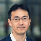
Dr. Chris Huang currently serves as Deputy Project Manager for MEMS & Photonics Engineering at ASE. In his current role, he is focused on MEMS and optical sensor packaging in automotive applications, as well as smart sensor and smart system technologies for emerging applications. Since joining ASE over four years ago, he has gained significant experience in the fields of sensor and actuator design, MEMS device and wafer manufacturing, and sensor packaging, including extensive work in the field of microfabrication of piezoresistive MEMS sensors and wafer bonding process.
Prior to ASE, he worked as an R&D Technologist at Asia Pacific Microsystems Inc., a pure-play MEMS foundry, where he managed the development of standard fabrication platforms for customizable sensors, such as MEMS optical actuators/piezoresistive pressure and force sensors. Dr. Huang has published over thirty-five technical SCI journal papers and international conference papers and holds eight worldwide patents on MEMS and sensor applications. Dr. Huang received his Ph.D. from National Tsing Hua University, Taiwan, where he also completed work as a post-doctoral researcher within the Department of Power Mechanical Engineering
The incredible power of MEMS technology and sensor applications has been elevated onto the world stage in recent times, given how they help enable technology and applications that are literally changing lives, from health to transportation, from robotics to AI, from edge to cloud, and from 5G to beyond.
During this SEMI MSIG webinar, ASE’s Dr. Chris Huang will elaborate and put a spotlight on the role that packaging technologies play and the innovation evolving to progress miniaturization and integration, both key attributes within the MEMS and Sensors arena.
He will present unique approaches required to overcome MEMS and Sensor packaging and test challenges and achieve highest possible performance when responding and interacting with any external or environmental stimuli.
Q&A will follow.
MSIG Webinar: MEMS & Sensors Packaging for Limitless Applications
Third in the Foundry, Dicing & Packaging Series
8:00 am - 9:00 am
Off
Add to Calendar Disabled
America/Los_Angeles
Mahesh Chowdhary, Ph.D. is a Fellow and Director of Strategic Platforms & IoT Excellence Center at STMicroelectronics based in Santa Clara CA. He leads effort on development of solutions and reference designs for mobile phones, consumer electronic devices, automotive and industrial applications that utilize MEMS sensors, computing and connectivity products. His area of expertise includes AI/ML, MEMS sensors, IoT, digital transformation, and location technologies. He has been awarded 30 patents. He has spoken extensively internationally about Machine Learning, Smart Sensors, and IoT. Mahesh received PhD in Applied Science (Particle Accelerators) from the College of William & Mary in Virginia. He is also an Adjunct Professor at IIT, Delhi.
Mahaveer Jain - Mahaveer Jain is Application Principal Engineer at STMicroelectronics(Santa Clara, CA) and specializing in MEMS sensors, Algorithm, DSP, and Machine Learning . Over the course of his career, Mahaveer worked on indoor navigation, hybrid positioning , sensor calibration, and sensor fusion. His most recent work has been developing extremely low power machine learning models to run on sensors. Mahaveer received a Bachelor of Technology in Physics from IIT Delhi.
Denis Ciocca - Denis is Staff Applications Engineer at STMicroelectronics specializing in Linux OS, Linux device drivers, Android OS, and Smart sensors. He has developed a variety of solutions with MEMS sensors, a computational platform of STM32 microcontrollers and wireless connectivity solutions. Denis has received his Master’s degree in Computer Science and Engineering from the University of Pavia, Italy.
This class will explain and demonstrate how AI/ML logic can be implemented on Edge devices such as Smart sensors. Power efficiency, latency, and bandwidth considerations are important for AI/ML implementation on Edge devices. Computing can be distributed between Edge devices and Cloud. The latest trends and applications of smart sensors in consumer electronics, automotive, and industrial use cases will be discussed.
Course Outline:
AI / ML on Edge devices
Why AI / ML on Edge devices?
Power efficiency, latency and bandwidth considerations when executing AI / ML logic on Edge devices.
Computing distribution between Edge device, gateway and Cloud.
Assignment: Finite State Machine and Decision Tree applications
Introduction to Inertial Sensors with AI / ML capabilities
Background on inertial sensors including applications
Typical performance characteristics of inertial sensors
Lab: SensorTile.Box and use of custom sensors to change sensor sampling rate, filters, and other configuration.
Machine Learning Core (MLC) in Smart Sensor
An introduction ML at Edge of the Edge, Smart Sensors: Latest trends Applications of Smart sensors applications in consume electronics, automotive, industrial use cases. Next generation of smart sensors.
AI on the Edge and requirements of distributed intelligence system.
Introduction to MLC framework
Input data
Filters and Feature selection
Optimization
Tools
Rapid Prototyping with MLC: current consumption under 10 uA
Lab: Motion Intensity detection using MLC. Lab conducted using AlgoBuilder tool.
Finite State Machines (FSM) in Smart Sensor
Introduction to FSM
Input data
FSM definition and structure
Conditions list
Tools
Rapid Prototyping using FSM:
Lab: Gesture recognition using FSM. Lab conducted using AlgoBuilder Tool.
SEMI 673 South Milpitas Avenue Milpitas, CA95035 United States
Mahesh Chowdhary, Ph.D.
Fellow & Director of Strategic Platforms & IoT Excellence Center
Earn CEUs and IEEE PDHs from this hands-on SEMI MSIG Master Class & Lab, where instructors will explain and demonstrate how AI/ML logic can be implemented on edge devices such as smart sensors. Attendees will build and operate their own edge device with AlgoBuilder tools in 2 lab sections of the course.
This course is designed for applications engineers wanting to learn how to add sensors to an existing or new product. Instructors are experienced STMicroelectronics engineers with many sensor design and implementations.
The course covers many topics including the importance of power efficiency, latency, and bandwidth considerations for AI/ML implementation on edge devices. Learn how computing can be distributed between the edge devices and the cloud. The latest trends and applications of smart sensors in consumer electronics, automotive, and industrial use cases will also be discussed.
Join us in person at SEMI HQ, for this hands-on learning experience.
This course is underwritten by STMicroelectronics.
Ai/ML on Edge Devices and Smart Sensor Integration Master Class
8:30 am - 5:30 pm
Off
Add to Calendar Disabled
America/Los_Angeles
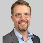
About the Speaker: Rich Boardman is a 15-year veteran of the Semiconductor industry whose expertise lies in equipment sets, process technology and consumables related to wafer or substrate dicing, grinding or polishing. Rich is a Senior Sales Engineer at GDSI, located in San Jose, California.
United States
Richard Boardman
Senior Sales Engineer
GDSI
Join us for this second webinar in the MSIG series on foundries, dicing, and packaging considerations in MEMS fabrication.
In this session, GDSI will provide an introduction of the Stealth Dicing process, highlight the applications it is most well suited to, and share design rules and process window specifications.
The Stealth laser dicing process is a water-free, particle-free wafer singulation method. It is particularly well suited to MEMS, Quantum, bio-sensing and Silicon Photonics to name a few use cases. Secondarily, it offers great value for multi-project wafer (MPW) applications since it allows singulation of the whole wafer in a single process step, negating the need for wafer sub-dicing and remounting.
Find out if your current wafer layout is compatible with the Stealth Dicing process, and if not, what must be done to ensure initial success with this innovative dicing technology. .
MSIG Webinar: The New GDSI Dicing Process
March 30, 2002 8-9 AM PT
8:00 am - 9:00 am
Off
Add to Calendar2022-03-30 08:00:002022-03-30 09:00:00MSIG Webinar GDSI Dicing ProcessJoin us for this second webinar in the MSIG series on foundries, dicing, and packaging considerations in MEMS fabrication.
In this session, GDSI will provide an introduction of the Stealth Dicing process, highlight the applications it is most well suited to, and share design rules and process window specifications.
The Stealth laser dicing process is a water-free, particle-free wafer singulation method. It is particularly well suited to MEMS, Quantum, bio-sensing and Silicon Photonics to name a few use cases. Secondarily, it offers great value for multi-project wafer (MPW) applications since it allows singulation of the whole wafer in a single process step, negating the need for wafer sub-dicing and remounting.
Find out if your current wafer layout is compatible with the Stealth Dicing process, and if not, what must be done to ensure initial success with this innovative dicing technology. .United StatesSEMI.org[email protected]America/Los_Angelespublic
America/Los_Angeles
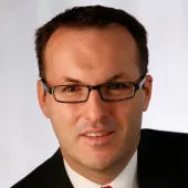
About the Speaker: Robert MacDonald is a MEMS engineer at GE’s Research. His research is focused on high performance inertial sensors. He has over 20 years of experience in the MEMS and semiconductor industries. His work has covered the product life cycle of chemical, inertial and optical sensors from design through market introduction and manufacturing.
Join us for this first webinar in the MSIG series on foundries, dicing, and packaging considerations in MEMS fabrication.
In this first in the series, GE Research will present their new MEMS process suitable for bulk silicon motion sensors. The process aims to deliver many features of complex MEMS flows, such as wafer level packaging with through silicon vias (TSVs), with a short cycle times and low mask counts. This webinar will introduce the Polaris process within the GE Research foundry and explain how to design the process, and our model for delivering new designs.
Designing MEMS with GE’s Polaris Process for Motion Sensor Fabrication
8:00 am - 9:00 am
Off
Add to Calendar2022-03-02 08:00:002022-03-02 09:00:00MSIG Webinar GE Polaris ProcessJoin us for this first webinar in the MSIG series on foundries, dicing, and packaging considerations in MEMS fabrication.
In this first in the series, GE Research will present their new MEMS process suitable for bulk silicon motion sensors. The process aims to deliver many features of complex MEMS flows, such as wafer level packaging with through silicon vias (TSVs), with a short cycle times and low mask counts. This webinar will introduce the Polaris process within the GE Research foundry and explain how to design the process, and our model for delivering new designs.United StatesSEMI.org[email protected]America/Los_Angelespublic
America/Los_Angeles
Moore’s Law continues to evolve - dramatically changing the Field Effect Transistor (FET). As FinFETs reach their performance limits, attention is turning to Gate All Around (GAA) architectures based on Horizontal Nanosheet technology. Such a fundamental shift in transistor architecture will create new challenges to processes and materials, presenting opportunities for companies well-positioned for this shift.
In this webinar, SEMI EMG brings experts to explain the technology trends driving the industry adoption of Gate All Around, how the major players are approaching this transition, and the implications this will have on the material supply chain
Gate All Around Transistors - Opportunities Abound
Position yourself for the next chapter of Moore's Law
10:00 am - 11:00 am
Off
Add to Calendar Disabled
America/Los_Angeles
Dr. Toni Mattila is the Head of Sustainable Manufacturing at Business Finland, which is a governmental agency for R&D and innovation funding, business development and internationalization services. Toni leads a national business development program with the goal of transforming Finnish manufacturing industries towards sustainable development. Toni worked for fourteen years in academia as a researcher in the field of microelectronics. Toni is an active member of IEEE Electronics Packaging Society, and a frequent attendee of various electronics conferences.
This Master Class was held live on December 1, 2021. It is still available On Demand.
Sustainability is more a way of thinking than a technological solution. To achieve sustainability, a company must develop a comprehensive approach that covers multiple levels and segments of its business.
Watch this course to develop an understanding of the essential components of industrial carbon footprint and discuss actions companies and industry can take to reduce theirs. Throughout the course, we paid particular attention to the electronics industry; what the sector has already contributed and what remains to be achieved.
The role of new technologies – e.g. FHE - was discussed and what role they play in reducing the carbon footprint so that ‘sustainability’ can become a sustainable business.
Watch this course to focus on a broader picture of sustainability in the electronics sector.
Environmental Sustainability and Flexible & Printed Electronics
9:00 am - 11:00 am
Off
Add to Calendar Disabled
America/Los_Angeles


 Dr. Chris Huang currently serves as Deputy Project Manager for MEMS & Photonics Engineering at ASE. In his current role, he is focused on MEMS and optical sensor packaging in automotive applications, as well as smart sensor and smart system technologies for emerging applications. Since joining ASE over four years ago, he has gained significant experience in the fields of sensor and actuator design, MEMS device and wafer manufacturing, and sensor packaging, including extensive work in the field of microfabrication of piezoresistive MEMS sensors and wafer bonding process.