EMG
Off
Add to Calendar2021-12-23 00:00:002021-12-23 00:00:00SEMI China Material Committee 3rd MeetingShanghai ChinaSEMI.org[email protected]America/Los_Angelespublic
Silicon on Insulator technology is a very diverse and multi-faceted enabler of semiconductor products. In certain areas if offers performance advantages across a wide dynamic range of leakage and in other areas it enables the use of high voltages in multi-domain designs. It also inherently bring low capacitance which makes it great for ultra-fast switching in RF designs and significantly improved radiation robustness compared to bulk CMOS; it’s easy to see why SOI technology continues to expand in use through-out the industry.
Attend this webinar to see how these advantages are being applied to products in the medical and automotive (and more) application spaces.
CA United States
8:00 am
-
8:10 am
Carlos Mazure
SOI Consortium
Welcome and Introduction
8:10 am
-
8:30 am
Jon Cheek
Sr. Director, Process Technology Development
NXP Semiconductor
SOI Technology: Enabling Everything from Automotive to 6G
Abstract – The use of Fully-Depleted SOI, FD-SOI, combined with an ultrathin buried oxide create a technology ideally suited for the Internet of Things revolution. FDSOI enables the dynamic modulation of the threshold voltage during operation, not just during the design phase, to open a whole new world of creative product opportunities. One such example is the creation of ultralow leakage embedded SRAM memories which consume so little power that some resulting IoT products can last years on a single household battery. Other versions of SOI Technology with thick buried oxide enable use of 50V to 70V domains on a chip without need of complex isolation schemes. This ability to provide high voltage support along with digital processing is yet another reason SOI is adopted to provided differentiation in product offerings. Each of these approaches will be discussed and shown how it benefits the final products.
8:30 am
-
8:50 am
Giulio Ricotti
Design Director & Technical Staff Fellow
ST Microelectronics
BCBD-SOI Technologies and Applications in Ultrasound Imaging and More
Giulio Ricotti – Design Director and Technical Staff Company Fellow - STMicroelectronics
After earning his Electronics Engineering degree, Giulio joined ST in 1994 as a design engineer in their Smart Power (SP) products group. Currently a Design Director and Technical Staff Company Fellow, Giulio has more than 60 patents and has authored 70 publications. Giulio has also been awarded the “Premio dei Premi” in 2009 by the Italian president Giorgio Napolitano for his crucial contribution to innovation with the 4D ultrasound imaging project that is used today all over the world for pregnancy and cardiology screenings.
Join us for the the first in a series of webinars focused on applications of SOI technology, brought to you by the SEMI SOI Consortium. The series will underline the breadth of products that SOI technologies cover.
The first webinar of the series will feature ST Microelectronics and NXP. ST Microelectronics will focus on their BCD-SOI technologies and applications, such as medical ultrasound imaging. NXP will showcase multiple applications of SOI technologies in automotive from power electronics through infotainment.
Latest Trends in SOI-based Microelectronics Applications
8:00 am - 9:00 am
Off
Add to Calendar Disabled
America/Los_Angeles
Dr. Toni Mattila is the Head of Sustainable Manufacturing at Business Finland, which is a governmental agency for R&D and innovation funding, business development and internationalization services. Toni leads a national business development program with the goal of transforming Finnish manufacturing industries towards sustainable development. Toni worked for fourteen years in academia as a researcher in the field of microelectronics. Toni is an active member of IEEE Electronics Packaging Society, and a frequent attendee of various electronics conferences.
This Master Class was held live on December 1, 2021. It is still available On Demand.
Sustainability is more a way of thinking than a technological solution. To achieve sustainability, a company must develop a comprehensive approach that covers multiple levels and segments of its business.
Watch this course to develop an understanding of the essential components of industrial carbon footprint and discuss actions companies and industry can take to reduce theirs. Throughout the course, we paid particular attention to the electronics industry; what the sector has already contributed and what remains to be achieved.
The role of new technologies – e.g. FHE - was discussed and what role they play in reducing the carbon footprint so that ‘sustainability’ can become a sustainable business.
Watch this course to focus on a broader picture of sustainability in the electronics sector.
Environmental Sustainability and Flexible & Printed Electronics
9:00 am - 11:00 am
Off
Add to Calendar Disabled
America/Los_Angeles
Off
Add to Calendar2021-10-27 00:00:002021-10-27 00:00:00Joint SEMI-CAR virtual event: Chip Shortage Impact on AutomotiveVirtual, Eastern Time United StatesSEMI.org[email protected]America/Los_Angelespublic
9:00 am - 5:30 pm
Off
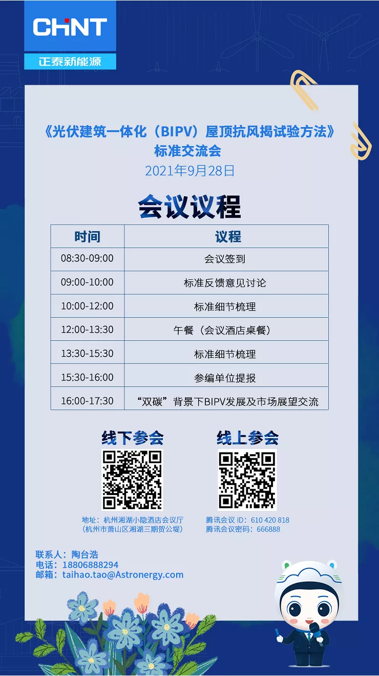
Add to Calendar2021-09-28 09:00:002021-09-28 17:30:00BIPV TASK FORCE MEETINGBIPV TASK FORCE MEETING
光伏建筑一体化(BIPV)屋顶抗风揭试验方法标准交流会ChinaSEMI.org[email protected]America/Los_Angelespublic
10:00 am - 11:30 am
Off
Add to Calendar2021-09-17 10:00:002021-09-17 11:30:004H-SiC Homoepitaxial Wafer Task Force Meeting 会议邀请:4H-SiC同质外延片工作组线上会议
4H-SiC Homoepitaxial Wafer Task Force Meeting
Meeting:Link
Friday, September 17, 2021
10:00-11:30ChinaSEMI.org[email protected]America/Los_Angelespublic
Do you sometimes feel like you are operating in the dark when dealing with the new challenges and opportunities in process and design? These continue to emerge in parallel to ever shrinking semiconductor device geometries.
While Moore’s law and beyond are driving scale reduction, the industry is facing increased process sensitivity and complexity, and is redefining on-wafer defect tolerance in terms of size and complexity.
To detect, identify, understand the source and eliminate yield limiter defectivity are key for total wafer environment contamination characterization and control and are essential for yield enhancement to ensure the success of the latest technology nodes.
It is more imperative than ever that the semiconductor industry works together to enable improved defect detection, speciation/characterization metrology, and as needed, hybrid analytical technology for upcoming HVM readiness.
Join us for this session for speakers and discussion on tackling some of these industry challenges.
Virtual United States
7:30 am
-
7:35 am
Paul Trio
Senior Manager, Strategic Initiatives
SEMI
Welcome
7:35 am
-
7:55 am
Archita Sengupta
Sr. Technologist
Intel
IDM Perspective of Defectivity with regard to Next-Gen Metrology and Analysis Tools
New challenges and opportunities in process and design continue to emerge in parallel to ever shrinking semiconductor device geometries. While Moore’s law and beyond are driving scale reduction, the industry is facing increased process sensitivity and complexity, and is redefining on-wafer defect tolerance in terms of size and complexity.
Join us for this webinar-like session to discuss best-known methods from industry leaders
Challenges in Metrology & Analysis for Next Gen Semiconductor Industry
7:30 am - 10:00 am
Off
Add to Calendar Disabled
America/Los_Angeles