downloadGroupGroupnoun_press release_995423_000000 copyGroupnoun_Feed_96767_000000Group 19noun_pictures_1817522_000000Member company iconResource item iconStore item iconGroup 19Group 19noun_Photo_2085192_000000 Copynoun_presentation_2096081_000000Group 19Group Copy 7noun_webinar_692730_000000Path
Skip to main content
Default Banner Image

Vietnam

China India Japan Malaysia Singapore South Korea Taiwan Vietnam Understanding Semiconductor Technology and Business (Asia) Training

Course Description

The first part of the course provides a brief overview of semiconductor design and fabrication steps, encompassing IC design techniques, all wafer processing steps, assembly, and packaging. It delves into semiconductor jargon in laypeople terms, and various substrate types such as Si, SiGe, FDSOI, GaAs, SiC, GaN. Additionally, it discusses different types of transistors like pMOS, nMOS, Bipolar, BiCMOS, CMOS, FinFets, and GAA and their evolution and what applications they are used in.
 
The second part of the course focuses on semiconductor business aspects such as silicon economics, wafer processing costs, semiconductor revenue forecasts, driving forces in the industry, top semiconductor IDMs, market competitors based on market share, OEMs, foundries, top tool vendors, and Fabless companies.  Addresses the fastest-growing semiconductor markets based on geographic locations and applications, identifies semiconductor competitors/customers, and discusses major semiconductor markets like Automotive, PC, Mobile, Memory, Wireless, Cell phones, Consumer, Gaming, AI, IoT, Digital TV, Radio, Automotive, MEMS, and Emerging Technology & Impact on Industry.

Learning Objectives

  • Understand the fundamental principles and theories semiconductor technology.
  • Communicate with other associates and understand wafer processing steps.
  • Understand semiconductor business aspects such as silicon economics, wafer processing costs, semiconductor revenue forecasts, driving forces in the industry, top semiconductor IDMs, market competitors based on market share, OEMs, foundries, top tool vendors, and Fabless companies.
  • Review the semiconductor eco-system as it relates to design and fabrication of a semiconductor device.
  • Gain knowledge of major semiconductor markets like Automotive, PC, Mobile, Memory, Wireless, Cell phones, Consumer, Gaming, AI, IoT, Automotive, MEMS, and Emerging Technology & Impact on Industry.
  • Demonstrate effective communication skills through written reports, presentations, and discussions related to semiconductor subjects.
  • Collaborate effectively with peers in group projects or discussions regarding semiconductor subjects.
  • Analyze and evaluate research literature in semiconductor technology.
  • Develop critical thinking and problem-solving skills applicable to semiconductor technology.

Who Should Attend

This course is suitable for anyone seeking a better understanding of the semiconductor industry, market leaders, terminology, business, and the semiconductor ecosystem.

Instructor

Denny Frye 

PT International, LLC

Instructor Bio
 

Important Information

Note that only the person who registered will receive a certificate of completion. This virtual training will not be recorded. Attendees must be present to access course knowledge. 

Can't find the training link day of? After you register, you will receive the link to the live training via the email address you provided. In addition, you will receive email reminders about 24 hours in an advance and an hour before with the same link. Please keep these emails on hand to access the trainings on time. If you do not see any confirmation emails, please check your junk/spam folders before contacting SEMI U for support. 

Singapore

SEMI U

Embark on a journey through semiconductor design, manufacturing, and business in this illuminating course. Explore IC design techniques, transistor evolution, and market dynamics. Delve into substrate types and industry economics, discovering the fastest-growing markets and key players shaping the semiconductor landscape.

Pricing
  • Members: $745
  • Non-Members: $845

* For group orders with 10+ attendees, and for Students/Veterans discounted pricing, please contact [email protected].

9:00 am - 4:30 pm Off Add to Calendar 2025-07-16 09:00:00 2025-07-16 16:30:00 Understanding Semiconductor Technology and Business (Virtual Training, Asia) Embark on a journey through semiconductor design, manufacturing, and business in this illuminating course. Explore IC design techniques, transistor evolution, and market dynamics. Delve into substrate types and industry economics, discovering the fastest-growing markets and key players shaping the semiconductor landscape.PricingMembers: $745Non-Members: $845* For group orders with 10+ attendees, and for Students/Veterans discounted pricing, please contact [email protected]. Singapore SEMI.org [email protected] Asia/Singapore public Asia/Singapore Sold Out
Event format
Promote in calendar
Off

From January 1, 2025 Heraeus is combining the high-performance materials expertise of Heraeus Conamic and Heraeus Comvance into a new operating company: Heraeus Covantics. The merged business will be led by a new management team. The legal entities will remain the same.

With the new operating company, Heraeus is further expanding its technology leadership in the manufacturing and processing of high-purity quartz, fused silica, and other high-end materials such as ceramics and innovative composites.

“We are creating a global powerhouse in which we drive innovation and exploit technological synergies,” explain Christoph Fark, Michael Werth and Nikolas Pojezny, Managing Directors of Heraeus Covantics. ”The new structure more closely aligns our combined capabilities and competencies with market requirements and customer needs. This enables our customers to strengthen their competitive advantage.”

Heraeus Covantics manufactures semi-finished products, complex system components and custom-tailored solutions made of quartz glass, fused silica and ceramic materials. They are used in the data transmission and telecommunication industry, the production of specialty optical fibers for industrial and medical applications, semiconductor manufacturing and optical applications among others.

About Heraeus
Heraeus is a family-owned global technology group headquartered in Hanau, Germany. The company’s roots go back to a family pharmacy started in 1660. With its expertise and resources, Heraeus has been making meaningful contributions over generations and is committed to do so in the future. Today, the group bundles diverse activities in four Business Platforms: Metals and Recycling, Healthcare, Semiconductor and Electronics, as well as Industrials. Customers benefit from innovative technologies and solutions based on broad materials knowledge and technological leadership. In the 2023 financial year, the group generated revenues of €25.6 billion (US$27.7 billion*) with approximately 16,400 employees in 40 countries. Heraeus is one of the top 10 family-owned companies in Germany.

About Heraeus Covantics
Heraeus Covantics is a technology leader specializing in the manufacturing and processing of the industry’s highest purity quartz, fused silica and other high-end materials such as ceramics and composites. With locations in Europe, USA and Asia, Heraeus Covantics manufactures semi-finished products, complex system components and custom-tailored solutions made of quartz glass, fused silica and ceramic materials. They are used in the data transmission and telecommunication industry, the production of specialty optical fibers for industrial and medical applications, semiconductor manufacturing and optical applications among others.

Innexis delivers a set of products and capabilities to address demand for shift-left software development in the IC development process

With more demanding software workloads, it is critical to facilitate the development and execution of realistic workloads early in the design phase to shorten overall development time and identify hardware and software defects earlier
Siemens Digital Industries Software announced today the Innexis product suite, a complement to its industry leading Veloce™ hardware-assisted verification and validation system.

Building on the success and rapid adoption of Veloce, Siemens’ Innexis product suite delivers a set of capabilities to address customer demand for shift-left software in the early phases of IC development. These products include a hardware/software development flow from virtual to hybrid to full RTL, an architecture native virtual platform for early high-speed software development and a simulation backplane that enables the development of digital twins in Siemens’ PAVE360™ software for software-defined vehicles and other complex systems.

“The complexity of integrated circuits (IC) is increasing exponentially, designers need more efficient methodologies to meet industry demands. Veloce has seen rapid adoption by industry leaders to help solve this critical bottleneck. The Innexis product suite extends workflow improvements from Veloce to help our customers shift left their IC development and debug cycle,” said Jean-Marie Brunet, vice president and general manager, Hardware-Assisted Verification, Siemens Digital Industries Software. “This enables IC design to begin months before final RTL, all while using a common software workload across the development process.”

Adoption of a shift-left approach for software development and IP verification processes is now mandatory. As chip designs become increasingly complex due to more demanding software workloads, it is critical to enable the development and execution of realistic workloads early in the design phase. A proactive shift-left software approach helps mitigate the risk of identifying issues late in the development cycle.

“The implementation of Innexis in our development process has significantly enhanced software and system validation performance, thereby improving the efficiency of our teams and projects. By enabling heterogeneous component modeling within virtual platforms, it allows us to create realistic high-speed models of System on Chips (SoCs),” said Ari Hautala, Principal System Architect, Nokia Mobile Networks. “Furthermore, the integration of these high-speed virtual platforms with RTL IP on Veloce emulators facilitates superior overall performance while still permitting precise cycle-accurate performance and power analysis on RTL model components. Additionally, Innexis offers exceptional visibility and debuggability for the SoC design, along with the capability to integrate and execute a large number of complex test cases effectively.”

Currently, the Innexis product suite consists of:

Innexis Developer Pro: Innexis Developer Pro software provides a connected development flow from virtual to hybrid to full RTL. This provides a comprehensive environment for accelerating the creation of complex SoC design supporting a wide range of use-cases including seamless hardware-software co-development, co-validation, and pre-silicon cycle accurate analysis and validation. Innexis Developer Pro supports the modelling of complex SoC’s with heterogeneous cores and custom SystemC model components. In addition, it provides the ability to run in both virtual plus RTL hybrid mode for high performance execution, and then at a time of interest switch to full RTL emulation enabling high accuracy analysis of the full SoC when required.

Innexis Architecture Native Acceleration (ANA): Innexis Architecture Native Acceleration software is a cloud- based high-speed virtual platform. By running natively on Arm based servers the software workloads run at much higher speeds than on typical instruction set simulation based virtual platforms. Cloud hosting also provides scalable compute resources and simple browser-based access and tools. Innexis Architecture Native Acceleration can also run on local Arm based servers if preferred. In both cases it enables early software development and testing, and early software defect identification.

Innexis Virtual System Interconnect: Innexis Virtual System Interconnect software facilitates the creation and simulation of comprehensive system level digital twin platforms by seamlessly connecting multi-behavioral virtual and physical subsystems, supporting a variety of communication protocols. Innexis Virtual System Interconnect behavioral models can include Innexis Developer Pro or Innexis Architecture Native Acceleration SoC models, supporting system-level shift-left software development and RTL verification.

To learn more about Siemens’ Innexis product suite and how it addresses the demand for shift-left software development in the integrated circuit development process, visit: www.siemens.com/innexis

About Siemens
Siemens Digital Industries Software helps organizations of all sizes digitally transform using software, hardware and services from the Siemens Xcelerator business platform. Siemens' software and the comprehensive digital twin enable companies to optimize their design, engineering and manufacturing processes to turn today's ideas into the sustainable products of the future. From chips to entire systems, from product to process, across all industries. Siemens Digital Industries Software – Accelerating transformation.

Note: A list of relevant Siemens trademarks can be found here. Other trademarks belong to their respective owners.

Heidelberg Instruments Reports Major Orders for the VPG+ 1400 FPD Volume Pattern Generator from Leading Asian Photomask Manufacturers

Heidelberg, Germany – Heidelberg Instruments has secured two major orders for its VPG+ 1400 FPD Volume Pattern Generator from leading photomask manufacturers in Asia, with a total order value between EUR 9 million and EUR 10 million. Deliveries are scheduled for 2025.

“These significant order intakes mark major milestones for the company, reinforcing our market position and driving further innovation and growth in the display technology sector”, says Alexander Forozan, VP of Global Sales and Business Development.

The VPG+ 1400 is Heidelberg Instruments’ largest system, specifically designed for large-format photomask patterning in the flat panel display (FPD) industry. It supports mask sizes up to 1400 x 1400 mm², making it ideal for various flat panel display generations (G4 to G8). The VPG+ 1400 sets a new standard for high-throughput photomask production, offering the precision and scalability required for large displays. Additionally, it delivers the accuracy needed to produce large-area halftone photomasks for flat panel displays.

Equipped with advanced metrology and alignment features, including Cognex AI-based image recognition, the system ensures precise alignment for multilayered masks. Its linear and nonlinear coordinate corrections further enable precise overlay across tools.
By addressing the diverse exposure needs of customers, Heidelberg Instruments' large-area VPG+ Volume Pattern Generators have proven to be valuable assets in display photomask production lines.

Further information: https://heidelberg-instruments.com/product/vpg-1400-fpd/

Malaysia Singapore Vietnam SEMI x MSIA Members' Networking Night EventTile Business Executive
Highlighted content

Hotel Rates

G Hotel Gurney

Room Type

Size (m²)

Room Only

Room + Breakfast (Single)

Room + Breakfast (Double)

Deluxe

38

550

580

610

Executive Rooms & Suites

Executive Room

38


710

710

Duplex Suite

88


780

780

L Suite

67


900

900

Executive Suite

78


1,050

1,050

XL Suite (2 Bedrooms)

113


1,550

1,550

G Suite

187


2,420

2,420


All rates are in MYR.

Guests wishing to book a room at G Hotel Gurney are required to contact the hotel representative, Pei Leng, at +60 17-466 8032 or via email at [email protected].


Eastern & Oriental Hotel | SOLD OUT

Victory Annexe Wing

Studio Suite

580++

Corner Suite

1,580++

Heritage Wing

Deluxe Suite | Georgetown Suite | Superior Suite

780++

Premier Suite

850++

Straits Suite

1,130++

Writer Suite

2,080++

Pinang Suite

2,980++


All rates are in MYR.

All Eastern & Oriental Hotel rates include breakfast for two. (Single occupancy rates are not available.)

Guests wishing to book a room at Eastern & Oriental Hotel are required to contact the hotel representative, Vanessa Chin, at +60 16-419 8363 or via email at [email protected].


Hotel Parking

Hotel parking is now cashless with payment using Touch & Go or credit cards. 

For functions, hotel parking is available at a flat rate of RM 8.00 nett per entry for all guests. 

To enjoy this rate, please validate the cards at the car park validating machine outside the function rooms.

Photo Gallery

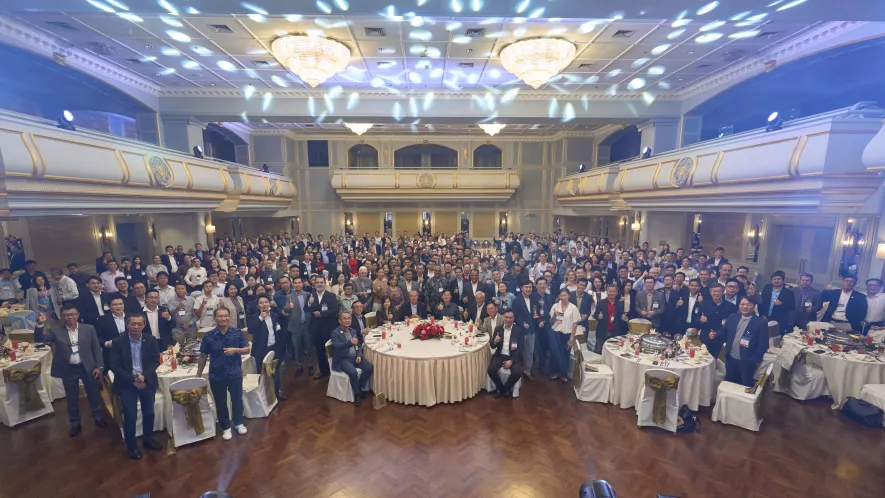
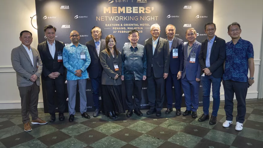
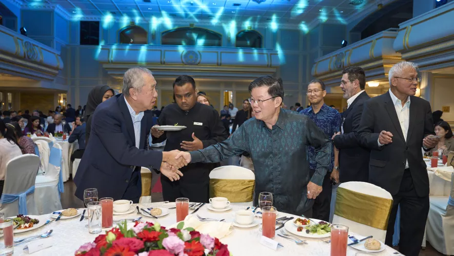
Browse our 2025 SEMI x MSIA Members' Networking Night Photo Gallery

Eastern & Oriental Hotel, Penang | Grand Ballroom
10, Lebuh Farquhar, George Town, 10200 George Town
Pulau Pinang
Malaysia

6:15 pm

Registration & Cocktail Reception

6:45 pm
LindaProfilePhoto_Circle
Ms. Linda Tan

Welcome Speech

Ms. Linda Tan | President, SEMI Southeast Asia

6:50 pm
Dato Seri Siew Hai Wong
Dato' Seri Siew Hai Wong

Welcome Speech

Dato' Seri Wong Siew Hai | President, Malaysia Semiconductor Industry Association (MSIA)

6:55 pm
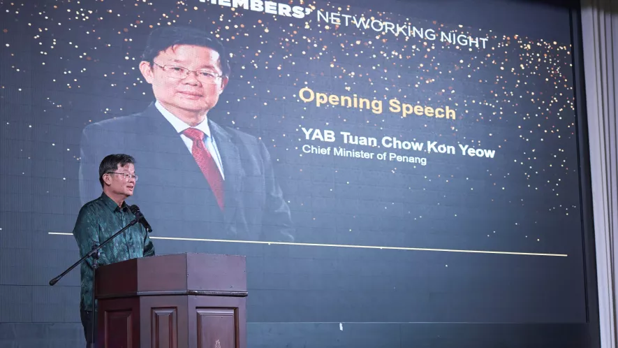
YAB Tuan Chow Kon Yeow

Opening Speech

YAB Tuan Chow Kon Yeow | Chief Minister of Penang

7:05 pm

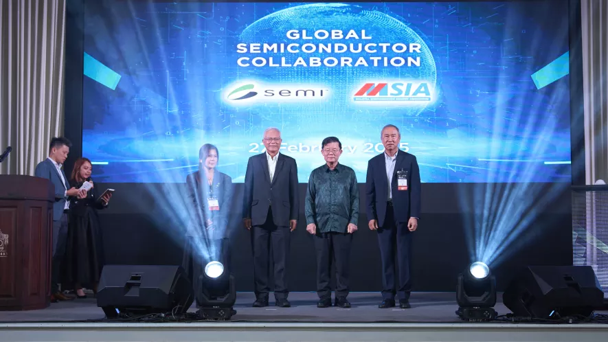
Announcement

Global Semiconductor Collaboration between SEMI SEA and MSIA
Witnessed by YAB Tuan Chow Kon Yeow, Chief Minister of Penang, and Mr. KC Ang, Chairman of the SEMI Southeast Asia Regional Advisory Board.

7:10 pm

Networking Buffet & Drinks

8:00 pm

Live Performance

10:00 pm

End of Networking Night

Program subject to change

Join SEMI Southeast Asia and MSIA for a night of networking and celebration at our exclusive SEMI X MSIA Members' Networking Night. Get a chance to connect with industry leaders, exchange valuable insights, and unlock a myriad of business opportunities.


Members: Free (restricted to 2 representatives per member company)

For additional participants and non-members, please contact [email protected] to discuss applicable fees and arrangements.

Off Add to Calendar 2025-02-27 00:00:00 2025-02-27 00:00:00 SEMI x MSIA Members' Networking Night Join SEMI Southeast Asia and MSIA for a night of networking and celebration at our exclusive SEMI X MSIA Members' Networking Night. Get a chance to connect with industry leaders, exchange valuable insights, and unlock a myriad of business opportunities. Members: Free (restricted to 2 representatives per member company)For additional participants and non-members, please contact [email protected] to discuss applicable fees and arrangements. Eastern & Oriental Hotel, Penang | Grand Ballroom 10, Lebuh Farquhar, George Town, 10200 George Town Pulau Pinang Malaysia SEMI.org [email protected] Asia/Singapore public Asia/Singapore

Registration Details

$39 for SEMI Members (sign into your account with your work email to be recognized)

$59 for non-SEMI Members

Belgium China France Germany Ireland Italy Japan Malaysia Singapore South Korea Taiwan United States Vietnam Register for the 9:00-10:00 AM PT Session Register for the 4:00-5:00 PM PT Session SSI Webinar Series tile 360x317 - Cloned Business Executive
Highlighted content

Abstract

Companies across the semiconductor value chain must respond to a dynamic horizon as the ISSB Standards are adopted by securities regulators, standard-setters and stock exchanges around the world. At the same time, investors are asking companies to voluntarily transition from the TCFD recommendations to the ISSB Standards to meet their information needs.

To clarify what the ISSB Standards mean for the semiconductor value chain, SEMI is pleased to collaborate with the IFRS Foundation, which is the organizational seat of the ISSB. Our webinar, ISSB Standards Adoption and Reporting for the Semiconductor Value Chain, outlines the stakes for companies, demonstrates the business value of the Standards (IFRS S1 and IFRS S2), answers audience questions, and provides a venue for information exchange. There will be a deep dive into implications for climate reporting under IFRS S2 after a high-level look at the background and workplan of the ISSB.

Our distinguished speakers from IFRS Foundation are Neil Stewart, Director of Corporate Outreach, and Jing Zhang, Head of Climate Research.

This event is part of the SEMI webinar series, “Global State of Play: Sustainability Regulations, Reporting, & Incentives.” This series offers semiconductor industry professionals the chance to interact with top-tier experts on the most pressing challenges in compliance, disclosure, and strategy for sustainable business.

Speakers

Neil Stewart

Neil Stewart, Director of Corporate Outreach, IFRS Foundation

Neil Stewart is the International Sustainability Standards Board’s New York-based Director of Corporate Outreach, working with preparers, industry associations, the accounting profession and consultants to build awareness and understanding of the ISSB Standards and SASB Standards. Neil joined SASB in 2020 from Citigroup.


Jing Zhang

Jing Zhang, Head of Climate Research, IFRS Foundation

Jing Zhang is Head of Climate Research on the International Sustainability Standards Board’s technical staff. Previously he was the Global Head of Quantitative Research at Moody’s Analytics. Jing has numerous published books and research papers on financial risk, including the Risk Publications book “Climate Change: Managing the Financial Risk and Funding the Transition.” Jing has a PhD from the Wharton School of the University of Pennsylvania.

United States

Sustainability

Worldwide, companies in the semiconductor value chain are undergoing paradigm shifts in how they report sustainability-related risks and opportunities to stakeholders in government and capital markets.

Semiconductor manufacturing and design firms, together with their business partners, face heightened pressure to report on their performance related to climate transition, human capital management, supply chain management, and a host of other environmental, social, and governance issues.

On one hand, companies face a patchwork of reporting rules conditioned on where they do business. On the other hand,  a global baseline of sustainability-related disclosures ushered in by the IFRS Foundation’s International Sustainability Standards Board (ISSB) is gathering momentum.

Times

Multiple sessions available!
EMEA: Thursday, January 23, 2025 6:00-7:00 pm Central European Time (AM Session - 9:00-10:00 am Pacific)
America:  Thursday, January 23, 2025, 9:00-10:00 am or 4:00-5:00 pm Pacific Time
Asia Pacific: Friday, January 24, 2025 9-10 am Japan Standard Time (PM Session) 4-5 pm Pacific) 
Off Add to Calendar Disabled America/Los_Angeles
Event format

PDF Solutions, Inc. (Nasdaq: PDFS), a leading provider of comprehensive data solutions for the semiconductor and electronics ecosystems, today announced it will host an Executive Conference on the power of AI to transform semiconductor design and manufacturing. This event will take place on December 12, 2024, in downtown San Francisco, CA, following the 70th Annual IEEE International Electron Devices Meeting.

This one-day Executive Conference will feature presentations from PDF Solutions executives, industry thought leaders, solutions partners and customers on the state of art and best practices to design, deploy, scale, and manage trusted AI/ML solutions across the global semiconductor industry.

Additional information including agenda, logistics, and registration, will be available in the coming weeks.

About PDF Solutions
PDF Solutions (Nasdaq: PDFS) provides comprehensive data solutions designed to empower organizations across the semiconductor and electronics ecosystems to improve the yield and quality of their products and operational efficiency for increased profitability. The Company’s products and services are used by Fortune 500 companies across the semiconductor ecosystem to achieve smart manufacturing goals by connecting and controlling equipment, collecting data generated during manufacturing and test operations, and performing advanced analytics and machine learning to enable profitable, high-volume manufacturing.

Registration

For questions or inquiries, please contact: 

Elle Liang

[email protected]

+
Belgium China France Germany India Ireland Italy Japan Malaysia Russia Singapore South Korea Taiwan United States Vietnam 360x317_Event_Calendar_Ad_DAI_Analyzing AI_Driven_v1@2x Business Executive
Highlighted content

The wide adoption of Artificial Intelligence is profoundly impacting many industries, perhaps none more so than the semiconductor industry. Beyond serving as a growth driver for chips across a diverse range of applications, AI and semiconductors are beginning a virtuous cycle where AI is helping to design more powerful chips that in turn enable more advanced AI. The semiconductor industry’s path to $1 trillion in annual revenue by the end of the decade is promising, thanks in large part to AI, but what will that journey actually look like?

This webinar will examine the industry’s AI-driven growth opportunities in depth, while looking at the technological innovation needed to fuel the market expansion. Dr. Handel Jones, CEO of IBS, and author of When AI Rules the World, will share his analysis of how AI will shape the outlook for semiconductor end-markets and segments – along with the race to achieve 1.0nm technology nodes and accelerate the virtuous AI-semiconductor development cycle. He will also cover the future of semiconductor market growth in the AI era as well as areas of opportunities.

About IBS

United States

10:00 am - 10:05 am
Ajit Manocha, SEMI
Ajit Manocha
CEO
SEMI

Welcome Remarks

10:05 am - 10:10 am
Pushkar Apte
Pushkar Apte
Strategic Technology Advisor, Smart Data-AI
SEMI

SEMI Smart Data-AI Initiative and Future of Computing Update

10:10 am - 11:00 am
Handel Jones
Dr. Handel Jones
CEO
IBS

Why AI Will Propel the Semiconductor Market to $1 Trillion and Achieve 1.0nm by 2030

11:00 am - 11:15 am

Q&A

Explore how Artificial Intelligence will impact the semiconductor market through the end of the decade with a deep-dive analysis of the fast-shifting industry landscape focusing in on growth across end markets and segments.

10:00 am - 11:15 am Off Add to Calendar 2024-11-20 10:00:00 2024-11-20 11:15:00 Analyzing AI-Driven Growth: $1T and Beyond Explore how Artificial Intelligence will impact the semiconductor market through the end of the decade with a deep-dive analysis of the fast-shifting industry landscape focusing in on growth across end markets and segments. United States SEMI.org [email protected] America/Los_Angeles public America/Los_Angeles On-demand
Event format
Belgium France Germany India Ireland Italy Japan Malaysia Russia Singapore South Korea Taiwan United States Vietnam Register Now (8-9am PT) Register Now (5-6pm PT) [email protected] Business Executive Featured Speakers
Highlighted content

In today’s fast-paced and interconnected world, the electronics industry faces unprecedented challenges from global disruptions, geopolitical uncertainties, and supply chain vulnerabilities. To remain competitive and resilient, organizations must adopt robust risk management frameworks that proactively identify and mitigate risks.


This webinar is brought to you by the Resiliency Working Group, part of the SEMI Supply Chain Management Initiative. We will explore the creation and implementation of an industry-standard risk management framework tailored to the unique complexities of the electronics supply chain. Attendees will learn how to assess potential risks, develop mitigation strategies, and leverage cutting-edge tools to improve visibility and responsiveness across their supply networks.

Key topics include:


•     The critical risks impacting electronics supply chains and how to address them.
•     Best practices for building a resilient and adaptable risk management framework.
•     Strategies for real-time risk monitoring, supplier risk assessments, and scenario planning.
•     How to align your supply chain with industry standards for business continuity and operational stability.

Who should attend:


•    Supply chain managers
•    Risk officers
•    Operations executives
•    Anyone involved in supply chain planning and resilience in the electronics sector

Join us to discover actionable insights and practical approaches to future-proof your electronics supply chain, ensuring it remains resilient, efficient, and prepared for any disruption.
 

Speaker bio:

Austin Evans is the Director of Supply Chain Risk Management at Intel.  He is responsible for overseeing risk management for Intel’s supply chain as well as Intel’s Contingent Workforce Program Office.  His organization is responsible for business continuity, governance, resilience, supply chain security and compliance. 

United States

Austin Evans.jpg
Austin Evans
Director of Supply Chain Risk Management
Intel
Standards

Join us for a deep dive into the new industry-standard risk management framework tailored to the unique complexities of the electronics supply chain. Hosted by the SEMI Resiliency Working Group, this webinar will equip supply chain professionals with actionable insights on assessing critical risks, developing robust mitigation strategies, and leveraging advanced tools for real-time monitoring.

Off Add to Calendar 2024-10-24 00:00:00 2024-10-24 00:00:00 Building Resilient Supply Chains Join us for a deep dive into the new industry-standard risk management framework tailored to the unique complexities of the electronics supply chain. Hosted by the SEMI Resiliency Working Group, this webinar will equip supply chain professionals with actionable insights on assessing critical risks, developing robust mitigation strategies, and leveraging advanced tools for real-time monitoring. United States SEMI.org [email protected] America/Los_Angeles public America/Los_Angeles
Event format
Belgium China France Germany India Ireland Italy Japan Malaysia Russia Singapore South Korea Taiwan United States Vietnam EMG webinar HI Technical
Highlighted content

Heterogeneous Integration (HI) has come a long way in 50 years. The world of multi-chip modules (MCMs) has given way to a vast ecosystem of chiplets, 3D stacked die, and co-packaging of antenna, high-bandwidth memory (HBM), and optics. HI is at the center of “More than Moore” development activities, as innovative engineers look for creative ways to overcome the slower scaling of silicon technology. The promise of HI is new devices with superior power, performance, area, and cost (PPAC). All these promises come with new challenges. Managing different process nodes, physical characteristics, mechanical stresses, and other system-level challenges not found in monolithic system-on-chip (SoC) devices, creates a great opportunity for design and manufacturing companies to reshape our industry. 


In this webinar, we’ll explore this enabling technology from both the device maker and material supplier perspectives. We will learn about demands placed on devices by new applications and what new tools are needed to meet these demands. We will also hear about the challenges placed on materials and equipment suppliers to develop processes capable of manufacturing the individual components and integrating them into final products. Join us as our panel of experts address the issues and opportunities involved with heterogeneous integration. 
 

United States

Arsalam Alam
Arsalan Alam, PhD
Member of Technical Staff (MTS), 3D Stacking Technology Group
AMD Packaging

2nd Generation 3D V-Cache™ Enablement

Andrea Chacko
Andrea Chacko, PhD
Director of Packaging Solutions
Brewer Science
Dong Shun Bai
Dongshun Bai, PhD
Business Development Director and Senior Technologist of Packaging Solutions
Brewer Science

Enabling Heterogeneous Integration through Material Design

The realization of Heterogeneous Integration (HI) has been key in driving advancements in semiconductor technology. The complexities of integrating dissimilar materials continue to be a challenge for HI. All advanced packaging technologies rely on advanced materials to address the many challenges in achieving continued shrinking and improved performance of devices. Novel materials capable of managing mechanical stresses and increased thermal budgets with strict cleanliness requirements are required for processes such as wafer thinning, fan-out wafer-level packaging, and hybrid bonding. This presentation will highlight how advanced materials can address the growing challenges in the industry.

Andrea Maret
Andrea Maret
Senior Knowledge Manager
Entegris

Webinar Moderator

APHI CAST EHS NBMC Smart MFG SMG Sustainability EMG ESD Alliance FlexTech FOA ITL MSIG SCIS SE&A SiPAT SOI

Dive into the dynamic world of semiconductor materials and discover the future landscape as the industry experts provide a glimpse into the future of the semiconductor ecosystem in the era of heterogenous integration.

10:00 am - 11:00 am Off Add to Calendar 2024-10-16 10:00:00 2024-10-16 11:00:00 Heterogeneous Integration finds its place Dive into the dynamic world of semiconductor materials and discover the future landscape as the industry experts provide a glimpse into the future of the semiconductor ecosystem in the era of heterogenous integration. United States SEMI.org [email protected] America/Los_Angeles public America/Los_Angeles REGISTER NOW
Event format