downloadGroupGroupnoun_press release_995423_000000 copyGroupnoun_Feed_96767_000000Group 19noun_pictures_1817522_000000Member company iconResource item iconStore item iconGroup 19Group 19noun_Photo_2085192_000000 Copynoun_presentation_2096081_000000Group 19Group Copy 7noun_webinar_692730_000000Path
Skip to main content
Default Banner Image

Russia

China Japan Taiwan South Korea Belgium France Germany Ireland Italy Russia India Malaysia Singapore Vietnam Inside_Fab Training

Course Description 

This course provides a comprehensive introduction to semiconductor manufacturing, guiding participants through the complete journey from silicon fundamentals to chip fabrication and packaging. Designed for professionals new to the semiconductor industry, the course explains key concepts, terminology, devices, and manufacturing processes used in modern fabs. 

Who Should Attend

Anyone interested in understanding semiconductor manufacturing, including new employees, professionals in related industries, and those seeking to broaden their knowledge of the field.  

Learning Objectives

Upon completion of the course, participants should be able to:

  • Explain fundamental semiconductor concepts, including silicon materials, doping, PN junctions, and basic device behavior. 
  • Identify and correctly use common semiconductor manufacturing terminology.
  • Outline the key steps involved in front-end wafer fabrication, from bare silicon to patterned wafers.
  • Summarize back-end manufacturing processes, including assembly, packaging, and testing.

Topics Included

  • Basic Electronics and Microelectronics
  • Process Nodes
  • Device Physics and Transistor Operation
  • Crystal Growth and Wafer Preparation
  • Advanced Transistor Technologies
  • Circuit Design and Layout
  • Wafer Processing

Important Information

Note that only the person who registered will receive a certificate of completion. This virtual training will not be recorded. Attendees must be present to access the course knowledge. 

Can't find the training link on the day of the training? After you register, you will receive the link to the live training via the email address you provided. In addition, you will receive email reminders 24 hours in advance and 1 hour before, with the same link. Please keep these emails on hand to access the training on time. If you do not see any confirmation emails, please check your junk/spam folders before contacting SEMI U for support.


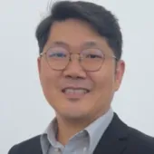
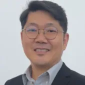
Kalya Shubhakar
Kalya Shubhakar
Senior Lecturer


Singapore

- SEMI U

Strengthen your knowledge and skills by learning about the journey from silicon fundamentals to chip fabrication and packaging. 

Singapore: 3:00pm - 7:00pm

India: 12:30pm - 4:30pm

London: 8:00am - 12:00pm
 

Pricing                     
  • Members:  $399
  • Non-Members:  $449

* For group orders with 10+ attendees, and for Students/Veterans discounted pricing, please contact [email protected]

3:00 pm - 7:00 pm Off Add to Calendar 2026-08-17 15:00:00 2026-08-20 19:00:00 Inside the Fab: An Introduction to Semiconductor Manufacturing (Asia/EU) Strengthen your knowledge and skills by learning about the journey from silicon fundamentals to chip fabrication and packaging. Singapore: 3:00pm - 7:00pmIndia: 12:30pm - 4:30pmLondon: 8:00am - 12:00pm Pricing                     Members:  $399Non-Members:  $449* For group orders with 10+ attendees, and for Students/Veterans discounted pricing, please contact [email protected] Singapore SEMI.org [email protected] Asia/Singapore public Asia/Singapore Register Now
Event format
Promote in calendar
Off

Gütenbach, Germany – December 16, 2025 – RENA Technologies is proud to be a key industrial partner in a new 1.3 million Euro Government-funded project led by the National Physical Laboratory (NPL) and supported by the Department for Science, Innovation and Technology (DSIT). The initiative will establish critical new metrology capabilities to strengthen the UK’s semiconductor innovation infrastructure and accelerate the development and adoption of next-generation semiconductor materials and processes.

This strategic investment underlines the UK’s commitment to maintaining global competitiveness in semiconductors, helping to attract private investment, strengthen supply chains, and support long-term economic growth. As advanced semiconductor materials become central to technologies such as electric vehicles, renewable energy, 5G communications and advanced electronics, robust measurement, verification and standards are increasingly essential.

The project brings together a broad consortium spanning industry and academia. Together, the partners cover the full innovation landscape, from materials research and process development to device fabrication and performance verification.

“At RENA, we develop advanced wet processing and surface treatment solutions that are critical in manufacturing of compound semiconductors and emerging materials. Through this collaboration, RENA will contribute industrial insight and process expertise to ensure that new measurement and testing capabilities are closely aligned with real manufacturing challenges.” States Peter Schneidewind, CEO of RENA Technologies.

While silicon remains the foundation of much of today’s semiconductor industry, many high-growth applications increasingly depend on advanced materials such as gallium arsenide (GaAs), gallium nitride (GaN), silicon carbide (SiC), and indium phosphide (InP). These materials offer superior performance in high-power, high-frequency and optoelectronic applications, but they also introduce new complexities in processing, characterization and quality assurance. Reliable standards and independent measurement methods are therefore essential to derisk innovation and support scale-up.

Through this project, consortium partners will work with NPL to:
• Develop new UK measurement and test capabilities for advanced semiconductor materials by combining academic research excellence with world-leading metrology expertise.
• Apply these capabilities to critical industry challenges, including assessing material integrity, verifying RF performance, and testing device reliability under demanding operating conditions.
• Share the resulting capabilities openly with industry, helping to build national consensus and strengthen the UK’s influence in international standards development for novel semiconductor technologies.

Following extensive consultation the consortium has identified three priority application areas where the UK can have the greatest global impact: power electronics, RF-communications, and optoelectronics. These areas align closely with RENA’s customer base and technology roadmap, particularly in power and compound semiconductor manufacturing.
By participating in this program, RENA reinforces its commitment to supporting the UK semiconductor ecosystem with industrially relevant innovation, enabling customers to adopt advanced materials with confidence, and helping position the UK as a global leader in next-generation semiconductor technologies.

About NPL
The National Physical Laboratory (NPL) is the UK's National Metrology Institute (NMI), developing and maintaining the national primary measurement standards, as well as collaborating with other NMIs to maintain the international system of measurement. As a public sector research establishment, it delivers extraordinary impact by providing the measurement capability that underpins the UK's prosperity and quality of life. NPL develops the metrology required to ensure the timely and successful deployment of new technologies and work with organizations as they develop and test new products and processes.

About RENA Technologies GmbH
RENA Technologies is a leading global supplier of production machines for wet chemical surface preparation. RENA products are used in path-breaking application fields such as semiconductors, MedTech, renewable energies, and the glass industry. RENA equipment is used to treat or modify surfaces of, for example, semiconductor wafers, solar cells, glass, optical substrates or other high-tech products using wet chemical processes. RENA offers proven standard machines as well as customer-specific solutions and process support.


OXFORD INSTRUMENTS PROVIDES COHERENT WITH STATE-OF-THE-ART, FULLY AUTOMATED PROCESSING EQUIPMENT, FOR 6” INP WAFER MANUFACTURING, ENABLING NEXT GENERATION AI APPLICATIONS

Oxford Instruments (OXIG), a leading provider of advanced plasma processing solutions for the compound semiconductor industry, announces the key role it is playing to support the industry’s first fully automated 6-inch indium phosphide (InP) wafer fabrication capability for photonic devices, led by Coherent Corp. (NYSE: COHR), a global leader in compound semiconductors and high-performance optical networking solutions.

Oxford Instruments’ cutting-edge plasma processing equipment is central to Coherent’s groundbreaking achievement of ramping up 6-inch InP fabs in Sherman, Texas, and Järfälla, Sweden. These fabs will play a pivotal role in driving advancements in AI datacentre, telecommunications, and sensing applications. Coherent’s transition to 6-inch wafers is set to deliver significant benefits, including a substantial increase in capacity, lower die cost and more than four times the number of devices per wafer.

Oxford Instruments has supplied fully automated, high-throughput 6-inch InP processing equipment, enabling Coherent to achieve these remarkable productivity gains. This advanced equipment is designed to support the transition from 800G to 1.6T products, a key requirement to meet the growing demands of AI interconnects and optical communications.

“We have been the leading supplier of InP plasma etch equipment to the datacom market, and Coherent, for many years. Our technology, with the quality, throughput and reliability that we have developed alongside excellent service, is ideally positioned to support the current device demand inflection we are seeing with the release of generative AI applications. We are delighted to be partnering with Coherent during this exciting period of market expansion and look forward to continuing to develop and release innovative and valuable plasma processing solutions.” Matt Kelly, Managing Director, Oxford Instruments Plasma Technology.

"Coherent’s move to 6-inch InP wafer fabrication marks a transformative milestone for the industry. Oxford Instruments’ expertise in plasma processing has been essential in enabling our Sherman and Järfälla fabs to reach world-class performance,” said Dr. Beck Mason, Executive Vice President – Semiconductor Devices at Coherent. “Together, we are advancing InP technology to support faster networks, greater efficiency, and the new applications that will define the future of connectivity."

The joint efforts of Oxford Instruments and Coherent have culminated in a manufacturing platform that sets the stage for the next generation of InP optoelectronic devices. These devices are critical enablers for applications ranging from AI datacentres and datacom transceivers to advanced sensing in consumer electronics and automotive technologies.

Nijmegen, October 20, 2025 – Chip Integration Technology Center (CITC) will become part of TNO. This strategic move marks a significant step toward ensuring the long-term continuity and stability of CITC’s research and operations. The integration emphasizes TNO’s ambition to take a leading position in the innovation of chip packaging technologies and strengthen the regional semiconductor ecosystem in Nijmegen.

“In the coming years, TNO aims to play a key role in the development of advanced chip packaging in the Netherlands,” says Arnaud de Jong, director of High Tech Industry at TNO. “By integrating CITC into TNO, we can intensify and expand our research efforts. We also contribute to the further development of Lifeport in Nijmegen as a strong, future-proof semiconductor ecosystem.” With the investment in CITC, TNO connects chip technology activities between Nijmegen and other semiconductor hubs such as Eindhoven.

Advanced chip packaging
CITC was founded in 2019 by TNO and Delft University of Technology (TU Delft), among others, as an independent innovation center for advanced chip packaging technology. Within an ecosystem of companies, research institutions and educational organizations, CITC has developed into a broad R&D hub that collaborates on technological breakthroughs in advanced chip packaging.

“CITC’s integration into TNO marks a noteworthy moment for CITC. This step underscores our shared vision for the future of chip integration and packaging technology,” says Jeroen van den Brand, general manager of CITC in Nijmegen. “This provides room for growth, accelerates innovation, and strengthens CITC’s international position as a center of expertise for chip packaging.”

Strategic choice for Nijmegen
CITC’s integration into TNO will formally take effect on January 1, 2026. CITC will become part of TNO’s High Tech Industry business unit and will remain located at the Noviotech Campus in Nijmegen. Toni Versluijs, chairman of the CITC Supervisory Board: “CITC continues on its current course. For the Supervisory Board, it is essential that, with TNO’s ambition and investment, we secure continuation of the CITC activities, while building on the existing talent and technology and give CITC room to grow further.”

Lucas van Vliet, member of the CITC Supervisory Board on behalf of TU Delft: “The collaboration between TU Delft and TNO within CITC will change form as of January 1 but remains as strong as ever. TU Delft believes in the importance and growth potential of chip packaging and sees incorporating CITC into a strong organization like TNO as an opportunity to further accelerate innovation in chip technology.”

- ENDS -

About CITC
CITC is a non-profit, joint innovation center specializing in heterogeneous integration and advanced chip packaging technology. With the aim of bridging the gap between academia and industry, CITC has created an effective ecosystem where companies, research and educational institutions collaborate. CITC was founded in 2019 with strategic partners TNO and Delft University of Technology and is supported by the province of Gelderland and Nijmegen municipality. Located on Noviotech Campus Nijmegen, CITC is perfectly situated in the heart of the Dutch semiconductor industry.
www.citc.org

About TNO
TNO is the largest independent research and technology organization in the Netherlands and one of the largest in the EU. We innovate, investigate, and orchestrate, collaborating closely with governments, universities and the private sector. We inform government on policies and empower evidence-based decision-making through rigorous investigations, cutting-edge scientific insights, and reliable measurements. By building national and international consortia and ecosystems, we drive technological and methodological breakthroughs that help to realise a secure, sustainable, healthy, and digital society, and strengthen the earning power of the Dutch economy.
www.tno.nl/en/

Contact
Christian Ketelaars, Communications Manager
E [email protected]
M +31 (0)6 48 15 42 92

Belgium France Germany India Ireland Italy Japan Malaysia Russia Singapore South Korea Taiwan United States Vietnam Webinar_2025-SCM_360x317_Event_Calendar_SCM_2025 Business Executive Technical
Highlighted content

Join us for an insightful webinar as we present the findings from the 2025 Semiconductor Supply Chain Survey, a collaborative effort between the SEMI Supply Chain Management initiative and McKinsey & Company.

The annual survey aims to establish benchmarks for operational agility metrics, covering the entire value chain from material suppliers to OEMs, offering a comprehensive view of the landscape. New this year are additional insights on trends in LTAs and organizational supply chain management capabilities

During this webinar, we will share results from the survey uncovering key trends, challenges, and opportunities within the semiconductor supply chain. By attending, you'll gain valuable insights to benchmark your organization against peers, identify areas for improvement, and course-correct more effectively. Please contact us if you like to learn about how your company can participate in the SCM initiative.

United States

SCM

Join us for a webinar highlighting the 2025 Semiconductor Supply Chain Survey results, conducted by SEMI SCM initiative and McKinsey & Company. Gain fresh insights into operational agility, LTAs, and SCM capabilities across the value chain. Discover key trends, challenges, and opportunities to benchmark your organization and strengthen supply chain resilience.

Choose your session:

9:00 am - 10:00 am Off Add to Calendar 2025-09-23 09:00:00 2025-09-23 10:00:00 2025 Semiconductor Supply Chain survey: Insights for strategy and capabilities Join us for a webinar highlighting the 2025 Semiconductor Supply Chain Survey results, conducted by SEMI SCM initiative and McKinsey & Company. Gain fresh insights into operational agility, LTAs, and SCM capabilities across the value chain. Discover key trends, challenges, and opportunities to benchmark your organization and strengthen supply chain resilience.Choose your session:US/EU: 9:00 AM – 10:00 AM PT [ Register Now ]Asia/US: 5:00 PM – 6:00 PM PT [ Register Now ] United States SEMI.org [email protected] America/Los_Angeles public America/Los_Angeles

Speakers


Henry Marcil

Partner

McKinsey & Company

Bio: Leader in McKinsey’s Advanced Industries Practice, focused on semiconductors n and key end markets (e.g., high tech)

Leads McKinsey’s Resiliency and Geopolitics service line in Semiconductor


Kushal Jolapara

Engagement Manager

McKinsey & Company

Bio: Manager in McKinsey's Operations practice, with a focus on product development and procurement service lines

Leads Supply Chain studies for Advanced Industries clients including Aerospace, Auto and Semiconductors

Dan Peacock

Engagement Manager

McKinsey & Company

Bio: Manager in McKinsey’s Operations Practice, focused on procurement and capital projects

Leads Operations projects at Foundries, IDMs, and equipment clients


Event Contact:

Krish Dharma

[email protected]

Agenda

•    Lead times throughout the semiconductor value chain
•    Landscape and trends in purchasing agreements and LTAs
•    Demand forecasts, backlogs, and end markets
•    Market outlook, opportunities, and threats
•    New for 2025: Organizational capabilities in supply chain management

Event format
Tab Order
Overview
New Tab 2
New Tab 1
Registration
Promote in calendar
Off

Registration for the Global Executive Summit is closed.  Please contact Heidi Hoffman at [email protected] with any questions.  

Belgium France Germany India Ireland Italy Japan Malaysia Russia Singapore South Korea Taiwan United States Vietnam 360x317 GES25 Executive

SEMI Japan has included the Okura Hotel and 3 other hotels convenient to the Okura in the Hotel Block for SEMICON Japan - taking place December 17-19 at Tokyo Big Sight.  View the hotels and rates HERE.

Google Link
Highlighted content

Building on the foundational work of the SEMI Sustainability Climate Consortium and the 2025 Global Climate Summit Workshops (GCSW), this closed-door summit is designed to shift our industry from alignment to action. We are convening a select group of key Executive decision makers & senior leaders from fabs, fabless companies, hyperscalers, and key suppliers and energy partners to: 

  • Showcase and accelerate progress on priority climate initiatives: Abatement, Gas Substitution, Green Materials, and Energy
  • Define clear deliverables and next-phase commitments that unlock scale and momentum
  • Strengthen executive collaboration to remove barriers, share ownership, and drive measurable results

This Summit is not about what we could do — it’s about what we will do, and who will lead.

Click here for the Executive Briefing outlining the event objectives, and the action pathways and methods of engagement for all attendees.  Plan ahead on how presence can shape outcomes that accelerate our industry's decarbonization.

Okura Hotel
Tokyo
Japan

Monday, December 15, 2025

9:00 am - 9:20 am

Coffee & Registration

9:25 am - 9:30 am
 Masahiko (Jim) Hamajima - President, SEMI Japan
Jim Hamajima
President
SEMI Japan

9:30 am - 9:45 am
Ajit Manocha, SEMI
Ajit Manocha
CEO & President
SEMI
Carolin Seward, Google
Carolin Seward
VP of Custom Silicon Sourcing and Operations
Google

GES Opening

9:45 am - 10:25 am
Carolin Seward, Google
Moderator
Carolin Seward
Google
Jinman Han
Jinman Han
President
Samsung Foundry
Jens Liebermann
Jens Liebermann
Senior VP of Global Business
BASF
Sundeep Bajikar
Sundeep Bajikar
Corp. VP Head of Corp Strategy
Applied Materials
Sam Naffziger
Sam Naffziger
SVP & Fellow of Product Technology Architecture
AMD

Fireside Chat: Bending the Curve of Emissions Through Industry Collaboration

Join senior executives from Apple, Samsung Foundry, BASF and Applied Materials, for a discussion on the partnerships required to meaningfully bend the curve towards decarbonization. In an industry already operating under tremendous constraints, what are the lower hanging fruits that are ripe for intentional, precompetitive collaboration? And what can be solved independently?

10:25 am - 10:40 am
Sam Naffziger
Sam Naffziger
SVP & Fellow of Product Technology Architecture
AMD

Spotlight: AMD on the role of Silicon Design for Energy Efficiency

Discover how fabless leaders are driving decarbonization through innovations in energy-efficient product architecture and the critical role of silicon design in minimizing "Use Phase" emissions, the largest contributor to a chip's carbon footprint.

10:40 am - 11:10 am
Anne Meegan
Moderator
Anna Meegan
Director of Sustainability
Google Platforms & Devices
Angela Baker
Angela Baker
VP Sustainability
Qualcomm
Dharmesh Jani
Dharmesh Jani
Director, AI Infra Ecosystem & Partnerships
Meta
Cooper Elsworth
Cooper Elsworth
Sr. TPM, Advanced Energy Labs
Google

End-User Panel: The Decarbonization Imperative

Hear from technology leaders at AMD, Qualcomm, Meta, and Google on why accelerated decarbonization is a business imperative. This panel explores how end-users are (1) acting with a sense of urgency, (2) engaging and enabling their supply chains, (3) driving energy efficient design to drive innovation to accelerate collective progress.

11:10 am - 11:25 am

Break

11:25 am - 11:30 am
Bruce Gall Google
Bruce Gall
Strategic Partnerships
Google

Overview of Priority Initiatives

Priority Initiative: Fab Upstream Materials

11:30 am - 11:40 am
Saifi Usmani, EMD Electronics
Saifi Usmani
VP Global Sustainability
SEMI

Opening Remarks

From Fragmentation to Focus: Outlining a strategy to activate the fab supply chain with a unified customer voice and collaborative support.

11:40 am - 12:10 pm
Bessima
Bessma Aljarbou
Head of Strategy of Environment & Supply Chain Innovation
Apple, Inc.

Keynote: Apple's Supply Chain Engagement

Hear from Apple senior leadership on supply chain engagement and decarbonization, using commercial levers and the power of support and collaboration.

12:10 pm - 12:40 pm
Handy Ko TSMC
Handy Ko
Director, Materials Management
TSMC

From Ambition to Action: A Fab's Role in Upstream Decarbonization

Hear about TSMC's upstream scope 3 (supply chain) decarbonization leadership and recognition of the business imperative, which have been embedded into their core supplier engagement program.

12:40 pm - 12:55 pm
Andrea Jorissen
Andrea Jorissen
Supplier Carbon Solutions
Apple, Inc.

Solutions Enablement & Calls-to-Action

Highlighting clean energy advanced procurement academies and demand aggregation case studies. Announce renewed ambitions and goals for fab upstream scope 3 decarbonization.

12:55 pm - 1:55 pm

Networking & Lunch

Priority Initiative: Clean Electricity

1:55 pm - 2:05 pm
Rebecca Green
Rebecca Green
Partner
ERM
Ken Haig
Ken Haig
Senior Director Government Affairs
Microsoft

Opening Remarks

Setting the stage for collective action on clean electricity in Asia.

2:05 pm - 2:30 pm
Patrick Tan
Patrick Tan
Head of Wider Asia, APAC
Aurora Energy Research

From Visibility to Viability: Developer Insights on Building a Net Zero Future

Hear a market outlook on Clean Electricity in Korea, Japan, and Taiwan, examining current barriers to renewable expansion and the major opportunities driving investment and clean energy growth through 2030.

2:30 pm - 2:55 pm
William Hudson
Will Hudson
Director, Energy & Sustainability Policy
Microsoft

Keynote: Clean Electricity Policy Action & Urgency

Accelerating Clean Electricity expansion requires clear, coordinated policy action. By uniting around shared advocacy priorities, industry and government can remove barriers, unlock renewable supply, and strengthen cost competitiveness across Korea, Japan, and Taiwan.

2:55 pm - 3:25 pm
YS Kim SK HYNIX
Yong Sung Kim
Head of Clean Energy
SK Hynix

Deep Dive: A Clean Semiconductor Partnership in Korea

Explore the proposed Clean Semiconductor Partnership (CSP), SEMI’s flagship initiative to accelerate Clean Electricity development in Korea by aligning industry, government, and utilities on policy reform and procurement innovation, creating a model for collaborative clean energy expansion across Asia.

3:25 pm - 3:40 pm
William Hudson
Will Hudson
Director, Energy & Sustainability Policy, Asia Pacific
Microsoft

Calls to Action

From discussion to action, secure collective advocacy priorities, resource commitments, and endorsement of the Clean Semiconductor Partnership as the pilot for accelerating Clean Electricity expansion across the region.

3:40 pm - 4:10 pm

Break

4:10 pm - 4:50 pm
Rebecca Green
Moderator
Rebecca Green
ERM
Josh Seidenfeld
Josh Seidenfeld
Supply Chain Clean Energy Lead
Google
Chikako Matsumoto
Chikako Matsumoto
Director, Managing Executive Officer
Sumitomo Mitsui Trust Group
Rei Ushikubo
Rei Ushikubo
Director and Head of the Carbon-Free Solutions Division
Shizen Energy
Daisuke Tsujimoto
Daisuke Tsujimoto
Executive Officer, CSO
Renova Inc.

Day 1 Closing Panel: Accelerating Affordability: Scaling Clean Energy Through Collaboration.

How banks, fabs, and retailers can work together to lower renewable energy prices and spread risk, while examining how AI and digital innovation can accelerate price reductions across the supply chain, grid integration, and project development.

4:50 pm - 5:00 pm
Saifi Usmani, EMD Electronics
Saifi Usmani
Vice President, Sustainability
SEMI

Day 1 Closing Remarks and Look Ahead

Reflect on the day's takeaways and action items.

5:00 pm - 6:00 pm

Member-to-Member Meetings / Break

6:00 pm - 6:30 pm

Networking Reception

Join us for Networking in the Orchard Foyer

6:30 pm - 8:30 pm
Alison Drury
Alison Drury
Global Technology Industry Lead
ERM

Dinner with Fireside Chat: “2030 in Focus: Choices That Will Define a Decade”

A forward-looking conversation on how the semiconductor industry can navigate the convergence of climate action, geopolitics, and AI to define its leadership in 2030.

Tuesday, December 16, 2025

8:30 am - 9:15 am

Coffee & Networking

9:15 am - 10:00 am
Saifi Usmani, EMD Electronics
Saifi Usmani
VP Global Sustainability
SEMI

Day 2 Opening

Opening remarks will summarize Day 1 and preview Day 2.

9:30 am - 10:00 am
Lora Ho
Lora Ho
SVP Strategy & ESG
TSMC

TSMC Keynote

Hear from industry leader TSMC on their strategy for decarbonizing advanced semiconductor manufacturing and how it connects to the four GES Priority Initiatives including a new, collaborative path to scale low-GWP gas substitutions from R&D to high-volume manufacturing.

10:00 am - 10:15 am

Break

Priority Initiative: Gas Substitution

10:15 am - 10:25 am
Bruce Gall Google
Bruce Gall
Strategic Partnerships
Google

Opening Remarks

Current efforts to pursue low Global Warming Potential (GWP) gas substitutions in etch and chamber clean applications remain fragmented, resulting in high material costs for HVM application. While promising gas substitutions exist, the traditional paths of small scale or single customer adoption are typically too expensive due to cost scaling limitations. So how do we enable low GWP gas substitutions that also meet cost (as well as performance) expectations? By coordinating a fab-led, industry wide approach to
1) Prioritize a single, low GWP target gas for replacement
2) Co-create and execute a phased experimental plan

10:25 am - 10:45 am
Vahid Vahedi, PhD
Vahid Vahedi
CTO
Lam Research

Equipment Perspective: Scaling Low-GWP Gas Substitution

Hear from a top equipment leader on the process innovations and industry collaboration required to scale low-GWP gas substitution from R&D to high-volume manufacturing

10:45 am - 11:05 am
Steven Scheer
Steve Scheer
SVP Compute System Scaling
imec

imec’s Gas Assessment Platform for Sustainability (GAPS) 

Learn about imec’s Gas Assessment Platform for Sustainability (GAPS) project and how it can be leveraged as an industry test bed for low GWP gas substitution

11:05 am - 11:35 am
Bruce Gall Google
Moderator
Bruce Gall
Google
Rachel Potter EMD
Rachel Potter
VP of Specialty Gas
EMD / Merck
Vahid Vahedi, PhD
Vahid Vahedi
CTO
Lam Research
Steven Scheer
Steve Scheer
SVP Compute System Scaling
imec

It Takes an Ecosystem: A Value Chain Panel on Accelerating Low-GWP Adoption

Hear perspectives from leaders in electronic design automation (EDA), materials, and equipment OEMs on the challenges and opportunities in driving industry adoption of low GWP gases

11:35 am - 11:45 am
Bruce Gall Google
Bruce Gall
Strategic Partnerships
Google

Calls to Action

From Commitment to Action: Outlining the roadmap and action plan for the Gas Substitution Initiative.

11:45 am - 12:45 pm

Networking Lunch

Priority Initiative: Abatement

12:45 pm - 1:10 pm
Beth Elroy
Elizabeth Elroy
VP Sustainability
Micron

Opening Remarks & Keynote

Industry-wide collaboration is critical to accelerate technology innovation and unlock scalable, cost-effective abatement solutions to ease abatement deployment challenges on cost, facilities, space, utilities and operational complexity. Micron will deliver a keynote sharing the abatement journey and the state of current efforts in emission measurement.

1:10 pm - 1:50 pm
Josh Robbins
Moderator
Josh Robbins
Google
Phil Kester
Phil Kester, PhD
Senior Chemical Engineer
Guild Associates
HK KIM KIMM
Dr. Hak-Joon Kim
Korea Institute of Machinery & Materials

F-GHG Catalyst Development & Funding Vehicles

Catalytic abatement remains an important technology, but further research and efforts are needed to identify new catalytic materials, scale performance, and improve their recyclability. Hear from a leading fab and a leading catalyst developer and learn about a promising funding opportunity lead by the Korean government.

1:50 pm - 2:20 pm
Yong Keong Goh
Moderator
Yong Keong Goh
Senior Manager
Micron
Martin Tollner
Martin Tollner
President, Semiconductor Division
Edwards
Morihara Kanken
Atsushi Morihara
Chief Technical Officer
Kanken
Rene Reichardt
Rene Reichardt
CEO
DAS EE
Jong Pil Yoon
Jong Pil Yoon
President
EcoEnergen

F-GHG and Nitrous Oxide Abatement Technology Panel

Abatement technologies are advancing rapidly, and new breakthroughs are on the horizon. Engage with leading abatement suppliers on their outlook on technology roadmaps, strategic priorities and collaborative opportunities.

2:20 pm - 2:30 pm
Kongyeong Goh
YongKeong Goh
Micron
Josh Robbins
Joshua Robbins
Google

Closing Remarks: Abatement

Call-to-actions for commitment to drive high efficiency and low-fuel abatement solutions to accelerate carbon footprint reduction and commercialization, and advance emission measurement technologies to simplify performance verification.

2:30 pm - 2:45 pm
Saifi Usmani, EMD Electronics
Saifi Usmani
VP Global Sustainability
SEMI

Calls to Action Summary & Closing

Hear the takeaways from the Summit and actions for moving forward in our decarbonization journey.

- Sustainability

Semiconductor value-chain executives will gather to align on key initiatives and calls to action, based on our shared decarbonization ambitions, insights and progress thus far.  Together, we will forge an actionable plan for global industry collaboration in three focus areas:  direct emissions, energy-related emissions, and reporting.  This invite-only event will be conducive to accelerating the decarbonization across the industry.

9:00 am - 5:00 pm Off Add to Calendar 2025-12-15 09:00:00 2025-12-16 17:00:00 Global Executive Summit Tokyo 2025 Semiconductor value-chain executives will gather to align on key initiatives and calls to action, based on our shared decarbonization ambitions, insights and progress thus far.  Together, we will forge an actionable plan for global industry collaboration in three focus areas:  direct emissions, energy-related emissions, and reporting.  This invite-only event will be conducive to accelerating the decarbonization across the industry. Okura Hotel Tokyo Japan SEMI.org [email protected] Asia/Tokyo public Asia/Tokyo
Event format
Promote in calendar
Off

Martinez, CA—EUV Tech (EUVT), a global leader in designing and manufacturing at-wavelength EUV metrology equipment, is excited to announce the release of the FALCON Photoresist Flood Exposure Tool. As our next-generation EUV resist characterization and diagnostics tool, FALCON allows photoresist manufacturers to rapidly and accurately test EUV resist sensitivity, as well as providing patterning materials developers critical insights into exposure mechanisms.

Built upon EUV Tech’s proven resist tool technology, FALCON is a fully automated tool that supports high-throughput contrast curves on EUV-patterning materials and radiation chemistry diagnostics by integrating a wide variety of optional add-on analysis and processing modules.

Enhancing FALCON’s platform is an array of in-situ analysis and process modules, including Fourier Transform Infrared (FTIR) Spectroscopy, Atomic Mass Spectrometry, Total Electron Yield (TEY), Photo-Electron Spectroscopy (PES), environmental and vacuum bake module with additional diagnostics, and a scanner-environment exposure module.

Key to FALCON’s effectiveness is its highly uniform exposure spot size of 6 mm, supporting high-sensitivity chemical analysis and over 1,000 exposures for a 300 mm wafer in a single recipe run. Built-in data visualization tools make it possible to analyze this rich data. Combining uniformity, high configurability, and deep data collection and analysis makes FALCON a highly efficient, cost-effective tool for advanced photoresist development.

For more information on the enhanced FALCON Flood Exposure Tool or any of EUV Tech’s at-wavelength metrology tools, please visit euvtech.com.

About EUV Tech
EUV Tech enables technology advancement in the frontiers of semiconductor manufacturing and material science through the development of world-leading EUV and soft-x-ray instrumentation and techniques.

For further information, contact:
EUV Tech, Inc.
[email protected]
+1 (925) 229-4388

Belgium China France Germany India Ireland Italy Japan Malaysia Russia Singapore South Korea Taiwan United States Vietnam Webinar-Critical Minerals-v1_360x317_Event_Calendar_CM Business Executive Technical
Highlighted content

As world leaders act to secure access to these minerals, companies come under pressure to follow due diligence guidelines to promote ethical sourcing of these materials for their supply chains.  Regulations such as the US Dodd-Frank Wall Street Reform and Consumer Protection Act (Section 1502), EU Regulation 2017/821 and the EU Corporate Sustainability Due Diligence Directive require companies to trace materials through their supply chains and report to the public about their use of conflict minerals. 

Several industry associations, including the Responsible Business Alliance’s Responsible Minerals Initiative, were created to help companies with their due diligence efforts. Reports such as those issued by the US Government Accountability Office on Conflict Minerals offer insights into the efficacy of these regulations and suggest improved approaches for industry engagement. 

The SEMI Responsible Supply Chain (RSC) working group was recently formed to host discussions on these topics. This webinar will provide insights from speakers Jennifer Peyser, Responsible Business Alliance Senior Vice President of Responsible Sourcing, and Kimberly Gianopoulos, Managing Director for the International Affairs and Trade team at the U.S. Government Accountability Office (GAO).

United States

8:00 am - 8:05 am
Kim Harrison
Dr. Kimberly Harrison, Ph.D
Senior MEMS Engineer
AMFitzgerald & Associates

Welcome and Introductions of RSC working group

Dr. Harrison is a MEMS Engineer with AMFitzgerald & Associates, a design firm located in the Bay Area California. She has a doctoral degree in mechanical engineering from Stanford University, and has worked as a designer and process engineer in the semiconductor industry for 10 years. She was nominated as a 2022 MEMS & Sensors Industry Group Emerging Leader. As a founding member and leader of the SEMI Responsible Supply Chain Working Group, she hopes to bring SEMI members together to discuss solutions to human rights issues in the semiconductor supply chain.

Conflict Minerals Supply Chain Overview

8:05 am - 8:35 am
Kimberly Gianopoulos
Managing Director for the International Affairs and Trade
U.S. Government Accountability Office (GAO)

Report Review

Director Gianopoulos oversees a 140-person team that reviews a wide variety of federal government oversight issues, including International Security Assistance, Bilateral and Multilateral Foreign Assistance, International Trade and Finance, and U.S. Diplomatic Presence and Management. She serves as a facilitator in GAO’s Learning Center and participates in recruiting activities. Ms. Gianopoulos has received several awards, including a Distinguished Service Award, a Meritorious Service Award, a Client Service Award, and several Results Through Teamwork awards. Ms. Gianopoulos earned a Bachelor’s degree in Mathematics and a Master’s degree in Public Analysis and Administration from the State University of New York at Binghamton. She is a Certified Government Financial Manager and a member of Pi Alpha Alpha, the Global Honor Society for Public Affairs and Administration.

Jen Peyser
Jennifer Peyser
Executive Director
Responsible Minerals Initiative

RMI Activity Overview

“The RMI supports over 500 downstream, midstream, and upstream member companies with a suite of due diligence standards and tools, data, guidance, training, and other resources for global responsible sourcing and regulatory compliance. Our facility and supply chain due diligence standards are rooted in longstanding international norms while reflecting emerging corporate and stakeholder priorities for regulatory compliance, managing sustainability risks and impacts, and fostering responsible mineral supply chains.”

8:35 am - 8:55 am

Q&A

8:55 am - 9:00 am

Summary and Closing Remarks

SCM 8:00 am - 9:00 am Off Add to Calendar 2025-07-09 08:00:00 2025-07-09 09:00:00 Critical Minerals, Due Diligence and the Semiconductor Supply Chain United States SEMI.org [email protected] America/Los_Angeles public America/Los_Angeles Register for On-demand
Event format
Promote in calendar
Off

Test Research, Inc. (TWSE: 3030), the leading test and inspection systems provider for the electronics manufacturing industry, is proud to announce its successful partnership with Bosch in the development of an AI visual check solution for MEMS packaging.

Bosch has recognized TRI's valuable contribution to their success in MEMS packaging in 2025 with a Certificate of Appreciation. The certificate acknowledges the successful completion of the AI visual check for MEMS packaging, highlighting the strong cooperation and partnership between the two companies.

This collaboration demonstrates TRI's expertise in AI-driven inspection solutions and its commitment to providing valuable solutions for the electronics manufacturing industry. TRI's AI-powered solutions include the AI Defect Detection, AI Smart Programming, AI Verify Host, AI training tool, AI Station, and more.

Please visit the following link to learn more about TRI's AI Solutions:
https://www.tri.com.tw/en/about/about-107-2-2.html

Learn more about the Bosch Group by following the link below:
https://www.bosch-presse.de/pressportal/de/en/company-page.html

###

About Test Research, Inc. (TRI)

TRI (TWSE: 3030), offers the most robust product portfolio in the industry for Automatic Test and Inspection solutions. Learn more at http://www.tri.com.tw. For sales and service information, please write to us at [email protected] or call +886-2-2832 8918.

Stanton Chase is pleased to announce that Sundar Rajan Ramalingam has joined the firm as a Partner in North America. His addition strengthens the firm's executive search and leadership consulting capabilities for the semiconductor sector at a time of rapid transformation.

Sundar brings nearly three decades of leadership experience across manufacturing and global technology sectors. He has scaled a multi-billion-dollar global engineering division and supported the growth of several Global Capability Centers (GCCs). Within the semiconductor ecosystem, he has played a pivotal role in building and advising leadership teams across chip design, chip-to-cloud platforms, semiconductor fabs, and foundry operations.

This deep operational and strategic background gives Sundar a unique perspective on the evolving talent needs of semiconductor organizations.

"The semiconductor industry is entering a pivotal era—what I call a 'perfect leadership storm'—driven by generative AI, strategic autonomy imperatives, and breakthroughs like 3nm and advanced packaging," said Sundar. "While these trends are accelerating innovation, the industry also faces a growing talent gap. Companies need capable leaders who can navigate complexity, scale innovation, and build resilient teams. I plan to use my experience in technology and manufacturing to help semiconductor companies find executives who deliver results and foster sustainable growth."

Sundar's career spans both strategic HR leadership and general management with P&L responsibility, offering clients a rare blend of technical insight and leadership development expertise.

"Sundar fits well with our North American team and fills a specific need in our practice," said Mickey Matthews, Managing Director at Stanton Chase in North America and Chair of the Governance Committee. "His time working across borders gives him a genuine understanding of how global teams function. Blending this multicultural understanding with Sundar's deep technology products and services vertical expertise matters a lot to the clients we serve and specifically in the semiconductor space."

Jan-Bart Smits, Managing Partner at Stanton Chase Amsterdam and Global Sector Leader for Semiconductors, added: "Sundar joins us when the semiconductor industry sits at a turning point. Firms in this sector are looking for something different in their executives—people who understand both market forces and engineering details. Sundar knows this world and will further enhance our ability to serve chip makers and their suppliers."

As the semiconductor industry moves into a new chapter—marked by AI-driven demand, geopolitical shifts, and the race toward next-gen nodes—Sundar's appointment signals Stanton Chase's commitment to helping clients lead with confidence and clarity.

Sundar holds an MBA from XLRI Jamshedpur (India) and completed executive education programs, including the Chief Human Resource Officer Program at Wharton, University of Pennsylvania.

He will serve clients from Stanton Chase offices in Baltimore and Raleigh, USA, as well as Bangalore, Hyderabad, and Chennai, India—locations near semiconductor business centers.

Click here to learn more about Sundar.

Click here to learn more about Stanton Chase's semiconductor expertise.

About Stanton Chase

Stanton Chase ranks among the top global retained executive search firms with more than 76 offices in 45 countries and a worldwide team of senior consultants. Stanton Chase serves clients across multiple industry specialties and places C-suite executives, senior managers, and board members for companies ranging from global corporations to emerging businesses. Stanton Chase belongs to the Association of Executive Search and Leadership Consultants (AESC), adhering to the highest industry standards of professionalism and ethics.