downloadGroupGroupnoun_press release_995423_000000 copyGroupnoun_Feed_96767_000000Group 19noun_pictures_1817522_000000Member company iconResource item iconStore item iconGroup 19Group 19noun_Photo_2085192_000000 Copynoun_presentation_2096081_000000Group 19Group Copy 7noun_webinar_692730_000000Path
Skip to main content
Default Banner Image

Malaysia

Malaysia Singapore APS Workshop Mar 2024 Executive Technical

Supporting Partners

HRDC_2023
InvestPenang_logo_2022
MSIA_logo_2022
Featured Speakers
Highlighted content

This course will cover:

  • Evolution of IC Packaging – Fan-in, Fan-out WLP, Embedded Packaging technology, System on Chip (SOC), System in Package (SiP), 3D IC, WLP, TSV etc.
  • Principles of Interconnects ranging from TAB, Wirebond to various Flip Chip bonding such as thermocompression bonding with NCP, C4, ACF for manufacturing and R&D development
  • Board level assembly and its soldering materials and failure mechanisms for 2nd level interconnect
  • Overview of interposer of lead frame, ceramic, flex to BT substrates for Microelectronics Packaging
  • Assembly flow and new assembly techniques such as stealth dicing, compression molding, underfill molding etc., and its assembly materials for Microelectronics packaging
  • Material characterization from bulk to interfaces for Microelectronics packaging

Why should I attend?

  • Gain technical knowledge for industry professionals
  • Enhance knowledge in manufacturing and R&D know-how in IC packaging
  • Apply Key Technical Concepts in Problem Solving through Real Case Studies
  • Networking opportunities with industry peers

Who should attend?

  • Beneficial for directors, managers, process & equipment engineers, R&D engineers and Quality & Reliability engineers working in the areas of microelectronics packaging
  • Useful for sale or application engineers who supply packaging materials and tools to the industry

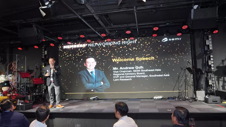
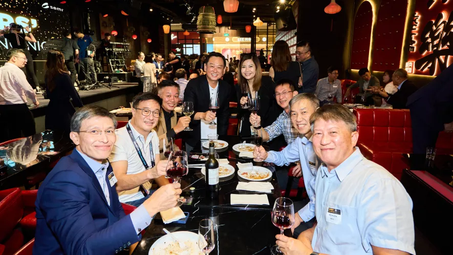
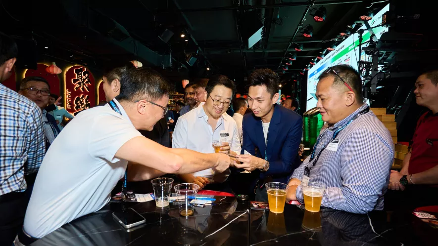
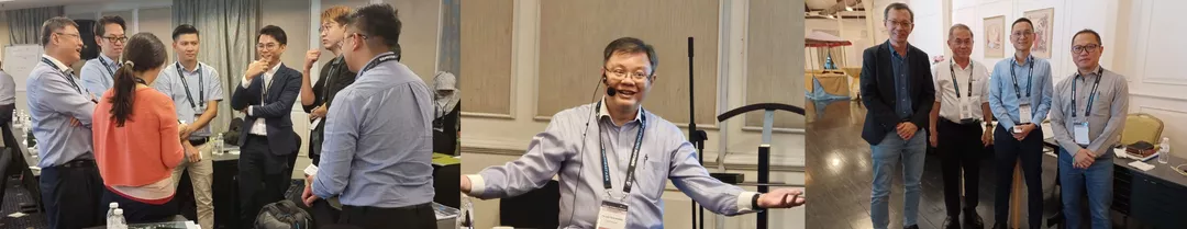
BROWSE OUR PHOTO GALLERY

Penang Business Summit Seminar 1: Advanced Packaging

Royale Chulan Penang
No 1 & 2, Pengkalan Weld, Georgetown
10300 Penang
Pulau Pinang
Malaysia

Image of Dr Lee Teck Kheng
MEET OUR SPEAKER
Dr. Lee Teck Kheng
Director, Technology Development Centre, Institute of Technical Education Singapore,
SEMI SEA Advance Packaging Technical Committee Member
9:00 am

Introduction to IC Packaging & Interconnects

Introduction to IC Packaging
• Functions of Packaging – Mechanical, Material, Electrical and Chemical
• Review of Packaging Trend – BGA, CSP, Fan-in & Fan-out WLP, 3D Packaging, SoC vs SiP etc
• Challenges in Assembly and Packaging

Interconnects
• Overview
• TAB Bonding
• Wirebonding – Ultrasonic, Thermocompression, Thermosonic mechanisms
• Flip Chip Bondings – Thermocompression, C4, Re-cap reflow, solid-state, ACF, Conductive paste bonding

12:00 pm

Lunch

1:00 pm

Board Assembly and Soldering & PCB and IC Carriers

Board Assembly and Soldering
• Through Hole & SMT – Stencil Print Process, Reflow Profile
• Solder Materials – Alloy, Flux, Solvents, self-alignment effect
• Pb Free Solder – Ternary phase diagram, SnAgCu
• Intermetallics and Growth – Diffusion mechanism, Arrhenius equation
• Testing and Reliability – Ball shear & pull failure strength and modes, Fatigue, Weibull distribution

PCB and IC Carriers
• PCB Technology – Material properties, PCB fabrication process, drilling, patterning, plating, solder resist, laminating
• IC Carriers – Design rule, Leadframe, LTCC, Flex and BT substrates
• Substrate Development

4:00 pm

Q&A | Case Studies

5:00 pm

End of Day 1

9:00 am

Assembly Process

• Thickness Reduction – Grinding, Lapping, Polishing, CMP
• Dicing/Singulation – Blade, Laser, Stealth dicing, Dicing after grind
• Die Attach – Eutectic bonding, DA materials, Collets
• Plasma – Argon, Oxygen plasma, Surface tension
• Encapsulation – Mold constitutes and properties, Transfer, Film and compression molding, Dam and fill
• Plating – Solder plating, NiPd finish, PPF
• Trim & Form – ESD, Lead formation, Spring back mechanism

12:00 pm

Lunch

1:00 pm

Material Characterization Techniques

• Introduction
• Bulk Material Characterization – Stress strain, Bending, Impact toughness, TGA, DSC, TMA, DMA
• Interfaces Characterization – Failure mode and strength, Wire pull, Ball pull, Double cantilever bending, Die shear, Mold button shear, Ball shear

2:30 pm

Q&A | Case Studies

3:30 pm

Lucky Draw

3:35 pm

End of Workshop

Note: Program is subject to changes.

Seminar 1 and Seminar 2 timing will overlap on 7 Mar .

- APHI Workforce Development

Advanced Packaging and Material Characterization

*Note: Seminar 1 and Seminar 2 timing will overlap on 7 Mar


Participating Fee:

Usual Member Rate: SGD 750 
Usual Non-member Rate: SGD 935 

*The above rates are inclusive of coffee/tea breaks and luncheon for both days

Register before 23 February 2024 to enjoy Early Bird rate of 15% off the above rates.


A certificate of completion will be awarded at the end of the seminar.


HRD Corp Logo
 

*Malaysian Companies - HRDC Claimable for Penang Business Summit Seminar 1: Advanced Packaging (Advanced Packaging and Material Characterization) (subject to T&C, please contact HRDC for more information).
For HRDC claims, please refer to the following links on the claiming matrix and guidelines:


Contact us for enquiries!

For Program: 

Ms. Cecelia Fong | [email protected] | +65.9750.2382 

For Registration / HRDC Claims: 

Ms. Gillian Lim | [email protected] | +65.9048.1123


Off Add to Calendar 2024-03-06 00:00:00 2024-03-07 00:00:00 Penang Business Summit Seminar 1: Advanced Packaging Advanced Packaging and Material Characterization*Note: Seminar 1 and Seminar 2 timing will overlap on 7 Mar Participating Fee:Usual Member Rate: SGD 750 Usual Non-member Rate: SGD 935 *The above rates are inclusive of coffee/tea breaks and luncheon for both daysRegister before 23 February 2024 to enjoy Early Bird rate of 15% off the above rates. A certificate of completion will be awarded at the end of the seminar.  *Malaysian Companies - HRDC Claimable for Penang Business Summit Seminar 1: Advanced Packaging (Advanced Packaging and Material Characterization) (subject to T&C, please contact HRDC for more information).For HRDC claims, please refer to the following links on the claiming matrix and guidelines:HRDC Approval Letter for Penang Business SummitAllowable Cost MatrixHRDC SBL Grant HelperHRDC SBL Claim Helper Contact us for enquiries!For Program: Ms. Cecelia Fong | [email protected] | +65.9750.2382 For Registration / HRDC Claims: Ms. Gillian Lim | [email protected] | +65.9048.1123  Royale Chulan Penang No 1 & 2, Pengkalan Weld, Georgetown 10300 Penang Pulau Pinang Malaysia SEMI.org [email protected] Asia/Kuala_Lumpur public Asia/Kuala_Lumpur SOLD OUT

Deventer, December 12, 2023 – RoodMicrotec N.V., a leading independent company for semiconductors supply and quality services, and HE System Electronic GmbH, an established development and manufacturing partner for sensors and power electronics, today announce their cooperation to perform certified validation of power modules in the field of electromobility. All qualification and reliability tests will be carried out in compliance with the AQG 324 standard, among others, and the final product will be used in high power solutions such as car batteries. The partnership was initiated in 2021 and is now even stronger with this new project.

The majority of projects at HE System Electronic are located in the automotive sector. In this area, it is important to be certified or accredited according to quality management standards such as VDA 6.2 and DIN EN ISO / IEC 17025:2018.

“RoodMicrotec is one of the few independent service providers in the European region that can carry out a complete validation according to AQG 324. This makes the cooperation with RoodMicrotec so valuable,” says Axel Weber, CEO of HE System Electronic GmbH.

For RoodMicrotec, this partnership fits well into their general range of services and the company is looking forward to realizing further projects in this area, thus planning to expand its capacities.

“The final product from HE System Electronic is highly interesting. Because of this, we have added power cycling to our qualification capabilities. An additional tester with extended high power capabilities has already been ordered, so we can expand our capabilities and provide additional support to our customers,” says Martin Sallenhag, CEO of RoodMicrotec.

About HE System Electronic GmbH
HE System Electronic is a medium-sized electronics and microsystems technology company based in Veitsbronn in the location for business of the metropolitan region Nuremberg. Founded as a provider for electronic manufacturing services in the field of hybrid technology, HE System Electronic is well established as a competent partner for development and manufacturing and has been successful on the market for its customers in the product areas of sensor technology and power electronics for many years. The parent company, TKH Technologie Deutschland AG, based in Bielefeld, is supporting the growth and thus, HE System Electronic offers its customers the best of two worlds: the financially stable background of a healthy and profitable holding company as well as the innovative strength and short distances of a medium-sized company.
For more information please visit he-system.com/en.
Further information
Axel Weber – CEO, Klaus Aßmann – Distribution
Phone +49 911 97 58 10, E-mail: [email protected].

About RoodMicrotec
With more than 50 years of experience in the semiconductor and electronics industry, RoodMicrotec is a leading independent company for semiconductor supply and quality services. RoodMicrotec is a highly valued partner for many companies worldwide and offers specifically tailored turnkey solutions for each single customer's requirements. The turnkey services include project management, wafer test, assembly, final test, qualification, failure analysis, and logistics. All services provided by RoodMicrotec meet the high quality standards of the automotive, industrial, healthcare, and high reliability aerospace sectors. RoodMicrotec is headquartered in Deventer, Netherlands, with operational units in Nördlingen and Stuttgart, Germany.
For more information, please visit https://www.roodmicrotec.com.
Further information
Martin Sallenhag, CEO or Arvid Ladega, CFO
Phone +31 570 745623, E-mail [email protected].

This press release is available in English and German. In case of conflict between these versions, the English version shall prevail.

Registration for this course is free.

For questions, please contact Paul Trio at [email protected]

+
Belgium China France Germany India Ireland Italy Japan Malaysia Russia Singapore South Korea Taiwan United States Vietnam EMS course Ad tile Business Executive

Electromagnetic Interference and Electrical Overstress Management: Why, What, and How

Electromagnetic interference (EMI) is becoming more critical in all aspects of semiconductor manufacturing, affecting productivity and yield.  

The SEMI E176 Standard, "Guide to Assess and Minimize Electromagnetic Interference (EMI) in a Semiconductor Manufacturing Environment," addresses this issue. This document provides practical, actionable guidance on establishing an acceptable EMI environment in semiconductor processes: from assessing the EMI environment to EMI mitigation to verification. SEMI E176 sets recommended EMI limits for different process categories. The Standard can benefit every stage of the semiconductor process and electronic assembly.  
 

Who Should Attend:

  • Semiconductor Device Manufacturers
    • Manufacturing and Quality Directors
    • Department and Production Managers
    • Line Supervisors
    • Sales: VP and Managers
  • Equipment Manufacturers
    • Director-Level and VP Engineering and QA
    • Engineering Department Managers
    • Sales: VP and Managers (customer satisfaction)


Meet the Instructor

Vladimir Kraz


Vladimir Kraz, President, OnFILTER

Biography


SEMI HQ
CA
United States

1. Overview of SEMI and SEMI Standards
- SEMI as a resource for your company

2. EMI and EMC - an overview

3. Effect of EMI on processes and equipment
- EMI and Electrical Overstress
- Equipment precision
- Process variations
- Other problems

4. Sources and propagation of EMI

5. Overview of SEMI E.33
- Emphasis on Table 1: Compliance Assignment/Responsibility Table

6. Overview of SEMI E.176

7. Basics of a viable EMI program at a factory based on SEMI E.176
- Purpose
- Structure
- Resources and budget
- Similarity and synergy with already-existing ESD program

Standards

Join us for a hybrid experience with both in-person and virtual attendance options.

4:00 pm - 5:00 pm Off Add to Calendar 2023-12-18 16:00:00 2023-12-18 17:00:00 EMI and EOS Management Course Join us for a hybrid experience with both in-person and virtual attendance options. SEMI HQ CA United States SEMI.org [email protected] America/Los_Angeles public America/Los_Angeles Register now
Event format

Registration

Registration for this workshop is free.

For questions, please contact Mayura Padmanabhan at [email protected].


+
Belgium China France Germany India Ireland Italy Japan Malaysia Russia Singapore South Korea Taiwan United States Vietnam Cybersecurity workshop new location Business Executive Technical
Highlighted content

SEMI Cybersecurity Launch Workshop

Join us for a 2-day working session to align our industry on concrete next steps to secure semiconductor manufacturing against an ever-evolving threat environment. With our complex and interconnected supply chains, no single company can be safe unless all companies are safe. Our consortium of device makers, foundries, equipment makers, component suppliers, and software suppliers are working together to rapidly develop a practical plan to improve security now, and for years to come while minimizing costs and avoiding duplication.


Who should attend:

• Device makers • Foundries • Tool suppliers • Component makers • Software suppliers ​and CISOs • Executives • Decision-makers • Managers • Security professionals

Intel - SC12 - Santa Clara 12
CA
United States

Day 1: December 6, 2023 - Noon - 7 pm PT

12:00 pm - 7:00 pm

• Consortia governance, structure, deliverables, and roadmap for 2024
• E187 SEMI Standard implementation ideation session
• Develop a method to survey, evaluate, and certify manufacturing equipment cybersecurity protections
• Globalization of SEMI Taiwan’s E187 reference architecture and checklist

Day 2: December 7, 2023 - 8 am - 3 pm PT

8:00 am - 3:00 pm

• Opportunities for collaboration and information sharing for cyber threats and incidents
• Supply Chain Cybersecurity working session
• Create a semiconductor industry-specific framework to measure security and implementation approach across the entire ecosystem
• Review NIST industry profiles and evaluate for suitability in semiconductor
• Next steps: Including forming working groups and assigning leaders

- Standards

Join us for a 2-day workshop aimed at developing and advocating a practical, standards-based, industry-wide approach to improving cybersecurity and resilience across the semiconductor supply chain.

Time:

Day 1: Noon - 7 pm PT

Day 2: 8 am – 3 pm PT

In-person registration has reached capacity. However, you can still register to participate online.


Off Add to Calendar Disabled America/Los_Angeles Register now
Event format
Malaysia TECH TALK OVER COFFEE Banner Business

Supporting Partner

InvestPenang_logo_2022
MSIA_logo_2022
Highlighted content

Macallum Connoisseurs
1, Gat Lebuh Macallum, 10300 George Town, Pulau Pinang, Malaysia
Penang
Malaysia

2:00 pm

Welcome Remarks & Introduction of Speaker

2:15 pm

Navigating Semiconductor Industry in Malaysia: Challenges & Opportunities for Young Engineers

2:45 pm

Dialogue Session

3:15 pm

Networking Tea break

5:00 pm

Program End

Workforce Development

Navigating Semiconductor industry in Malaysia: Challenges & Opportunities for young engineers

This coffee talk session serves as an informal and insightful dialogue for young engineers entering the dynamic semiconductor industry in Malaysia. The discussion focuses on the challenges and opportunities that await them in this vibrant sector. Malaysia's semiconductor landscape is thriving, with numerous multinational corporations contributing significantly to the global supply chain. However, as with any dynamic industry, challenges exist, including staying current with technological advancements, navigating global competition, ensuring quality and reliability, adhering to environmental and regulatory standards, and preparing for potential supply chain disruptions.

Amidst these challenges lies a world of opportunities for young engineers. The semiconductor industry offers an ideal platform for innovation, career growth, global exposure, societal impact, and networking. This session offers valuable recommendations, including embracing lifelong learning, seeking mentorship, building a professional network, cultivating adaptability, finding purpose in work, and maintaining a healthy work-life balance.

The session will emphasize the need to embrace challenges as stepping stones to success while seizing the opportunities to make a meaningful impact in the semiconductor industry. It is an encouragement to the young engineers, assuring them that their talent and determination will leave a significant mark on the industry's landscape.


About Speaker: 

Encik Noorazidi Bin Che Azib

Encik Noorazidi Bin Che Azib

Deputy Vice President, Operation Technology, Strategic Program (OTSP), Inari-Amerton Bhd

Noorazidi (Azidi), a Mechanical Engineering graduate from the University of Nevada, Reno, USA, currently holds the position of Deputy Vice President at INARI, overseeing OTSP (Operation Technology and Strategic Programs) and EHS (Environment, Health, and Safety). Azidi began his career in high-volume semiconductor manufacturing, process engineering, automation system design, Industry 4.0, and environmental sectors, accumulating 35 years of experience at multinational corporations such as AMD, Hewlett Packard, Agilent, and Avago before joining INARI in 2012.

He played a pivotal role in INARI's transformation towards digitalization and the adoption of cyber-physical systems. Known for his passion for innovation and commitment to talent development, he collaborates closely with local academia and industrial skill development centers, helping to prepare over 3,000 interns in the past five years for industry roles.

Azidi's expertise in Industry 4.0 has made him a key figure in collaborations with government agencies, actively supports the development of electrical and electronic supply chains, local small-medium-enterprises (SME) productivity, adoption of advanced technology, and business development. Together with the Group CEO, Mr KC Lau, INARI has also initiated numerous SME development programs under the Inari Waterfall Effect Model, which in line with their Industry 4.0 Roadmap.


Attendee Fees: RM 120 / pax

- Goodie bag, snacks, and drinks are included for session

Contact: [email protected] for any questions


Register Now!

2:00 pm - 5:00 pm Off Add to Calendar 2023-11-30 14:00:00 2023-11-30 17:00:00 Tech Talk Over Coffee | Malaysia, Penang Navigating Semiconductor industry in Malaysia: Challenges & Opportunities for young engineersThis coffee talk session serves as an informal and insightful dialogue for young engineers entering the dynamic semiconductor industry in Malaysia. The discussion focuses on the challenges and opportunities that await them in this vibrant sector. Malaysia's semiconductor landscape is thriving, with numerous multinational corporations contributing significantly to the global supply chain. However, as with any dynamic industry, challenges exist, including staying current with technological advancements, navigating global competition, ensuring quality and reliability, adhering to environmental and regulatory standards, and preparing for potential supply chain disruptions.Amidst these challenges lies a world of opportunities for young engineers. The semiconductor industry offers an ideal platform for innovation, career growth, global exposure, societal impact, and networking. This session offers valuable recommendations, including embracing lifelong learning, seeking mentorship, building a professional network, cultivating adaptability, finding purpose in work, and maintaining a healthy work-life balance.The session will emphasize the need to embrace challenges as stepping stones to success while seizing the opportunities to make a meaningful impact in the semiconductor industry. It is an encouragement to the young engineers, assuring them that their talent and determination will leave a significant mark on the industry's landscape. About Speaker: Encik Noorazidi Bin Che AzibDeputy Vice President, Operation Technology, Strategic Program (OTSP), Inari-Amerton BhdNoorazidi (Azidi), a Mechanical Engineering graduate from the University of Nevada, Reno, USA, currently holds the position of Deputy Vice President at INARI, overseeing OTSP (Operation Technology and Strategic Programs) and EHS (Environment, Health, and Safety). Azidi began his career in high-volume semiconductor manufacturing, process engineering, automation system design, Industry 4.0, and environmental sectors, accumulating 35 years of experience at multinational corporations such as AMD, Hewlett Packard, Agilent, and Avago before joining INARI in 2012.He played a pivotal role in INARI's transformation towards digitalization and the adoption of cyber-physical systems. Known for his passion for innovation and commitment to talent development, he collaborates closely with local academia and industrial skill development centers, helping to prepare over 3,000 interns in the past five years for industry roles.Azidi's expertise in Industry 4.0 has made him a key figure in collaborations with government agencies, actively supports the development of electrical and electronic supply chains, local small-medium-enterprises (SME) productivity, adoption of advanced technology, and business development. Together with the Group CEO, Mr KC Lau, INARI has also initiated numerous SME development programs under the Inari Waterfall Effect Model, which in line with their Industry 4.0 Roadmap. Attendee Fees: RM 120 / pax- Goodie bag, snacks, and drinks are included for sessionContact: [email protected] for any questions Register Now! Macallum Connoisseurs 1, Gat Lebuh Macallum, 10300 George Town, Pulau Pinang, Malaysia Penang Malaysia SEMI.org [email protected] Asia/Kuala_Lumpur public Asia/Kuala_Lumpur SIGN UP

Trading Update: RoodMicrotec announces total income for the third quarter of 2023

• Total income for the third quarter of 2023 was EUR 4.2 million (2022: EUR 4.3 million)
• Total income for the first nine months of 2023 was EUR 12.9 million (2022: EUR 11.7 million)
• Order book value increased compared to the beginning of the quarter

Deventer, October 19, 2023 – RoodMicrotec N.V., a leading independent company for semiconductors supply and quality services, today releases its trading update for the third quarter of 2023. The total income for the third quarter of 2023 was EUR 4.2 million, marginally lower than in the third quarter of 2022 (EUR 4.3 million). The total income for the first nine months of 2023 was EUR 12.9 million, an increase of 10% compared to the same period in 2022 (EUR 11.7 million). The good start in the first quarter of this year and the stable development in the second and third quarters are the base for this increase.
The order book increased compared to the beginning of the quarter and continues to be filled with long-term contracts and engagements as well as short-term orders. The long-term contracts and engagements are mainly in the SCM and Test Operations units and the short-term orders in the Failure Analysis & Qualification unit.
“It is encouraging to see that the total income for the first nine months is higher than for the same period last year even though the market situation with high inflation and rising interest rates is getting worse. We continue to support our customers with high quality services and they highly appreciate it.”, says Martin Sallenhag, CEO of RoodMicrotec. “The steady increase in the order book value is building a good foundation for our future business.”

Outlook
RoodMicrotec expects the total income for 2023 to be in the range of EUR 17.0 million to EUR 17.5 million, with a profit before tax ratio from 5 to 10% of total income, excluding the advisory expenses incurred for the public offering process. This projection is in line with the financial targets communicated to the financial market previously. The geopolitical situation in the world and the trends with higher inflation, rising prices, and increasing interest rates throughout Europe could have an impact on the Company’s business. The Management is keeping a close eye on the situation and is doing everything possible to mitigate any potentially negative impact.

Audit
The financial data in this press release have not been audited.

Today’s Extraordinary Meeting of Shareholders
RoodMicrotec will hold an Extraordinary Meeting of Shareholders at Amsterdam Stock Exchange (Euronext), Beursplein 5, 1012 JW in Amsterdam, the Netherlands, this afternoon starting at 14:00 CEST in relation to the recommended public offer by Microtest S.p.A. for all the issued and outstanding ordinary shares in the capital of RoodMicrotec N.V.

About RoodMicrotec
RoodMicrotec is a leading independent company for semiconductor supply and quality services. With more than 50 years of experience in the semiconductor and electronics industry, RoodMicrotec is well-established as a highly valued partner for many companies worldwide. The Company provides full-turnkey ASIC services for complex microchips that are customized to handle specific applications for individual customers. In cooperation with strong partners, RoodMicrotec manages the entire development and production flow of ASICs in the target volume, ranging from low quantities up to multiple millions per year. The turnkey solution includes project management, wafer test, assembly, final test, qualification, failure analysis and logistics. All services comply with the industrial and quality requirements of the high reliability, aerospace, automotive, healthcare and industrial sectors. RoodMicrotec’s headquarters are located in Deventer, Netherlands, with operational units in Nördlingen and Stuttgart, Germany
For more information visit https://www.roodmicrotec.com

This press release is published in English and German. In case of conflict between these versions the English version shall prevail. This communication contains information that qualifies as inside information within the meaning of Article 7(1) of the EU Market Abuse Regulation. The company’s managing director and CEO Martin Sallenhag, is responsible for arranging the release of this document on behalf of RoodMicrotec.

Deventer, October 12, 2023 – RoodMicrotec N.V., a leading independent company for semiconductors supply and quality services, and CERN, the European Laboratory for Particle Physics, are expanding their collaboration with the Compact Muon Solenoid (CMS) Outer Tracker ASICs project. The long-standing partners are thus jointly facing another large and significant project.

The ASICs tested for the CMS will enable the collection of essential data during experiments in the Large Hadron Collider (LHC). The LHC is purpose-built to help scientists in addressing fundamental questions within the field of particle physics.
As part of the planned 2026 upgrade to the CMS detector, CERN will again use RoodMicrotec's expertise and testing services. RoodMicrotec will test and deliver over 1,000 12" silicon wafers. The three ASIC modules on the wafers will become an integral part of the detectors. They will collect and process the enormous amounts of data that emerge during the generation of collision experiments.

"We are very pleased to have this long-standing partnership with RoodMicrotec. In the past, we have been able to successfully test and apply the ASIC components that are so important for science," says Kostas Kloukinas, project manager of the CMS Outer Tracker ASICs project at CERN.

For RoodMicrotec, the cooperation with CERN also means a lot. Especially the opportunity to contribute to the progress of science is very fascinating. Furthermore, the project helps to advance the company's own expertise even further.

"The employees of RoodMicrotec are proud to be able to significantly contribute with their services to the basic research of the large CERN family," says Martin Sallenhag, CEO of RoodMicrotec.

About CERN
CERN, the European Laboratory for Particle Physics was founded in 1954 and is the world's leading laboratory for particle physics. Here, physicists and engineers explore the fundamental structure of the universe to find out what it is made of and how it works. For their studies of the basic constituents of matter – the elementary particles – they use the world’s largest and most complex scientific instruments. To investigate those particles, they are accelerated to almost the speed of light and thus made to collide. The resulting events tells physicists how particles interact and provide insights into fundamental laws of nature. CERN has 23 member states and further nations from all over the world that contribute to its research programs.
For more information please visit https://home.cern/science/experiments/cms

About RoodMicrotec
With more than 50 years of experience in the semiconductor and electronics industry, RoodMicrotec is a leading independent company for semiconductor supply and quality services. RoodMicrotec is a highly valued partner for many companies worldwide and offers specifically tailored turnkey solutions for each single customer's requirements. The turnkey services include project management, wafer test, assembly, final test, qualification, failure analysis, and logistics. All services provided by RoodMicrotec meet the high quality standards of the automotive, industrial, healthcare, and high reliability aerospace sectors. RoodMicrotec is headquartered in Deventer, Netherlands, with operational units in Nördlingen and Stuttgart, Germany.
For more information, please visit https://www.roodmicrotec.com

This press release is available in English and German. In case of conflict between these versions, the English version shall prevail.

Malaysia Singapore Vietnam Members' Networking Night Business Executive
Highlighted content

Photo Gallery

Browse our 2024 Singapore Members' Networking Night Photo Gallery

Jyu Lae Bistro @ Suntec Tower 5
3 Temasek Blvd, #01-315
Singapore 038983
Singapore

6:00 pm

Registration & Cocktail Reception

6:30 pm

Live Performance I

6:40 pm
Andrew_Goh_SEA
Mr. Andrew Goh

Welcome Speech

Mr. Andrew Goh | Vice Chairman, SEMI Southeast Asia Regional Advisory Board | Corporate Vice President and General Manager, Southeast Asia Lam Research Singapore

7:00 pm

Networking Buffet & Drinks

9:15 pm

Live Performance II

10:00 pm

End of Networking Night

Program is subject to change

Join SEMI Southeast Asia for a night of networking and celebration at our exclusive Members' Networking Night. Get a chance to connect with other industry leaders, exchange valuable insight on the sector, and unlock a myriad of business opportunities.


Non-member fee: SGD 800 (limited tickets available)

Members: Free (restricted to 2 pax per member company)

Time

6:00 pm - 9:30 pm

Location

Jyu Lae Bistro @ Suntec Tower 5
3 Temasek Blvd, #01-315
Singapore 038983
Singapore

Direction to Jyu Lae Bistro

 Jyu Lae

Contact us for enquiries!

For the event:

Mr. Glenn Tan | [email protected] | +65.8228.0662

For registration:

Ms. Gillian Lim | [email protected] | +65.9048.1123

6:00 pm - 9:30 pm Off Add to Calendar 2024-10-10 18:00:00 2024-10-10 21:30:00 Members' Networking Night Join SEMI Southeast Asia for a night of networking and celebration at our exclusive Members' Networking Night. Get a chance to connect with other industry leaders, exchange valuable insight on the sector, and unlock a myriad of business opportunities. Non-member fee: SGD 800 (limited tickets available)Members: Free (restricted to 2 pax per member company)Time6:00 pm - 9:30 pmLocationJyu Lae Bistro @ Suntec Tower 53 Temasek Blvd, #01-315Singapore 038983SingaporeDirection to Jyu Lae BistroContact us for enquiries!For the event:Mr. Glenn Tan | [email protected] | +65.8228.0662For registration:Ms. Gillian Lim | [email protected] | +65.9048.1123 Jyu Lae Bistro @ Suntec Tower 5 3 Temasek Blvd, #01-315 Singapore 038983 Singapore SEMI.org [email protected] Asia/Singapore public Asia/Singapore

PENANG, MALAYSIA - OCTOBER 2023 Curious about how Integrated Circuit (IC) manufacturers keep pace with fast-changing technology? Discover how automated systems are revolutionising the semiconductor industry, enhancing production efficiency and cost-effectiveness.

ViTrox, which aims to be the world’s most trusted technology company, is thrilled to introduce a game-changing addition to our advanced machine vision inspection solutions: the 4-sided Auxiliary (AUX 4S+) Inspection Module. This exciting optional add-on feature is designed with our customers' needs in mind and is set to elevate the capabilities of Tray-to-Tray Vision Inspection Handler – TH3000i and Tray-to-Tape & Reel Vision Inspection Handler – TR3000i.

Our Tray-Based Vision Handlers, the TH3000i and the TR3000i are high-quality machine vision inspection solutions that support emerging industries like 5G, IoT, Automotive, and Industry 4.0, with the main difference being their handling mechanism. Both tray-based handlers are designed to support inspection capabilities that accommodate IC package sizes up to 120 mm x 120 mm, including BGA, QFP, QFN, CSP, TSSOP, MSOP, and SOP. In addition, both solutions offer an array of benefits, such as high-speed IC inspection, easy operation, quick conversion time, and low maintenance cost.

The auxiliary module inspection function enables more precise defect detection that occurs at the sides of the semiconductor device. This is achieved via dedicated optics, lighting and software algorithms. The optional advance inspection function is particularly beneficial for customers who demand stringent product quality, especially for automotive, computing, and telecommunications end-applications.

The AUX 4S+ elevates electronics manufacturing to the next level by providing a comprehensive 4-sided inspection solution. It's all about ensuring the highest quality and reliability of customers’ electronic components. Explore the awe-inspiring capabilities of the AUX 4S+ showcased below.:

Enhanced Inspection Capabilities
The AUX 4S+, built upon an innovative design concept, goes beyond conventional inspection capabilities. In addition to the bottom and side vision station, it features an additional vision module dedicated to performing direct side view inspections on specialised devices like Power Devices, Land Grid Array (LGA), and Ball Grid Array (BGA) with Metal Lid components. This advanced hardware concept incorporates high-performance cameras, precision lighting, and motorised focusing mechanisms, ensuring adaptability across a wide range of package sizes. Furthermore, its cutting-edge software concept employs advanced algorithms tailored for intricate inspections. As a result, the AUX 4S+ significantly enhances inspection capabilities, meticulously inspecting products from all angles, reducing the risk of unnoticed defects, and ultimately upholding the highest standards of quality and reliability.

Seamless Integration
Designed for seamless integration with your TH3000i and TR3000i models, the AUX 4S+ offers vision-enabled flexibility and ease of use in inspection processes. This integration streamlines workflow by harnessing the power of advanced vision technology. It reduces downtime and minimises manual intervention, resulting in faster and more efficient inspections. This vision-enabled workflow optimisation allows users to meet production schedules, reduce operational costs, and deliver products to customers with uncompromised quality.

Comprehensive Inspection Coverage
The existing TH3000i and TR3000i solutions offer 3D vision inspection, Leaded Packages Inspection, Ball Packages Inspection, Leadless Packages Inspection, Top 3D POP Inspection, 2D Barcode Inspection, Mark Inspection, Package Vision Inspection, Passive Component Inspection, and 6-sided (6S) Colour Inspection. By adding the AUX 4S+ vision inspection module, users can now comprehensively cover a wide range of inspection items, including side package defects, Lid Gap inspection, Package Height inspection, and more. With the advanced vision capabilities to ensure meticulous inspection of every detail, users can save initial costs of investments as they can now rely on one solution for various inspections.

Versatile Package Size and Thickness Support
Another significant advantage of the AUX 4S+ vision inspection module is its versatility when it comes to accommodating component sizes. From compact 2x2 mm to spacious 120x120 mm packages, the system seamlessly adapts with minimal need for conversion kits. Additionally, it offers automated conversion, effortlessly transitioning between these diverse package sizes. This not only simplifies users’ inspection operations but also minimises the need for costly specialised equipment. As a result, it improves production efficiency and keeps the operational cost to a minimum.

At ViTrox, we are dedicated to empowering users with cutting-edge solutions to enhance product quality and manufacturing efficiency. The AUX 4S+ is the latest testament to our commitment to innovation and excellence; it's a game-changer for electronics manufacturing processes.

Are you interested in learning how to further enhance your IC package inspection for better results? Get in touch with us at [email protected] to learn more about our impressive AUX 4S+ feature and master the art of automation!

About ViTrox Technologies
ViTrox is committed to being the World’s Most Trusted Technology Company and the leading solutions provider through the most innovative, advanced, and cost-effective machine vision solution of excellent quality to its customers by integrating ViTrox’s technologies, people, and strategic alliances.

ViTrox offers a full spectrum of solutions, ranging from Middle & Back-end Semiconductor Inspection Solutions, SMT PCB Assembly Vision Inspection Solutions, Integrated Industrial Embedded Solutions, and Industry 4.0 Manufacturing Intelligence Solutions. ViTrox is headquartered in Penang, Malaysia, with offices in Asia, Germany, and the United States and sales and support sites worldwide.

For more information about ViTrox’s products and services, please visit www.vitrox.com.

Deventer, September 28, 2023 – RoodMicrotec N.V., a leading independent company for semiconductor supply and quality services, and Angst+Pfister Sensors and Power AG, an independently operating company of the Angst+Pfister Group, today announce their cooperation for testing semiconductor-based temperature sensors. These highly accurate sensors are able to measure extremely fine temperature differences down to +/-0.1 °C in wide temperature ranges from -45 °C to 130 °C.

Such sensitive and particularly accurate sensors will subsequently be used in industrial applications, in medical technology, and in the automotive sector and thus have to be tested with the greatest precision. In addition, these sensors have a very small drift, a repetition accuracy of 0.01 °C and a extremely fast reaction speed. Another advantage is that the sensor can be customized. The housing, the sensor technology, or the cables can be specially adapted to customer requirements.

"For this project, it was important for us to have a reliable partner who works with the utmost care. As our high-quality components are often used in very sensitive areas, they need to be tested at the highest level," says Robin Ellinger, Product Manager Temperature Sensors of Angst+Pfister Sensors and Power.

For RoodMicrotec, this collaboration means a great appreciation of its capabilities, as the company specializes in the precise testing of highly sensitive components.

"We are really pleased that the quality of our work and our capabilities are so highly appreciated in the semiconductor business. For us, the most fundamental basis of a strong cooperation is mutual trust," says Martin Sallenhag, CEO of RoodMicrotec.
About Angst+Pfister Sensors and Power AG

About Angst+Pfister
Angst+Pfister Sensors and Power AG belongs to the Angst+Pfister Group. The Group´s headquarter is located in Switzerland. It has been a leading developer and manufacturer of technical components and engineering solutions for more than 100 years. With local sales and technical support units as well as logistics centers all over the world, the company serves more than 20,000 customers of numerous industries in over 50 countries. Angst+Pfister operates state-of-the-art research and development centers in Switzerland, Turkey, and Italy. Furthermore, the company runs its own production facilities for elastomer and rubber-metal parts and compounds in Switzerland, Turkey, Italy, Denmark, China, and Vietnam. To complement the capabilities, Angst+Pfister has production partners in over 15 countries, thus enabling the Group to always be at the cutting edge of technology.

Angst+Pfister attaches the utmost importance to reliability and flexibility as well as the respectful and fair treatment of all people who are somehow correlated with them. In proactively implementing the principles of the "United Nations Global Compact", Angst+Pfister pursues the goal of sustainability in all its activities in order to have a positive impact on our planet and society through pragmatic, meaningful, and measurable initiatives.

For more information please visit www.sensorsandpower.angst-pfister.com

About RoodMicrotec
With more than 50 years of experience in the semiconductor and electronics industry, RoodMicrotec is a leading independent company for semiconductor supply and quality services. RoodMicrotec is a highly valued partner for many companies worldwide and offers specifically tailored turnkey solutions for each single customer's requirements. The turnkey services include project management, wafer test, assembly, final test, qualification, failure analysis, and logistics. All services provided by RoodMicrotec meet the high quality standards of the automotive, industrial, healthcare, and high reliability aerospace sectors. RoodMicrotec is headquartered in Deventer, Netherlands, with operational units in Nördlingen and Stuttgart, Germany.
For more information, please visit https://www.roodmicrotec.com

This press release is available in English and German. In case of conflict between these versions, the English version shall prevail.