downloadGroupGroupnoun_press release_995423_000000 copyGroupnoun_Feed_96767_000000Group 19noun_pictures_1817522_000000Member company iconResource item iconStore item iconGroup 19Group 19noun_Photo_2085192_000000 Copynoun_presentation_2096081_000000Group 19Group Copy 7noun_webinar_692730_000000Path
Skip to main content
Default Banner Image

Malaysia

Penang, Malaysia – May 2025 – ViTrox, which aims to be the World’s Most Trusted Technology Company, is proud to announce its participation in SEMICON Southeast Asia 2025, taking place from 20 to 22 May 2025 at the Sands Expo and Convention Centre, Singapore, at Level 1, Booth #L2201. This year marks a significant milestone as ViTrox celebrates its 25th Anniversary, commemorating a quarter-century of innovation and technological breakthroughs in the semiconductor and electronics industries.

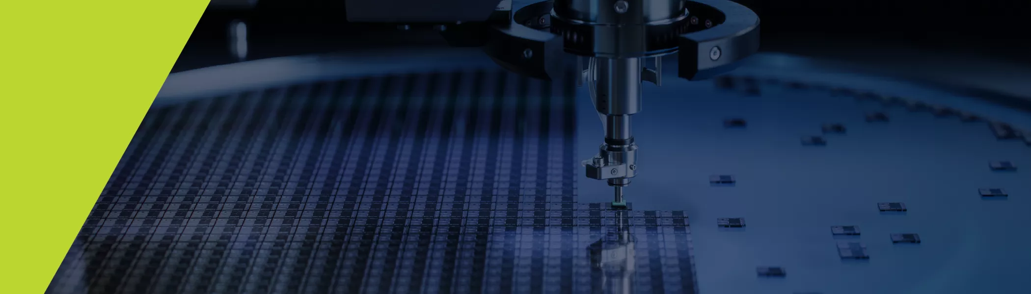
SEMICON SEA serves as a premier platform that unites industry decision-makers, showcases cutting-edge products, and presents the latest market and technology trends. As a global leader in vision inspection solutions, ViTrox will unveil its comprehensive range of next-generation innovations, including Middle & Back-end Semiconductor Vision Solutions, SMT PCB Assembly Vision Solutions, Integrated Industrial Embedded Solutions, and Manufacturing Intelligence Solutions Towards Industry 5.0, demonstrating ViTrox’s ongoing commitment to smarter, more efficient, and high-quality manufacturing.

Key breakthroughs:

PX40i Die Sorting, Inspection & Package Solution: An advanced, fully integrated solution designed to streamline and enhance the semiconductor back-end process through high-precision die sorting, six-sided automated optical inspection, and packaging over a wide range of packaging types.

TH3000i Tray-based Vision Handler: Integrates Artificial Intelligence (AI) for next-level semiconductor inspection. The advanced SWIR inspection technology detects microcracks and internal defects with exceptional accuracy, while 4-side direct inspection ensures total quality control. Beyond inspection, the TH3000i is also built for factory automation to help manufacturers minimise manual intervention, optimise workflow, and move closer to a lights-off factory vision.

V510i 3D AOI for Advanced Packaging (Semicon AOI & Micro AOI): An AI-powered solution with advanced 3D optical inspection of wire bonds, die defects, and solder bumps, offering up to 50% yield improvement while significantly reducing operating costs.

Beyond inspection systems, ViTrox will also showcase its powerful Manufacturing Intelligence Solutions Towards Industry 5.0 - V-ONE. This smart manufacturing platform optimises production efficiency through real-time data visualisation, AI-driven insights, and full traceability.

Integrated Industrial Embedded Solutions, designed to strengthen the automation foundation of production lines through a wide range of advanced offerings, including EtherCAT based I/O Solutions, Illumination Systems, and Motion Solutions.

VisionXpert Smart Code Reader (XS Series): A high-performance smart code reader designed to enhance traceability and productivity through advanced decoding, deep learning, and AI auto-tuning.

VisionXpert Smart Camera (XC Series): A compact yet powerful "mini AOI" solution that integrates advanced vision tools, AI auto-tuning, and deep learning to deliver highly accurate inspection results.

Never let technical obstacles hold you back! Our ViTrox specialists will be on-site to answer your questions and provide live product demos. To experience our solutions firsthand, schedule an appointment by clicking this link or scanning the QR code below.

Contact us via [email protected] for more information. We look forward to welcoming you at SEMICON SEA 2025!

About ViTrox Technologies
ViTrox is committed to being the World’s Most Trusted Technology Company and the leading solutions provider by integrating ViTrox's technologies, people, and strategic alliances to provide its customers with the most innovative, advanced, and cost-effective machine vision solutions of excellent quality.

ViTrox offers a full spectrum of solutions, ranging from Middle & Back-end Semiconductor Inspection Solutions, SMT PCB Assembly Vision Inspection Solutions, Integrated Industrial Embedded Solutions, and Manufacturing Intelligence Solutions Towards Industry 5.0. ViTrox is headquartered in Penang, Malaysia, with offices in Asia, Germany, and the United States and sales and support sites worldwide.

For more information about ViTrox’s products and services, please visit www.vitrox.com.

[March 26, 2025 – Singapore] Test Research, Inc. (TRI), the leading test and inspection systems provider for the electronics manufacturing industry, will join SEMICON SEA held at the SANDS Expo and Convention Centre in Singapore from May 20 - 22, 2025. Visit booth #L2632 to learn about AI-powered AOI solutions for Advanced WLP/PLP and SEMI Back-End Package processes.

TRI will be exhibiting the new Wafer Inspection Platform, TR7950Q SII, featuring a High-resolution 2.5 μm 25MP camera and the TSV Metrology Module. The TR7950Q SII can perform Wafer Macroscopic 3D Inspection and micro measurement metrology. The TR7950Q SII can inspect Advanced WLP, Wafer Frame, Patterned Wafer, Wafer Bumping, WLCSP, through-silicon via (TSV), and more. The TR7950Q SII can measure TSV at ultra-high speeds, measuring sensing TSV depth, trench depth, oxide, nitride, PR, and PI film thickness.

Additionally, TRI will showcase the TR7007Q SII-S, the high-accuracy 3D SEMI SPI for precise solder measurements, supporting applications such as Mini-LED, C4 bumps (~100 μm Ø), and 008004 paste inspection. The lineup will also feature an X-ray Inspection Demo Station.

Join us at booth #L2632 at SEMICON SEA 2025 to discover TRI's cutting-edge SEMI inspection and metrology solutions!

Invitations and Registration

REGISTRATION FOR GCSW is CLOSED.  

All sessions are free of charge to Semiconductor Climate Consortium (SCC) and Energy Collaborative (EC) members.  Others will be admitted by invitation on a case-by-case basis.  Multiple attendees (up to 3) from your company are welcome, but must be invited. Exceptions can be made to the 3 persons limit to have the RIGHT people, with direct responsibility for subjects being discussed.

Belgium China France Germany Ireland Italy Japan Malaysia Singapore South Korea Taiwan United States Vietnam Interested in Attending? Business Executive Expositions
SEMI Logo Social Media
Logo_SQ_Google
scc logo
Highlighted content

Objective of GCS Workshops

A gathering of the semiconductor value chain in one place to most efficiently share solutions and tools and workshop solutions, thereby optimizing your time and resources dedicated to addressing the specific challenges we face. The GCS Workshops are co-hosted by SEMI, the Semiconductor Climate Consortium, Apple, and Google. 

The Workshops are focused on revealing the right details and data that will support action on decarbonization recommendations. The Workshops will NOT focus solely on the issue and roadblocks, but rather the solutions, including (1) sharing examples of successful paths, (2) provide possible tools you need to help address the gaps, and (3) active workshopping on further solution spacing towards emission reductions. We have identified leaders with the experience and knowledge to move toward answers during each Workshop. 

Bring your experience, critical thinking skills, and share with your fellow sustainability travelers.

Workshop Themes and Layout

5/15 – Opening + Facilities Abatement Tours (Tours are now full)

5/16 (AM) - Manufacturing Scope 1 Emissions – brownfield abatement retrofits, low GWP gas substitution and emission measurements reduction solutions, toolkits, roadblocks

5/16 (PM) - Manufacturing Energy Efficiency – fab/subfab interoperability, toolkits and ROI calculations

5/19 (AM) - Renewable Energy Education & Advocacy – global state-of-play, market breakouts for education and solution short listing

5/19 (PM) - Manufacturing Scope 3 Materials Decarbonization – partner paths, impacts and tools

5/20 (AM) - Data & Reporting Alignment – ROI and roadblocks + Closing (PM)

Synergies with the Semiconductor Climate Consortium 

Many themes of the GCS Workshops are outcomes of the discoveries in the SCC Working Groups and previous Supplier Day presentations.  The GCS Workshops will allow for greater depth of discussions and face-to-face solutioning opportunities.  With the right information and the right audience, attendees will depart with tools to operationalize for action.  Across the ecosystem, we want to see those benefits show up in our Scope 3 calculations. 

Microsoft Offices & Sands Convention Center
Singapore
Singapore

12:00 pm - 1:00 pm

Registration & Networking Lunch

Meet and connect with key industry stakeholders, policy leaders, and Microsoft’s sustainability leadership.

1:00 pm - 1:10 pm
Mousumi Bhat
Mousumi Bhat, PhD
VP SEMI Sustainability
SEMI

SEMI Global Climate Summit Workshops: Welcome

1:10 pm - 1:25 pm
Giorgio Fortunato
Giorgio Fortunato
Google

Energy in the APAC Region: Outlook & Strategies

1:30 pm - 1:45 am
susannah calvin
Susannah Calvin
Environment & Supply Chain Innovation
Apple, Inc.

Journey to Carbon Neutral - Supply Chain Focus

1:45 pm - 2:05 pm
Leslie Esparza
Leslie Esparza
Director, Responsible Sourcing
Microsoft
Leo Aspauza
Microsoft
William Hudson
Moderator
Will Hudson
Microsoft

Reflections on Microsoft Supplier Days & Looking Forward

2:05 pm - 2:15 pm
Mousumi Bhat
Mousumi Bhat, PhD
VP, Global Sustainability
SEMI

Overview of GCSW Workshops

2:15 pm - 6:30 pm

Facilities Abatement Tours

(Tours are full and no longer available to new registrants.)

Workshop 1: Manufacturing Fab Scope 1 Emissions

8:30 am - 8:50 am

Breakfast and Networking

8:50 am - 9:20 am
Beth Elroy
Beth Elroy
Vice President, Global EHS & Sustainability
Micron

Collaborative solutions for emissions challenges

9:20 am - 9:35 am
Cristal Phwan
Cristal Phwan
APAC Sustainability Team Manager
GlobalFoundries

Fabs Deploying new abatement tech; brownfield retrofits

9:35 am - 9:50 am
Robin Sim
Robin Sim
Facility Manager - Operation & Hookup Program
STMicroelectronics

Innovative ways to complete brownfield retrofits while minimizing fab disruption

9:50 am - 10:05 am
Hak Joon Kim
Dr. Hak Joon Kim
Principal Researcher
Korea Institute of Machinery and Materials (KIMM)

New abatement tech for both greenfield & brownfield fabs

10:05 am - 10:20 am
Haein Cho
Dr. Haein Cho
Samsung

Samsung's journey to net zero & Scope 1 strategies

10:20 am - 10:45 am

Workshop 1

- Retrofits: Learnings; forward-looking; benchmark projects; modular approaches
- Abatement Technology / Performance Roadmap: accelerating timelines; trends; alignment

10:45 am - 11:15 am
Scott Clendenning
Scott Clendenning, PhD
Intel
Gottfried Wastlbauer
Dr. Gottfried Wastlbauer
Head of Positioning & Business Model
Electronics business of Merck KGaA, Darmstadt, Germany

Low GWP Gases

11:15 am - 11:40 am

Workshop 2: Risk assessment & Methodology

11:40 am - 12:40 pm
Dr. Shou Nam Lee
Dr. Shou-Nan Li
ITRI
Rahul Singh
Dr. Rahul Singh
Manager, Emissions Analysis
Micron
Troy Boley
Troy Boley
President
Spectrum
Jonghan Lee
Jonghan Lee
SK Hynix

Emissions Measurement

12:40 pm - 1:05 pm

Workshop 3: Real-time monitoring, calibration variation, regulatory

1:05 pm - 1:30 pm

Readouts & Lunch Break

Workshop 2: Manufacturing Energy Efficiency – fab/subfab interoperability, toolkits and ROI calculations

1:30 pm - 2:00 pm
Kevin Chan
Kevin Chan
Lead, Artificial Intelligence
Micron

IDM perspective, state of the art sensor deployment & best practices for energy efficiency

2:00 pm - 2:15 pm
James Oh
James Oh
Aveva

Immediate Opportunities around Energy Efficiency

2:15 pm - 2:30 pm
John Golightly
John Golightly
VP of Sustainability
ASM

ASM Energy Efficiency Story

Net Zero Operations through Innovation and Collaboration

2:30 pm - 3:00 pm

EE Workshop 1: Sensor Deployment for Equipment

From energy sensor to harmonics & power quality detection and remediation

3:00 pm - 3:45 pm
Shaun Crawford
Shaun Crawford
Product Manager
Applied Materials
Stefanie Hammer
Stefanie Hammer
General Manager
Algorismic
Michael Neel
Michael Neel
Director of Marketing
Inficon

Operations Energy Efficiency Opportunities, Process and Recommendations

State-of-the-art Sub-Fab Interoperability

3:45 pm - 4:15 pm
TBD

EE Workshop 2: Communication & Interoperability

4:15 pm - 4:45 pm
Slava Libman
Slava Libman
FTD Solutions
James Oh
James Oh
Aveva
Mark da Silva
Mark da Silva
SEMI Smart Manufacturing

Current Solutions - Data Aggregation & Dashboard: Case Study

4:45 pm - 5:15 pm
Teh Seimens
Teh Tiack Ein
Head of Presales, Southeast Asia
Siemens Digital Industries Software
Arul
Arul Ambikapathi
Lam Research
Mark da Silva
SEMI Smart Data AI Initiative

Future Solution - Digital Twin (Design, Build, Operate & Maintain a Fab)

5:15 pm - 5:45 pm

Workshop 3: Data Management & Reporting

5:45 pm - 6:00 pm

Read out

Workshop 3: Renewable Energy Education & Advocacy – global state-of-play, market breakouts for education and solution short listing

8:00 am - 8:30 am

Networking & Breakfast

8:30 am - 9:00 am
Low - EMA
Xin Wei Low
Assistant Chief Executive
EMA

The Net Zero Imperative and Singapore's Role

9:00 am - 9:20 am
William Hudson
Will Hudson
Asia Pacific Sustainability Policy Director
Microsoft

One Goal, One Grid; Unlocking Clean Power Together

9:20 am - 9:50 am
Ali Izadi
Ali Izadi-Najafabadi
Head of APAC
Bloomberg NEF

Global state of play on accessible RE

9:50 am - 10:10 am
Michael Thomas
Mike Thomas
Managing Director
Lantau Group

Friendly Policies to Renewable Energy

10:10 am - 10:20 am
Eric Gibbs
Clean Energy Buyers Association

Procurement Hub

10:30 am - 12:00 pm

Breakouts/Workshop: RE Education & Awareness

Two parallel sessions will be held.
Group A - Room 3111: South Korea (45 min) and Japan (45 min)
Group B - Room 3112: Singapore/Malaysia (45 min) and Taiwan (45 min)

10:30 am - 11:15 pm
Seiya Miyake
Seiya Miyake
Renewable Energy Promoting Organization, Inc.
Shawn Woo
3 Degrees

How to Procure: Japan

11:15 am - 12:00 pm
Oursan Jin
Ousam Jin
CREF

How to Procure: South Korea

10:30 am - 11:15 am
Henry Eu
Asia Clean Energy Consortium (ACEC)
Greg Thomassin
Gregory Thomassin
Business Development
Total Energies
Michael Thomas
Mike Thomas
LTG

How to Procure: Singapore/Malaysia

11:15 am - 12:00 pm
Jung Choi
Jung Choi
Regional Manager for Asia-Pacific
CRS
Wei In
Wei-In Lin
Apala

How to Procure: Taiwan

12:00 pm - 12:15 pm

Workshop Readout

12:30 pm - 1:00 pm
Albert Sutaru
Albert Sutanto
Manager SE Asia Markets and Global EACs Sourcin
Mt. Stonegate

Achieving 100% RE in Asia: Market Highlights and Corporate Sourcing

(a working lunch)

1:00 pm - 1:20 pm
Robbert Slooten
Robbert Slooten
Manager, Renewable Energy and Carbon Advisory
Schneider Electric
Bess Ng
Bess Ng
Associate Principle, Sustainability Business
Schneider Electric

How to leverage the power of buyers’ groups for renewable electricity adoption in key markets - Korea, Singapore, and Japan

(a working lunch)

Workshop 4: Manufacturing Scope 3 Materials Decarbonization – partner paths, impacts and tools

1:30 pm - 1:50 pm
Han Chen
Han Chen
Asia Clean Energy Policy
Apple

The importance of scope 3 for Apple and the Path Forward Together

1:50 pm - 2:20 pm
Sebastian Goke, McKinsey & Company
Sebastian Goeke
Associate Partner
McKinsey & Company

Gaining transparency on Fab Scope 3 upstream emissions

2:20 pm - 2:50 pm
Christof Witte
Christof Witte
Partner
McKinsey & Company

How to drive upstream FAB decarbonization

2:50 pm - 3:10 pm
Stehanie Cotton
Stephanie Cottin
Sustainability and Safety Director & Chief of Staff to COO
Soitec

Examples of upstream suppliers taking accountability, decarbonizing

3:10 pm - 3:40 pm
Frank Bartels
Frank Bartels
Director Global Marketing and Product Management, Semiconductor Materials
BASF

Smart decarbonization of wet process solutions

3:40 pm - 4:00 pm
Corinna Wolf
Corinna Wolf
Head of Global Sustainability
Infineon

How to hold your supply chain accountable, educate them on decarbonization, and implement solutions

4:00 pm - 4:15 pm
Handy Ko
Handy Ko
Director of Materials Management
TSMC

Responsible Supply Chain Management

4:15 pm - 4:35 pm
Photo of Speaker Jordan Davis blond hair brown eyes
Jordan Davis
Responsible Business Alliance

GHG Survey; Inventory and tool for supplier outreach

Advancing Supplier Emissions Reporting: RBA’s Emissions Management Tool

4:35 pm - 4:50 pm
Marijn Vervoorn
Marijn Vervoorn
Director Sustainability Strategy
ASML

Change Management

4:50 pm - 5:40 pm

Workshop - Scope 3 - Materials | Gases | Chemicals | Wafers decarbonization

• Are these the right problems?
• What are 3 solutions that you can commit to working on this year?
• Where do you need help from the consortium or customers?
• What can we collectively commit to for 2030?

Workshop 5: Data & Reporting Alignment – ROI and roadblocks

8:30 am - 9:00 am
Joe Palazzo
Joe Palaazo
Technical PM - Environmental Sustainability
Google

Big Picture & Objective

9:00 am - 9:30 am
Claus Cremers
Director Automotive Ecosystems, Siemens, AG
Member of the Board of Catena-X

Industry Case Study

9:30 am - 9:50 am
Sue Sung Trinity
Sue Sung
Director - ESG Global Services
Trinity Consultants

Scope 1 Data Audits

9:50 am - 10:10 am
Slava-Libman
Slava Libman
FTD Solutions

Scope 2 Reporting

10:10 am - 10:30 am
Jason Guan
Jason Guan
TFS / BASF
Rollinist Li
TFS

The power of collaboration in GHG management

10:30 am - 11:00 am
Karsten Schischke
Karsten Schischke
Group Manager Policy, Ecodesign and Circular Materials
Fraunhofer IZM

Product Carbon Footprints: Why we need to agree on system-level and component-level calculation and reporting rules

11:00 am - 11:30 am

Live Survey & Roundtable

Closing & Next Steps / Readout

11:30 am - 12:30 pm

Close out & Next Steps

- EHS Sustainability

Plan now to attend the Global Climate Summit (GCS) Workshops in Singapore!  We invite you - and every leading company in the semiconductor value chain – to identify and send the right people to collaborate with your customers and vendors alike on finding solutions to the sector’s emission challenges. The event will be spread over 4 days to take advantage of 2 other important events:  Microsoft Supplier Days and SEMICON SouthEast Asia.

8:00 pm - 5:30 pm Off Add to Calendar 2025-05-15 20:00:00 2025-05-20 17:30:00 Global Climate Summit (GCS) Workshops Singapore Plan now to attend the Global Climate Summit (GCS) Workshops in Singapore!  We invite you - and every leading company in the semiconductor value chain – to identify and send the right people to collaborate with your customers and vendors alike on finding solutions to the sector’s emission challenges. The event will be spread over 4 days to take advantage of 2 other important events:  Microsoft Supplier Days and SEMICON SouthEast Asia. Microsoft Offices & Sands Convention Center Singapore Singapore SEMI.org [email protected] Asia/Singapore public Asia/Singapore
Event format
Tab Order
Overview
Agenda
Registration
New Tab 1
Travel
Sponsors
Call for Abstracts
Call for Papers
Technology Showcase
Press
New Tab 2
Photo Gallery
Promote in calendar
Off
Belgium China France Germany India Ireland Italy Japan Malaysia Russia Singapore South Korea Taiwan United States Vietnam Business Executive
Highlighted content

Preliminary agenda

  • Climate risk in 2025: why now and what’s next?

    • Regulation and Business Case Rationale

  • A Fireside chat: Risilience and SEMI member perspective: Lam Research

  • Strategic approach to climate risk evaluation and measurement

    • Risilience Case Study:  Semiconductor value chain company risk assessment

  • About the SEMI Environmental Risk Mitigation and Reporting Working Group

  • Q&A


To Register, Email Jordan Famularo, [email protected]

United States

- Sustainability

This exclusive event for SEMI members will help companies understand how to identify and measure climate risks in the semiconductor value chain, and develop strategies for integrating climate risk into internal business decisions. Join us for this 45-minute virtual session and strengthen your grasp of the leading edge of data-driven strategy and quantification for climate risk across our industry.

Times

2 Sessions available for global business hours:

EMEA: April 1, 2025 - 5:00-5:45 pm CET

America:  April 1, 2025, 8:00-8:45 am or 5:00-5:45 pm Pacific Time

Asia Pacific: April 2, 2025 8-8:45 am Singapore  

Off Add to Calendar 2025-04-01 00:00:00 2025-04-02 00:00:00 Navigating Climate Risk This exclusive event for SEMI members will help companies understand how to identify and measure climate risks in the semiconductor value chain, and develop strategies for integrating climate risk into internal business decisions. Join us for this 45-minute virtual session and strengthen your grasp of the leading edge of data-driven strategy and quantification for climate risk across our industry.Times2 Sessions available for global business hours:EMEA: April 1, 2025 - 5:00-5:45 pm CETAmerica:  April 1, 2025, 8:00-8:45 am or 5:00-5:45 pm Pacific TimeAsia Pacific: April 2, 2025 8-8:45 am Singapore   United States SEMI.org [email protected] America/Los_Angeles public America/Los_Angeles
Event format
Tab Order
Overview
Agenda
Registration
New Tab 1
Travel
Sponsors
Call for Abstracts
Call for Papers
Technology Showcase
Press
New Tab 2
Photo Gallery
Belgium France Germany Ireland Italy Japan Malaysia Singapore South Korea Taiwan United States Vietnam SEMI U Free Webinar Business Training Featured Speakers
Highlighted content

SEMI University celebrates its second-year anniversary! Our pledge remains unwavering: providing comprehensive, technical education to equip you with the skills needed for a prosperous journey in the semiconductor sector.

Are you ready to take your semiconductor industry knowledge to the next level? We're thrilled to invite you to our upcoming webinar titled "SEMI University - Overview and 2025 Roadmap." This webinar promises to be an informative session where you'll gain insights into the latest updates, exciting live trainings, new certifications, and courses offered by SEMI U in 2025.  

During this webinar, you can expect to:  

  • Discover the latest updates and enhancements to SEMI U's course catalog.  
  • Learn about the exciting live, in-person training courses scheduled for this year.  
  • Get insights into new courses designed to keep you ahead in the industry.  
  • Gain access to a special 10% discount on ALL on-demand courses.  

Choose your session:

United States

Headshot of Naresh Naik
Naresh Naik
Director, SEMI University
SEMI
SEMI U Workforce Development

Join us to discover our current course offerings, upcoming in-person and virtual trainings, and more! Engage in a Q&A session. Plus, by attending this free webinar, you'll receive a 10% discount code for all on-demand courses. Please scroll down below to "Choose Your Session" and register for the webinar time that works best for you! 

Off Add to Calendar 2025-05-15 00:00:00 2025-05-15 00:00:00 SEMI University - Overview & 2025 Roadmap Join us to discover our current course offerings, upcoming in-person and virtual trainings, and more! Engage in a Q&A session. Plus, by attending this free webinar, you'll receive a 10% discount code for all on-demand courses. Please scroll down below to "Choose Your Session" and register for the webinar time that works best for you!  United States SEMI.org [email protected] America/Los_Angeles public Register Now
Event format
Promote in calendar
Off
China India Japan Malaysia Singapore South Korea Taiwan United States Vietnam (Asia) Understanding, July Training

Course Description

This course offers a solid foundation in semiconductor manufacturing, from basic concepts to advanced techniques, providing practical insights into the tools, processes, and technologies driving the industry.

Learning Objectives

  • Gain a comprehensive understanding of the semiconductor industry and manufacturing process, design, and eco-system of the semiconductor industry
  • Understand the jargon, tools, and materials used in the design and fabrication of an integrated chip
  • Effectively be able to communicate semiconductor manufacturing concepts with other associates and industry professionals

Course Topics

  • Basic Electronics and Microelectronics: Definitions of essential electronic terms/concepts and introduction to microelectronics and integrated circuits
  • Process Nodes: Process nodes and their impact on device performance and cost
  • Device Physics and Transistor Operation: Principles of device operation and transistor functionality
  • Crystal Growth and Wafer Preparation: Crystal growth techniques and wafer preparation processes
  • Advanced Transistor Technologies: FDSOI, FinFETs, and Gate-All-Around (GAA) transistors and their impact on device performance
  • Circuit Design and Layout: Introduction to circuit design, layout techniques, and tools
  • Wafer Processing:
    • Mask Making and Lithography: Techniques and materials used in mask making and various lithographic methods (DUV, Immersion, EUV)
    • Clean Room Environments: Importance of clean rooms in semiconductor manufacturing and contamination issues
    • Etching and Cleaning Processes: Plasma and wet etching processes
    • Ion Implantation and Diffusion Techniques: Methods for doping and controlling diffusion in semiconductor fabrication
    • Deposition Techniques: RTP, CVD, ALD, and ALE techniques and their effect on device performance
    • Electroplating and Sputtering: Metal deposition techniques used in manufacturing
    • Packaging and Testing: Techniques such as wire bonding, die stacking, flip chip, and chiplets packaging, semiconductor testing processes
    • Metrology and Measurement Tools: Tools and methods used for precision measurement in semiconductor manufacturing
  • Semiconductor Industry Ecosystem: The major players in the industry 

Who Should Attend

Anyone interested in understanding semiconductor manufacturing, including new employees, professionals in related industries, and those seeking to broaden their knowledge of the field.


Instructor

Denny Frye 

PT International, LLC

Instructor Bio

Important Information

Note that only the person who registered will receive a certificate of completion. This virtual training will not be recorded. Attendees must be present to access course knowledge. 

Can't find the training link day of? After you register, you will receive the link to the live training via the email address you provided. In addition, you will receive email reminders about 24 hours in an advance and an hour before with the same link. Please keep these emails on hand to access the trainings on time. If you do not see any confirmation emails, please check your junk/spam folders before contacting SEMI U for support.

Singapore

- SEMI U

Gain a comprehensive understanding of the semiconductor industry and the integrated circuit (IC) manufacturing process. This course is designed for new personnel in the field or anyone seeking a well-rounded knowledge of the tools, materials, and terminology used in semiconductor manufacturing.

Pricing
  • Members: $895
  • Non-Members: $995

* For group orders with 10+ attendees, and for Students/Veterans discounted pricing, please contact [email protected].

9:00 am - 4:30 pm Off Add to Calendar 2025-07-17 09:00:00 2025-07-18 16:30:00 Overview of Semiconductor Manufacturing (Virtual Training, Asia) Gain a comprehensive understanding of the semiconductor industry and the integrated circuit (IC) manufacturing process. This course is designed for new personnel in the field or anyone seeking a well-rounded knowledge of the tools, materials, and terminology used in semiconductor manufacturing.PricingMembers: $895Non-Members: $995* For group orders with 10+ attendees, and for Students/Veterans discounted pricing, please contact [email protected]. Singapore SEMI.org [email protected] Asia/Singapore public Asia/Singapore Sold Out
Event format
Promote in calendar
Off
China India Japan Malaysia Singapore South Korea Taiwan Vietnam Understanding Semiconductor Technology and Business (Asia) Training

Course Description

The first part of the course provides a brief overview of semiconductor design and fabrication steps, encompassing IC design techniques, all wafer processing steps, assembly, and packaging. It delves into semiconductor jargon in laypeople terms, and various substrate types such as Si, SiGe, FDSOI, GaAs, SiC, GaN. Additionally, it discusses different types of transistors like pMOS, nMOS, Bipolar, BiCMOS, CMOS, FinFets, and GAA and their evolution and what applications they are used in.
 
The second part of the course focuses on semiconductor business aspects such as silicon economics, wafer processing costs, semiconductor revenue forecasts, driving forces in the industry, top semiconductor IDMs, market competitors based on market share, OEMs, foundries, top tool vendors, and Fabless companies.  Addresses the fastest-growing semiconductor markets based on geographic locations and applications, identifies semiconductor competitors/customers, and discusses major semiconductor markets like Automotive, PC, Mobile, Memory, Wireless, Cell phones, Consumer, Gaming, AI, IoT, Digital TV, Radio, Automotive, MEMS, and Emerging Technology & Impact on Industry.

Learning Objectives

  • Understand the fundamental principles and theories semiconductor technology.
  • Communicate with other associates and understand wafer processing steps.
  • Understand semiconductor business aspects such as silicon economics, wafer processing costs, semiconductor revenue forecasts, driving forces in the industry, top semiconductor IDMs, market competitors based on market share, OEMs, foundries, top tool vendors, and Fabless companies.
  • Review the semiconductor eco-system as it relates to design and fabrication of a semiconductor device.
  • Gain knowledge of major semiconductor markets like Automotive, PC, Mobile, Memory, Wireless, Cell phones, Consumer, Gaming, AI, IoT, Automotive, MEMS, and Emerging Technology & Impact on Industry.
  • Demonstrate effective communication skills through written reports, presentations, and discussions related to semiconductor subjects.
  • Collaborate effectively with peers in group projects or discussions regarding semiconductor subjects.
  • Analyze and evaluate research literature in semiconductor technology.
  • Develop critical thinking and problem-solving skills applicable to semiconductor technology.

Who Should Attend

This course is suitable for anyone seeking a better understanding of the semiconductor industry, market leaders, terminology, business, and the semiconductor ecosystem.

Instructor

Denny Frye 

PT International, LLC

Instructor Bio
 

Important Information

Note that only the person who registered will receive a certificate of completion. This virtual training will not be recorded. Attendees must be present to access course knowledge. 

Can't find the training link day of? After you register, you will receive the link to the live training via the email address you provided. In addition, you will receive email reminders about 24 hours in an advance and an hour before with the same link. Please keep these emails on hand to access the trainings on time. If you do not see any confirmation emails, please check your junk/spam folders before contacting SEMI U for support. 

Singapore

SEMI U

Embark on a journey through semiconductor design, manufacturing, and business in this illuminating course. Explore IC design techniques, transistor evolution, and market dynamics. Delve into substrate types and industry economics, discovering the fastest-growing markets and key players shaping the semiconductor landscape.

Pricing
  • Members: $745
  • Non-Members: $845

* For group orders with 10+ attendees, and for Students/Veterans discounted pricing, please contact [email protected].

9:00 am - 4:30 pm Off Add to Calendar 2025-07-16 09:00:00 2025-07-16 16:30:00 Understanding Semiconductor Technology and Business (Virtual Training, Asia) Embark on a journey through semiconductor design, manufacturing, and business in this illuminating course. Explore IC design techniques, transistor evolution, and market dynamics. Delve into substrate types and industry economics, discovering the fastest-growing markets and key players shaping the semiconductor landscape.PricingMembers: $745Non-Members: $845* For group orders with 10+ attendees, and for Students/Veterans discounted pricing, please contact [email protected]. Singapore SEMI.org [email protected] Asia/Singapore public Asia/Singapore Sold Out
Event format
Promote in calendar
Off
Malaysia Industry 5.0-EventTile

Training Program By

Who Should Attend

Anyone keen to explore the future of industrial innovation with a focus on sustainability and resilience.

What You Will Learn

  • A comprehensive understanding of the concept of Industry 5.0 and its evolution from Industry 4.0.
  • Insight into human-machine collaboration for enhanced decision-making and creativity.
  • Knowledge of key enabling technologies, including AI, robotics, digital twins, and many more.
  • Awareness of the challenges and opportunities in implementing Industry 5.0, particularly in specific industries like manufacturing, and logistics.

Prerequisite

Basic understanding of Industry 4.0 concepts is recommended but not mandatory

Course Instructor

Dr Alex Ooi Boon Yaik | Associate Professor, Faculty of Information and Communication Technology


Course Fee

 Price per Pax            SST (8%)            

Price per Pax incl SST

Non-member            RM1,380.00RM110.40

RM1,490.40

MemberRM1,242.00RM99.36

RM1,341.36


*A group discount is applicable for every three (3) registered participants, entitling the group to one (1) complimentary seat. Please write to [email protected] to obtain an exact quotation and method of payment.

Additional cost may incur for customization or extra material request. Course fee is 100% claimable from PSMB (SBL scheme) in accordance to PSMB guidelines. For pricing in Singapore dollars, convert the price per pax after SST to SGD and add 9% GST. 
 

For any questions or assistance, please contact [email protected]

G Hotel Gurney, Georgetown
Salon 3 & 4, Level 2
168A, Gurney Dr, 10250 George Town
Penang
Malaysia

8:30 am

Introduction to Industry 5.0

• Evolution from Industry 4.0
• Human-centric and sustainable focus

Core Technologies in Industry 5.0

• Advanced AI and Robotics
• IIOT and Digital Twins
• Sustainability-focused innovations

Human-Machine Collaboration

• Integrating creativity with automation

12:30 pm

Lunch

1:30 pm

Human-Machine Collaboration continued

• Personalized and adaptive systems

Applications and Benefits

• Enhanced efficiency, innovation, and resilience
• Industry-specific examples: manufacturing and logistics

Challenges and Opportunities

• Implementation hurdles
• Opportunities for Malaysia and beyond

5:00 pm

End

Program is subject to change

Workforce Development

Industry 5.0 is the next step in the evolution of industrial advancements, emphasizing a more human-centric approach to technology integration. While Industry 4.0 focuses on automation, smart machines, and data-driven decision-making, Industry 5.0 highlights collaboration between humans and machines, ensuring sustainability, resilience, and personalized solutions. It integrates technologies like artificial intelligence (AI), robotics, and advanced data analytics with human creativity and critical thinking to create a balanced, harmonious system. Industry 5.0 is a paradigm shift toward achieving efficiency while fostering innovation and sustainability.

8:30 am - 5:00 pm Off Add to Calendar 2025-02-26 08:30:00 2025-02-26 17:00:00 Industry 5.0 Industry 5.0 is the next step in the evolution of industrial advancements, emphasizing a more human-centric approach to technology integration. While Industry 4.0 focuses on automation, smart machines, and data-driven decision-making, Industry 5.0 highlights collaboration between humans and machines, ensuring sustainability, resilience, and personalized solutions. It integrates technologies like artificial intelligence (AI), robotics, and advanced data analytics with human creativity and critical thinking to create a balanced, harmonious system. Industry 5.0 is a paradigm shift toward achieving efficiency while fostering innovation and sustainability. G Hotel Gurney, Georgetown Salon 3 & 4, Level 2 168A, Gurney Dr, 10250 George Town Penang Malaysia SEMI.org [email protected] Asia/Singapore public Asia/Singapore REGISTER NOW
Event format

Pioneering Digital Manufacturing Technology Will Revolutionize Semiconductor Packaging, Display Manufacturing, and Consumer Electronics

Las Vegas, US, January 8, 2025 – SCRONA AG, a leader in microfabrication technologies and the proud holder of a World Record for the smallest printed color picture, has unveiled its revolutionary 128-nozzle electrohydrodynamic (EHD) printhead at CES 2025. This groundbreaking innovation achieves a three-digit nozzle count in digital EHD technology for the first time, marking a major milestone that transforms EHD printing into a mass-production-ready solution.

Launching with a newly developed print engine for seamless integration into production tools by the end of Q1 2025, the 128-nozzle printhead is poised to revolutionize high-precision manufacturing across industries. "The rapid development from 8 to 48 and now to 128 nozzles in such a short time is a testament to the scalability of our MEMS-based EHD Gen-3 platform and execution of our team," said Dr. Patrick Galliker, CTO and Co-Founder of SCRONA.

A Leap in Digital Manufacturing for Key Industries

The SCRONA 128-nozzle printhead brings unprecedented precision, material flexibility, and scalability to industries such as semiconductor advanced packaging, display manufacturing, and consumer electronics. Key benefits and applications include:

1. Semiconductor Manufacturing:
- Revolutionary die-attach applications, dispensing ultra-small adhesive volumes with unparalleled accuracy.
- High-resolution printing of conductive interconnects, vital for advanced AI chiplets and chip manufacturing innovations.

2. Display Technology:
- Unmatched precision in applying quantum dots and color filters for next-generation micro-LED and OLED displays, enabling vibrant, energy-efficient screens.
- High-accuracy printing of adhesives and sealants for display packaging, facilitating thinner and flexible substrates.

3. Versatility Across Sectors:
- Enhanced printing capabilities for consumer electronics, defense, and life sciences, with the ability to print on curved or challenging substrates.
- A versatile solution surpassing the limitations of traditional inkjet and screen printing technologies.

Accelerating Mass Production Ready for EHD Technology

The introduction of the 128-nozzle printhead represents a paradigm shift in production technology, setting a new benchmark for accuracy, speed, and material flexibility. This innovation addresses the long-standing challenges of scaling EHD technology to meet the rigorous demands of high-volume manufacturing. "We are thrilled to unveil our 128-nozzle EHD printhead at CES 2025," said Dr. Patrick Heissler, CEO, SCRONA AG. "This breakthrough paves the way for manufacturers to achieve greater performance, miniaturization, and efficiency in production processes while unlocking new opportunities for innovation in advanced technologies."

About Scrona AG
Scrona is a spin-off from ETH Zurich, one of the top 10 global research universities. Scrona has developed the industry's first multi-nozzle printing platform that can digitally print with sub-micron precision, on any material and at scale. Its patented electrostatic printing technology is transforming manufacturing processes in the field of semiconductors, displays and many other products. It is enabling new designs not feasible for implementation with today’s processes while significantly reducing material, energy and water consumption.
Learn more at www.Scrona.com