Registration
SEMI Members: $49
Use your corporate email address during log in to be recognized as a SEMI Member.
Non-Members: $99
Students: Free
Contact Gity Samadi ([email protected]) with a picture of your student ID to receive your discount code.
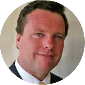
Harvey Kauget practices in the firm's Corporate Practice Group with a focus on intellectual property litigation and prosecution.
Harvey serves a wide-range of clients in the areas of patent, trademark and trade secret litigation, patent and trademark prosecution, IP risk management, portfolio licensing, and client counseling.
Harvey’s litigation and patent prosecution background consists of dealing with matters related to technologies such as: semiconductor processing, plasma dicing, welding systems, lighting and LEDs, hot plates, software, computer integration and networking, satellites, solar power, hydrogen fuel cells, biodiesel, gaming, jewelry, gift cards, cups, davit lift, suntan lotions, power tools, paint rollers, flow systems, nuclear control rods, shirt pressers, air filters, hot water systems, fans, contact lenses, blood plasma expander, disposable blood measuring device, urine analysis, teeth whitening, suture anchors, and medical devices. In addition, he also has experience in a wide-range of other areas including firearms, speakers, waste fuel flare stacks, furniture, exercise equipment, recycling equipment, cement materials, fence posts, and tidal gates.
Mr. Kauget has experience presenting cases before the Court of Appeals for the Federal Circuit and Eleventh Circuit. He is also a registered patent attorney admitted to practice before the U.S. Patent and Trademark office. Before Harvey began his legal career, he worked as an engineer and as a product manager in the semiconductor industry as well as a certified high school chemistry and physics teacher.
Honors & Recognitions
- Listed in The Best Lawyers in America®️, "Lawyer of the Year," Trademark Law, Tampa, Florida (2022 & 2023)
- Listed in The Best Lawyers in America®️, Information Technology Law since 2008, Litigation - Intellectual Property since 2011, Litigation - Patent since 2011, Patent Law since 2011, Technology Law since 2010, Trademark Law since 2011, Trade Secrets Law since 2021
- Named, Chambers USA, Intellectual Property (2021-2022)
- Listed in The Best Lawyers in America®️, "Lawyer of the Year," Patent Law, Tampa, Florida (2015, 2018, 2019, & 2021)
- Florida Trend, "Legal Elite," Intellectual Property Rights (2005, 2007-2008, 2010-2016, 2018, 2020-2021)
- Florida Super Lawyers, Intellectual Property (2009, 2011-2021)
United States
CAST EMG ESD Alliance FlexTech MSIG SOIReceive practical information on designing, writing and protecting your patents from an experienced and knowledgeable source. This course will review the latest thinking in what is a patentable invention and how to protect your invention. You will learn the basics of disclosing your invention for maximizing your protection, with an opportunity for Q&A at the end. A course useful to inventors at every stage of your careers and every stop in our industry ecosystem.