

GRENOBLE, France – June 7, 2022 – With MEMS and imaging sensor innovations driving an explosion in medical, mobility, communications and other Smart applications, the stage is set for the return of SEMI MEMS & Imaging Sensors Summit, 6-7 September, 2022, to the World Trade Center (WTC) in Grenoble, France. More than 400 industry experts will gather for insights into the latest technology developments and trends across the MEMS and sensors supply chain. Registration is open.
 Hosted by SEMI Europe and the MEMS & Sensors Industry Group, a SEMI Technology Community, and Themed Intelligent Sensing for Better and Smarter Living, the summit will open with insightful executive keynotes and feature sessions on the following critical semiconductor industry topics.
Session 1: A Diverse and Sustainable Workforce Enabling Next Generation Innovation
Industry leaders will explore how diversity drives innovation and ways companies and corporate leaders can create an inclusive environment where employees and innovation thrive.
Session 2: Market Brief
Industry trends, market drivers and supply chain dynamics will come into focus.
Session 3: Insights into Emerging Applications
Experts will share their vision for emerging sensor applications and discuss the latest developments in biosensors, MEMS, photonics and spectroscopic technologies.
Session 4: Intelligent Sensing
Discussions will highlight new sensor technologies that enable fast and reliable edge computing to pave the way for smarter applications in industries such as automotive and medical.
Session 5: Technology Showcase
This session will spotlight the latest MEMS and imaging sensor products and applications. Deep and traditional tech companies and startups as well as researchers developing new products will demonstrate cutting-edge solutions. Companies can submit their product demonstration abstracts by June 30.
Session 6.1: MEMS Advancements
Industry leaders will discuss new MEMS technology applications, devices and manufacturing trends. Application topics will include the integration of several sensors into System in Package (SiP), MEMS for medical sensing, and integrating data generation and data processing into the same system. Manufacturing topics will include advancements enabling 300mm wafer sizes, 3D integration and substrate diversification.
Session 6.2: Imaging Advancements
Industry leaders will share their visions for sensing processes, design and computing.
Session 7.1: Environmental MEMS Technology Focus
Future MEMS-enabled environmental technologies that drive advances in everything from preventative maintenance and quality control to environmental monitoring will come into sharp focus.
Session 7.2: The Latest on Short-wave Infrared (SWIR)
This session will explore the latest advancements in traditional SWIR imaging technology from Lynred and the promise of new quantum dot SWIR image sensors from STMicroelectronics and Emberion. It will also cover insights from imec on new consumer applications enabled by affordable sensors, and a low-cost solution for SWIR hyperspectral imaging introduced from VTT.
Session 8: Materials and Equipment Advancements
Experts will discuss how materials and equipment advances are enabling higher performance MEMS devices for new manufacturing techniques and equipment.
Session 9: Optics, Co-Packaged Optics (CPO) and Optical Chips Packaging for MEMS and Imaging Sensors
Rapid growth of cloud data presents new speed and bandwidth requirements. Industry leaders will explore the integration of optics and silicon through CPO to meet growing performance demands and reduce power consumption.
More MEMS & Imaging Sensors Summit Highlights
- Networking opportunities at the exhibition and a gala dinner for attendees of both MEMS and imaging sensor tracks to meet in-person.
- Exhibition showcasing leading companies driving the future of MEMS/imaging and sensors design and manufacturing including:
- ASE Group
- DELO Industrial Adhesives
- Eurofins MASER B.V.
- EV Group (EVG)
- Evatec
- Fraunhofer IPMS
- KLA
- Okmetic Oy
- SAES Getters SpA
- SCHOTT
- SET
- Siemens EDA (represented by EDA Solutions Limited)
Premier sponsors
- Platinum Sponsors: ASE Group, Infineon, KLA, SCHOTT
- Gold Sponsors: Evatec, SUSS MicroTec Group
- Silver Sponsor: AEM
- Event sponsors: Caeleste, EV Group (EVG), JSR Micro N.V., Okmetic
For more information, please visit the MEMS & Sensors Imaging Summit website.
Stay in touch on Twitter @SEMIEurope: #SensorsSummit #MEMS #Imaging #SEMIEurope
About SEMI
SEMI® connects more than 2,500 member companies and 1.3 million professionals worldwide to advance the technology and business of electronics design and manufacturing. SEMI members are responsible for the innovations in materials, design, equipment, software, devices, and services that enable smarter, faster, more powerful, and more affordable electronic products. Electronic System Design Alliance (ESD Alliance), FlexTech, the Fab Owners Alliance (FOA), the MEMS & Sensors Industry Group (MSIG) and SOI Consortium are SEMI Strategic Technology Communities. Visit www.semi.org to learn more, contact one of our worldwide offices, and connect with SEMI on LinkedIn and Twitter.
Association Contact
Serena Brischetto
SEMI Europe
Phone: +49 30 3030 8077-11
Email: [email protected]
 Today, when a GPS signal is lost, commercial PNT solutions use inertial measurement units (IMUs) to maintain positioning accuracy. Over time, however, the accuracy becomes less reliable due to accumulated IMU errors. The initiative aims to drive PNT innovations that pinpoint the position of mobile and stationary assets and enable reliable navigation in critical situations.
  Themed Forward as One – Building A Resilient and Sustainable Electronics Supply Chain in Southeast
 "The global semiconductor equipment industry remains on track to cross the $100 billion threshold for the first time as shown in our latest update of the World Fab Forecast,”said Ajit Manocha, president and CEO of SEMI. “This historic milestone puts an exclamation point on the current run of unprecedented industry growth.”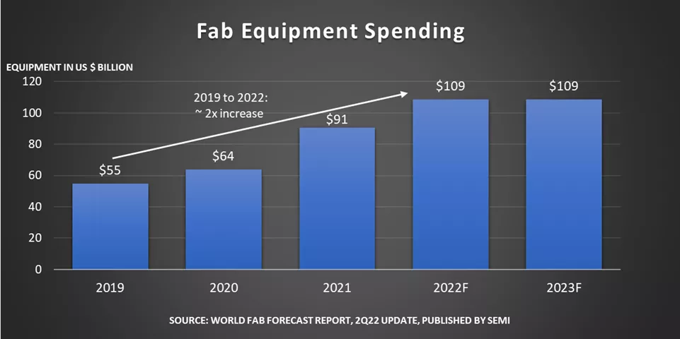

 Themed Resilient Europe: Semiconductors Enabling a Sustainable Digital Life, ISS Europe 2022 will present economic, technology, market, business, and geopolitical developments influencing the global electronics manufacturing industry as well as their implications for strategic business decisions.








 “We applaud Luc Van den hove and Paul Boudre for their excellent work and outstanding research and development leadership and contributions to the European semiconductor community,” said Laith Altimime, president of SEMI Europe.
 Van den hove received his Ph.D. in electrical engineering from the KU Leuven in Belgium. He joined imec in 1984, starting his research career in the field of silicide and interconnect technologies and became manager of the imec micro-patterning group (lithography and dry etching) in 1988. In 1996, Van den hove was appointed department director of unit process step R&D, and in 1998 vice president of the silicon process and device technology division. In January 2007, he was appointed imec EVP and COO and has served as president and CEO of imec since 2009.
 Boudre holds a graduate degree in chemistry from France’s Ecole Nationale Supérieure de Chimie de Toulouse. He joined Soitec in 2007 as Director of Sales, Marketing and Business Development. He has been the CEO since 2015 and a member of the Board of Directors. During his 10 years at KLA-Tencor, he led the group’s European operations, then served as VP for Europe and the U.S. He held management duties in the industrial units of IBM Semiconductor (now part of GlobalFoundries), STMicroelectronics, Motorola Semiconductor (now part of NXP Semiconductors), and Atmel. Boudre has been active in the semiconductor industry for 30 years.
 “Year-over-year first quarter equipment revenue growth is in sync with positive forecasts for 2022 as the semiconductor industry continues its robust increase of fab capacity,” said Ajit Manocha, SEMI president and CEO. “North America and Europe logged healthy quarter-over-quarter rises in equipment spending as they intensify efforts to bolster domestic chipmaking.”
 “Speedy adoption of the European Chips Act will significantly accelerate Europe’s work to attract investments to build up chip manufacturing capacity and R&D,” said Laith Altimime, president of SEMI Europe. “The Act is also a key step forward for Europe to substantially decarbonize semiconductor manufacturing and drive digital transformation.”
 “As global demand for semiconductors continues to grow, Michigan is poised to be a solution provider for semiconductor shortages and puts companies in the heart of semiconductor and battery R&D efforts nationwide,” said Governor Gretchen Whitmer. “Michigan is one of only three states that will be launching planning work to define curricula to support employers in the semiconductor industry. With this new apprenticeship program, along with our global manufacturing and automotive R&D leadership, we are leading the charge in addressing the universal industry demand for semiconductors while creating good jobs for Michigan workers.”