downloadGroupGroupnoun_press release_995423_000000 copyGroupnoun_Feed_96767_000000Group 19noun_pictures_1817522_000000Member company iconResource item iconStore item iconGroup 19Group 19noun_Photo_2085192_000000 Copynoun_presentation_2096081_000000Group 19Group Copy 7noun_webinar_692730_000000Path
Skip to main content
Default Banner Image

United States

MILPITAS, Calif. – April 12, 2022 – Worldwide sales of semiconductor manufacturing equipment in 2021 surged 44% to an all-time record of $102.6 billion from $71.2 billion in 2020, SEMI, the industry association representing the global electronics product design and manufacturing supply chain, reported today. The data is now available in the Worldwide Semiconductor Equipment Market Statistics (WWSEMS) Report.

SEMI logoChina claimed the largest market for semiconductor equipment for the second time with sales expanding 58% to $29.6 billion to mark the fourth consecutive year of growth. Korea, the second-largest equipment market, registered a sales increase of 55% to $25.0 billion, after showing strong growth in 2020. Taiwan logged 45% growth to $24.9 billion to claim the third position. Annual semiconductor equipment spending increased 23% in Europe and 17% in North America, which continues to recover from a contraction in 2020. Sales in Rest of the World jumped 79% in 2021.

“The 44% increase in manufacturing equipment spending in 2021 highlights the global semiconductor industry’s aggressive push to add capacity,” said Ajit Manocha, SEMI president and CEO. “This drive to expand production capabilities extends beyond the current supply imbalance, as the industry continues to ramp up to address a wide range of emerging high-tech applications that will enable a smarter digital world with countless social benefits.”

Global sales of wafer processing equipment rose 44% in 2021, while other front-end segment sales grew 22%. Assembly and packaging showed exceptional growth across all regions, resulting in an 87% market increase in 2021, while total test equipment sales rose 30%.

Compiled from data submitted by members of SEMI and the Semiconductor Equipment Association of Japan (SEAJ), the Worldwide SEMS Report is a summary of the monthly billings figures for the global semiconductor equipment industry. Equipment categories cover wafer processing, assembly and packaging, test, and other front-end equipment including mask/reticle manufacturing, wafer manufacturing, and fab facilities.

Annual Billings by Region in Billions of U.S. Dollars with Year-Over-Year Change Rates

Region

2021

2020

% Change

China

29.62

18.72

58%

Korea

24.98

16.08

55%

Taiwan

24.94

17.15

45%

Japan

7.80

7.58

3%

North America

7.61

6.53

17%

Rest of the World

4.44

2.48

79%

Europe

3.25

2.64

23%

Total

102.64

71.19

44%

Source: SEMI (www.semi.org) and SEAJ (www.seaj.or.jp), April 2022


The SEMI Equipment Market Data Subscription (EMDS) provides comprehensive market data for the global semiconductor equipment market. The subscription includes three reports:

  • Monthly SEMI Billings Report, a perspective on equipment market trends
  • Monthly Worldwide Semiconductor Equipment Market Statistics (WWSEMS), a detailed report of semiconductor equipment billings for seven regions and 24 market segments
  • SEMI Semiconductor Equipment Forecast, an outlook for the semiconductor equipment market

For more information or to subscribe, please contact the SEMI Industry Research and Statistics Group at [email protected]. More information is also available online.


About SEMI
SEMI® connects more than 2,500 member companies and 1.3 million professionals worldwide to advance the technology and business of electronics design and manufacturing. SEMI members are responsible for the innovations in materials, design, equipment, software, devices, and services that enable smarter, faster, more powerful, and more affordable electronic products. Electronic System Design Alliance (ESD Alliance), FlexTech, the Fab Owners Alliance (FOA), the MEMS & Sensors Industry Group (MSIG) and SOI Consortium are SEMI Strategic Technology Communities. Visit www.semi.org to learn more, contact one of our worldwide offices, and connect with SEMI on LinkedIn and Twitter.

Association Contact
Michael Hall/SEMI
Phone: 1.408.943.7988
Email: [email protected]

MILPITAS, Calif. — April 11, 2022 — Semiconductor manufacturers worldwide are on track to boost 200mm fab capacity by 1.2 million wafers, or 21%, from the start of 2020 to the end of 2024 to hit a record high of 6.9 million wafers per month, SEMI announced today in its 200mm Fab Outlook Report. After climbing to $5.3 billion last year, 200mm fab equipment spending is expected to be $4.9 billion in 2022 as 200mm fab utilization remains at high levels and the global semiconductor industry works to overcome the chip shortage.

SEMI logo“Wafer manufacturers will add 25 new 200mm lines over the five-year period to help meet growing demand for applications such as 5G, automotive and Internet of Things (IoT) devices that rely on devices like analog, power management and display driver integrated circuits (ICs), MOSFETs, microcontroller units (MCUs) and sensors,” said Ajit Manocha, SEMI president and CEO.

The SEMI 200mm Fab Outlook Report, covering the 12 years from 2013 to 2024, also reveals that foundries will account for more than 50% of fab capacity worldwide this year, followed by analog at 19% and discrete/power at 12%. Regionally, China will lead the world in 200mm capacity with 21% share in 2022, followed by Japan with 16% and Taiwan and Europe/Mideast at 15% each.
 

200mm Fab Report chart

200mm installed semiconductor capacity and fab count, 2013 to 2024*


* Fab count is net of wafer-size conversions.


Equipment investments are projected to remain above $3 billion in 2023, with the foundry sector accounting for 54%, followed by discrete/power at 20% and analog at 19%.

The SEMI 200mm Fab Outlook Report lists more than 330 fabs and lines and includes 64 changes across 47 fabs since its most recent update in September 2021.

About SEMI

SEMI® connects more than 2,500 member companies and 1.3 million professionals worldwide to advance the technology and business of electronics design and manufacturing. SEMI members are responsible for the innovations in materials, design, equipment, software, devices, and services that enable smarter, faster, more powerful, and more affordable electronic products. Electronic System Design Alliance (ESD Alliance), FlexTech, the Fab Owners Alliance (FOA), the MEMS & Sensors Industry Group (MSIG) and SOI Consortium are SEMI Strategic Technology Communities. Visit www.semi.org to learn more, contact one of our worldwide offices, and connect with SEMI on LinkedIn and Twitter.

Association Contacts

Michael Hall/SEMI
Phone: 1.408.943.7988
Email: [email protected]

Christian G. Dieseldorff/SEMI
Phone: 1.408.943.7940
Email: [email protected]

HALF MOON BAY, Calif. — April 5, 2022 — SEMI Industry Strategy Symposium (ISS) 2022 opened yesterday with the theme Semiconductors Leading a Transforming World to highlight semiconductor industry growth opportunities and challenges. The annual three-day conference of C-level and senior industry executives gives a comprehensive outlook of global electronics manufacturing, examining international economic, technology, market, business and geopolitical developments influencing the industry. 

ISS logo
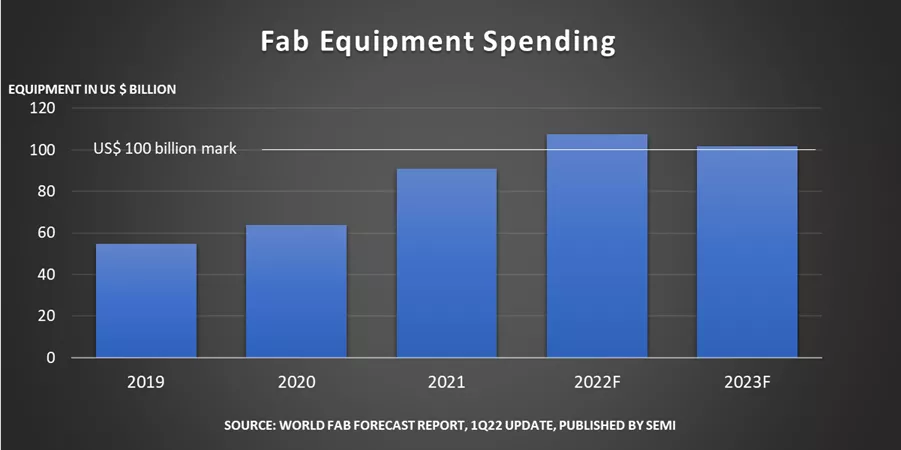
Today, the second day of the April 4-6 conference, will feature deep discussions on key issues including the next decade of semiconductor innovation, deep learning hardware, artificial intelligence (AI) in healthcare, automotive and mobility, sustainability, trends in deposition technologies and advanced packaging, and the role of chip design in new product innovation. Day three will be marked by discussions on quantum computing and the resurgence of 200mm manufacturing and also convene a panel on the $100 billion wafer fab equipment frontier.

Yesterday, opening keynote speaker Mark Papermaster, CTO and Executive Vice President of Technology and Engineering at AMD, observed that “the vast amount of data today is automatically generated. We are in a day of complete data overload.” Together, machine learning and AI are key in putting “data efficiently to work.” The accuracy of machine learning in analyzing “reams of data and recognizing patterns is simply astounding and has revolutionized the chip industry” by enabling AI to mimic decision-making, he said. AI will also “tremendously speed chip design.”

Higher compute performance is driving semiconductor innovation, and vertically stacking chip components has emerged as one way the industry is meeting the demand. “The need for more high-performance computing is phenomenal,” Papermaster said. “Once you start thinking in 3D, everything is different. It is an innovation engine,” he noted. Optical interconnects that enable bandwidth improvements will also drive performance gains. Papermaster called on the chip industry to “continue to work together on heterogeneous architectures, emphasizing that “new computing architectures require deep collaboration among semiconductor ecosystems.”                                                 

In the Economic Trends session, presenters took on macroeconomic trends and detailed industry-specific forecasts:  

Tim Mahedy, Senior Economist at KPMG Economics, noted that Organisation for Economic Co-operation and Development (OECD) economies saw strong growth rates in March and that many developing economies are back to pre-pandemic levels. While the war in Ukraine caused commodity prices to surge, Mahedy noted the conflict poses little risk to the U.S. economy since the linkages across U.S. and Russia trade and banking are “not strong.” He said “the global economy is slowly starting to heal” from the shocks of the pandemic and that, in the U.S., “consumers will drive the economy in 2022.” Mahedy sees the probability of recession low, at about 10%. “We don’t appear to be entering a period of economic contraction.” Mahedy added. “There’s a lot of reason for optimism that once we get through current geopolitical events we’ll still be on very strong footing.”

Michael Yang, Senior Director of Semiconductors Research at OMDIA, a spinoff of IHS Markit, said that every segment of the industry grew in 2021 as it reached record revenue of $587 billion, and “nine companies of the top 10 logged double-digital revenue growth.” From 2019 through 2021, the semiconductor industry saw a “historic 36% revenue increase.” Top semiconductor growth drivers over the next five years will include the buildout of the metaverse as it increases smartphone demand; continuing cloud infrastructure expansion driven by AI, machine learning and other leading-edge technologies; and automotive as the industry sees hockey-stick growth of electric vehicles. While the pandemic drove surging demand for consumer and business PCs in 2020, Yang expects demand “to drop back to pre-pandemic levels or lower” this year.

Inna Skvortsova, Market Analyst on the Market Intelligence Team at SEMI, observed that global GDP is set to grow at 4.4% GDP this year and expand again in 2023. This year, electronic end-use markets are expected to remain robust on the strength of emerging applications. For its part, “the semiconductor industry is performing extremely well,” she noted, with projected revenue growth of 9.4% in 2022. The total materials market is forecast to grow 6.7% in 2022, with wafer fab materials expanding 8.4% and packaging materials rising 3.9%. Potential industry headwinds include inflationary pressures, ongoing trade and export restrictions and geopolitical conflicts, and the industry talent shortage.

Jan Vardaman, President and Founder of TechSearch International, said the adoption of advanced packaging is fueled by key performance metrics such as low latency, bandwidth and data rates, better power efficiency, IO density and routing density increases. “We’re in a new era of semiconductor packaging,” Vardaman said. “Chiplets will be a key enabler over the next 10 to 20 years. You have to think of your design in a different way, changing from silicon-centric thinking to system-level planning and co-design of IC and packages.” She said that a new era of heterogeneous integration (HI) including chiplets has spawned with a variety of solutions that require a robust HI ecosystem. The solutions include organic substrate, embedded bridge on laminate, fan-out on substrate with embedded bridge, and 3D stack.

Andrea Lati, Vice President of Market Research at TechInsights, noted “the outlook is looking very bright for the IC industry” as structural changes and secular drivers such as the data economy and AI accelerate the growth of the semiconductor and chip equipment markets. While IC inventories are tight and expected to remain elevated through the rest of the year, they are rising. Shipments of 5G ICs for smartphones are forecast to grow 20% in 2022 while automotive is expected to see an 18% increase in IC shipments this year. Over the longer term, Lati sees IC shipment growth accelerating from mid-single digits over the past decade to high single digits over the next decade. New IC investments include more than $120 billion over the next two years primarily in logic and foundry. Capital expenditures for advanced logic and foundry are expected to increase 30% driven by Intel, GlobalFoundries and TSMC.

Bob Johnson, Vice President at Gartner, forecasts that semiconductor industry revenue will reach $790 billion in 2026, growing at a just below 6% CAGR to reach $1 trillion in revenue in the next 10 to 12 years. Growth drivers include AI, electric vehicles, advanced driver-assisted systems, cloud and edge computing, 5G and the metaverse. Reaching that milestone will require not only a volume increase but a higher average selling price (ASP). He also cautioned that “the industry will need to find the resources to double its size from 2020” such as an expanded workforce, more real estate for new facilities, and the funding to finance it all. “The bottom line is that it’s going to take a lot of money.”

The Economic Trends session concluded with a panel on the semiconductor industry outlook moderated by Clark Fuhs, senior director of Corporate Analytics at Lam Research with Yang, Vardaman, Lati, Johnson and Mario Morales, group vice president of Enabling Technologies and Semiconductors at IDC.

The afternoon session focused on Market Perspectives on geopolitics and post-COVID supply chains:

Chase Blazek, Asia Pacific Analyst at RANE, addressing U.S.-China trade relations, said that “now we’re competing more than we’re cooperating,” adding that “U.S. politics is united on hawkishness on China.” He sees a 75% likelihood of tensions between China and Taiwan increasing over the next five years with no war. Despite the cross-strait tensions and the ongoing trade war between the U.S and China, he expects U.S-Sino and China-Taiwan relations and industrial supply chains to remain stable. One reason is the interdependence of China and Taiwan in semiconductor trade: China needs chips made in Taiwan to grow its semiconductor industry, and China is a key Taiwan chip customer. 

Bindiya Vakil, CEO and Founder of Resilinc, noting that modern supply chains face over 200 disruptive events weekly on a global level, said that semiconductor companies need greater visibility into their supply chains to increase resilience and reduce risk. “We really don’t understand the supply chain networks we live in,” she said. “The world is changing at a pace faster than supply chains can keep up with.” Company procurement departments must shift from reacting to supply chain changes to anticipating disruptions by outlining worst-case scenarios, deepening collaborations with supply chain partners, and taking deliberate action. “Understanding the supply chain is critical,” she said. An important step companies can take is to work with supply chain partners by focusing first on continuity and risk management, not on cost.

Day one ended with comments on the U.S. CHIPS Act objectives and implementation from Sreenivas Ramaswamy, senior policy advisor in the Office of Policy and Strategic Planning at the United States Department of Commerce, followed by a panel on U.S. semiconductor incentives moderated by Joe Pasetti, vice president of global public policy and advocacy at SEMI, with Ian Steff, president and CEO of mySilicon Compass and Gene Irisari, vice president and head of semiconductor policy at Samsung Electronics America.

Day two and three presenters will include Google, Intel, Micron Technology, NVIDIA, Varian Medical Systems, Center of Automotive Research, Lam Research, National Gem Consortium, Tosoh Quartz, imec, ASM International, IC Knowledge, Synopsys and SEMI.

The SEMI Industry Strategy Symposium (ISS) examines global economic, technology, market, business and geopolitical developments influencing the global electronics manufacturing industry along with their implications for strategic business decisions. For more than 35 years, ISS has been the premier semiconductor conference for senior executives to acquire the latest trend data, technology highlights and industry perspective to support business decisions, customer strategies and the pursuit of greater profitability.
 

About SEMI

SEMI® connects more than 2,500 member companies and 1.3 million professionals worldwide to advance the technology and business of electronics design and manufacturing. SEMI members are responsible for the innovations in materials, design, equipment, software, devices, and services that enable smarter, faster, more powerful, and more affordable electronic products. Electronic System Design Alliance (ESD Alliance), FlexTech, the Fab Owners Alliance (FOA), the MEMS & Sensors Industry Group (MSIG) and SOI Consortium are SEMI Strategic Technology Communities. Visit www.semi.org to learn more, contact one of our worldwide offices, and connect with SEMI on LinkedIn and Twitter.
 

Association Contact 

Michael Hall/SEMI 
Email: [email protected] 
Phone: 1.408.943.7988

MILPITAS, Calif. April 4, 2022 — Electronic System Design (ESD) industry revenue increased 14.4% from $3,031.5 million in Q4 2020 to $3,468.2 million in Q4 2021, the ESD Alliance, a SEMI Technology Community, announced today in its latest Electronic Design Market Data (EDMD) report. The four-quarter moving average, which compares the most recent four quarters to the prior four, rose 15.8%.   

SEMI ESDA lockup logo“The industry continued to report double-digit year-over-year revenue growth for Q4 2021 and ended 2021 with $13.2 billion total market revenue,” said Walden C. Rhines, Executive Sponsor of the SEMI Electronic Design Market Data report. “Product categories Computer-Aided Engineering, Printed Circuit Board and Multi-Chip Module,  Semiconductor Intellectual Property, and Services recorded double-digit growth for the quarter. Geographically, the Americas; Europe, Middle East, and Africa (EMEA); and Asia Pacific (APAC) all reported revenue growth.”

The companies tracked in the EDMD report employed 51,236 people globally in Q4 2021, a 5.7% increase over the Q4 2020 headcount of 48,478 and up 0.1% compared to Q3 2021.

The quarterly EDMD report contains detailed revenue information with the following category and geographic breakdowns.

Revenue by Product and Application Category – Year-Over-Year Change

  • Computer-Aided Engineering (CAE) revenue increased 11.2% to $1,064.6 million. The four-quarter CAE moving average increased 12.2%.
  • IC Physical Design and Verification revenue decreased 2% to $624.5 million. The four-quarter moving average for the category rose 7%.
  • Printed Circuit Board and Multi-Chip Module (PCB and MCM) revenue increased 13.9% to $333.7 million. The four-quarter moving average for PCB and MCM rose 15.1%.
  • Semiconductor Intellectual Property (SIP) revenue jumped 24.8% to $1,314.3 million. The four-quarter SIP moving average grew 23.9%.
  • Services revenue increased 43.1% to $131.1 million. The four-quarter Services moving average increased 19%.

Revenue by Region – Year-Over-Year Change

  • The Americas, the largest reporting region by revenue, procured $1,577.2 million of electronic system design products and services in Q4 2021, a 21% increase. The four-quarter moving average for the Americas rose 17.2%.
  • Europe, Middle East, and Africa (EMEA) procured $482.5 million of electronic system design products and services in Q4 2021, a 5.5% increase. The four-quarter moving average for EMEA grew 12.6%.
  • Japan’s procurement of electronic system design products and services decreased 2.4% to $222.8 million. The four-quarter moving average for Japan rose 1%.
  • Asia Pacific (APAC) procured $1,185.6 million of electronic system design products and services in Q4 2021, a 13.8% increase. The four-quarter moving average for APAC increased 18.9%.

About the EDMD Report

The ESD Alliance Electronic Design Market Data (formerly the Market Statistics Service) report presents Electronic Design Automation (EDA), SIP and services industry revenue data quarterly. Both public and private companies contribute data to the report available from SEMI. Each quarterly report is published approximately three months after quarter close. EDMD report data is segmented as follows:

  • Revenue by product category (CAE, IC Physical Design and Verification, Semiconductor IP, PCB/MCM Layout, and Services) including numerous detailed sub-categories
  • Revenue by geographic region (Americas, EMEA, Japan and APAC)
  • Total employment at participating companies

For information about SEMI market research reports, visit the SEMI Market Research Reports and Databases Catalog.

About the Electronic System Design Alliance

The Electronic System Design (ESD) Alliance, a SEMI Technology Community, is the central voice to communicate and promote the value of the semiconductor design ecosystem as a vital component of the global electronics industry. As an international association of companies providing goods and services throughout the semiconductor design ecosystem, it is a forum to address technical, marketing, economic and legislative issues affecting the entire industry. For more information about the ESD Alliance, visit http://esd-alliance.org.

About SEMI

SEMI® connects more than 2,500 member companies and 1.3 million professionals worldwide to advance the technology and business of electronics design and manufacturing. SEMI members are responsible for the innovations in materials, design, equipment, software, devices, and services that enable smarter, faster, more powerful, and more affordable electronic products. Electronic System Design Alliance (ESD Alliance), FlexTech, the Fab Owners Alliance (FOA), the MEMS & Sensors Industry Group (MSIG) and SOI Consortium are SEMI Strategic Technology Communities. Visit www.semi.org to learn more, contact one of our worldwide offices, and connect with SEMI on LinkedIn and Twitter.

The information supplied by the ESD Alliance is believed to be accurate and reliable, but the ESD Alliance assumes no responsibility for any errors that may appear in this document. All trademarks and registered trademarks are the property of their respective owners.

Press Contacts                                                                                 

Paul Cohen
ESD Alliance
SEMI Technology Community
978-769-2106             

Jack Taylor
Siemens EDA PR
Siemens Digital Industries Software
512-560-7143 

Posthumous Recognition for Individuals who made Significant, Noteworthy Contributions to Industry

MILPITAS, Calif. April 4, 2022 Nominations opened today for the Phil Kaufman Hall of Fame for Distinguished Contributions to Electronic System Design sponsored by the Electronic System Design Alliance (ESD Alliance) and the IEEE Council on Electronic Design Automation (CEDA).

The honor posthumously recognizes individuals who made significant and noteworthy contributions through creativity, entrepreneurism and innovation to the electronic system design industry and were not recipients of the Phil Kaufman Award. Deceased members of the community are not eligible to receive the Phil Kaufman Award, a policy set by the IEEE.

SEMI ESDA CEDA logo

Selections for the Hall of Fame are determined through a nomination process. Nominations are reviewed by the ESD Alliance and IEEE CEDA Kaufman Award selection committees. A special Phil Kaufman Hall of Fame page on the ESD Alliance and IEEE CEDA websites will host photos, citations and tributes to the selected inductees.

The nomination period runs through Friday, April 29, and inductees will be announced in June. The link to the nomination form can be found here. Nominations submitted in 2021 will be valid through 2023.

Inaugural honorees awarded in 2021 were Jim Hogan, executive, angel investor and board member, and Stanford University Professor Edward J. McCluskey, acknowledged for their significant and noteworthy contributions to the electronic system design industry.

About the Electronic System Design Alliance

The Electronic System Design (ESD) Alliance, a SEMI Technology Community representing members in the electronic system and semiconductor design ecosystem, is a community that addresses technical, marketing, economic and legislative issues affecting the entire industry. It acts as the central voice to communicate and promote the value of the semiconductor design ecosystem as a vital component of the global electronics industry. Visit www.semi.org/en/communities/esda to learn more.

Follow the ESD Alliance

ESD Alliance Bridging the Frontier blog
Twitter: @ESDAlliance
LinkedIn
Facebook

About SEMI

SEMI® connects more than 2,500 member companies and 1.3 million professionals worldwide to advance the technology and business of electronics design and manufacturing. SEMI members are responsible for the innovations in materials, design, equipment, software, devices, and services that enable smarter, faster, more powerful, and more affordable electronic products. Electronic System Design Alliance (ESD Alliance), FlexTech, the Fab Owners Alliance (FOA), the MEMS & Sensors Industry Group (MSIG) and SOI Consortium are SEMI Strategic Technology Communities. Visit www.semi.org to learn more, contact one of our worldwide offices, and connect with SEMI on LinkedIn and Twitter.

About the IEEE Council on Electronic Design Automation (CEDA)

The IEEE Council on Electronic Design Automation (CEDA) provides a focal point for EDA activities spread across seven IEEE societies (Antennas and Propagation, Circuits and Systems, Computer, Electron Devices, Electronics Packaging, Microwave Theory and Techniques, and Solid-State Circuits). The Council sponsors or co-sponsors over a dozen key EDA conferences including: the Design Automation Conference (DAC), Asia and South Pacific Design Automation Conference (ASP-DAC), International Conference on Computer-Aided Design (ICCAD), Design Automation and Test in Europe (DATE), and events at Embedded Systems Week (ESWEEK). The Council also publishes IEEE Transactions on Computer-Aided Design of Integrated Circuits & Systems (TCAD), IEEE Design & Test (D&T), and IEEE Embedded Systems Letters (ESL). The Council boasts a prestigious awards program in order to promote the recognition of leading EDA professionals, which includes the A. Richard Newton, Phil Kaufman, and Ernest S. Kuh Early Career Awards. The Council welcomes new volunteers and local chapters.

Stay in touch with IEEE CEDA:

Website: www.ieee-ceda.org
LinkedIn: https://www.linkedin.com/groups/8343531
Facebook: https://www.facebook.com/ieeeceda/
Twitter: https://twitter.com/IEEECEDA

All trademarks and registered trademarks are the property of their respective owners.

Association Contacts

Nanette Collins
Public Relations for the ESD Alliance                         
Email: [email protected]  

Michael Hall/SEMI
Email: [email protected]

Amanda Osborn
IEEE Council on EDA
[email protected]

Award Ceremony and Banquet Hosted by the ESD Alliance and IEEE CEDA

MILPITAS, CALIF. March 28, 2022 Dr. Anirudh Devgan, President and CEO of Cadence Design Systems, will be honored with the 2021 Phil Kaufman Award for Distinguished Contributions to Electronic System Design at an award ceremony and banquet Thursday, May 12.

Hosted by the Electronic System Design Alliance (ESD Alliance) and the IEEE Council on Electronic Design Automation (CEDA), the celebration will be held from 6:30 p.m. until 9:30 p.m. at The GlassHouse, 2 South Market Street in San Jose, Calif.

SEMI ESDA CEDA logo

Early bird pricing for tickets is available through Friday, April 8, at $175 per individual from member companies and $225 each for non-members. Member tickets after April 8 are $225 each and $275 per non-member. Member pricing is offered for individuals in companies that are active SEMI members or active IEEE members.

Sponsorship opportunities are available. Contact Bob Smith, executive director of the ESD Alliance, at [email protected] for more information.

Registration, COVID-19 protocols and additional details can be found on the 2021 Phil Kaufman Award ceremony and banquet page.

About the Phil Kaufman Award

The Phil Kaufman Award honors individuals who have had a demonstrable impact on the field of electronic system design through technology innovations, education/mentoring, or business or industry leadership. The award was established as a tribute to Phil Kaufman, the late industry pioneer who turned innovative technologies into commercial businesses that have benefited electronic designers. The 2019 recipient was Dr. Mary Jane Irwin, Evan Pugh Professor and A. Robert Noll Chair Emeritus in Engineering in the Department of Computer Science and Engineering at Pennsylvania State University.

Due to the COVID-19 pandemic, no award was given for 2020.

Nominations are open for the 2022 Phil Kaufman Award. The deadline to submit nomination forms for the 2022 Phil Kaufman Award is Thursday, June 30.
 

About the Electronic System Design Alliance

The Electronic System Design (ESD) Alliance, a SEMI Technology Community representing members in the electronic system and semiconductor design ecosystem, is a community that addresses technical, marketing, economic and legislative issues affecting the entire industry. It acts as the central voice to communicate and promote the value of the semiconductor design ecosystem as a vital component of the global electronics industry. Visit www.semi.org/en/communities/esda to learn more.

Follow the ESD Alliance

ESD Alliance Bridging the Frontier blog
Twitter: @ESDAlliance
LinkedIn
Facebook

About SEMI

SEMI® connects more than 2,500 member companies and 1.3 million professionals worldwide to advance the technology and business of electronics design and manufacturing. SEMI members are responsible for the innovations in materials, design, equipment, software, devices, and services that enable smarter, faster, more powerful, and more affordable electronic products. Electronic System Design Alliance (ESD Alliance), FlexTech, the Fab Owners Alliance (FOA), the MEMS & Sensors Industry Group (MSIG) and SOI Consortium are SEMI Strategic Technology Communities. Visit www.semi.org to learn more, contact one of our worldwide offices, and connect with SEMI on LinkedIn and Twitter.

About the IEEE Council on Electronic Design Automation (CEDA)

The IEEE Council on Electronic Design Automation (CEDA) provides a focal point for EDA activities spread across seven IEEE societies (Antennas and Propagation, Circuits and Systems, Computer, Electron Devices, Electronics Packaging, Microwave Theory and Techniques, and Solid-State Circuits). The Council sponsors or co-sponsors over a dozen key EDA conferences including: the Design Automation Conference (DAC), Asia and South Pacific Design Automation Conference (ASP-DAC), International Conference on Computer-Aided Design (ICCAD), Design Automation and Test in Europe (DATE), and events at Embedded Systems Week (ESWEEK). The Council also publishes IEEE Transactions on Computer-Aided Design of Integrated Circuits & Systems (TCAD), IEEE Design & Test (D&T), and IEEE Embedded Systems Letters (ESL). The Council boasts a prestigious awards program in order to promote the recognition of leading EDA professionals, which includes the A. Richard Newton, Phil Kaufman, and Ernest S. Kuh Early Career Awards. The Council welcomes new volunteers and local chapters.

Stay in touch with IEEE CEDA

Website: www.ieee-ceda.org
LinkedIn: https://www.linkedin.com/groups/8343531
Facebook: https://www.facebook.com/ieeeceda/
Twitter: https://twitter.com/IEEECEDA

All trademarks and registered trademarks are the property of their respective owners.

Association Contacts

Nanette Collins/ESD Alliance                          
Email: [email protected]  

Michael Hall/SEMI
Email: [email protected]

The SEMI Foundation partners with Foothill College, Ignited Education, and Krause Center for Innovation to develop microelectronics career training program.

MILPITAS, Calif. — March 29, 2022 — SEMI, the global industry association representing the electronics manufacturing and design supply chain, today announced that, in partnership with Ignited Education, Foothill College and Krause Center for Innovation, it has won a $1 million California Apprenticeship Initiative (CAI) New and Innovative Grant for the development of a semiconductor pre-apprenticeship and apprenticeship program to expand the pathway to careers in the microelectronics industry. The SEMI Foundation and its partners will develop the industry career training program to be offered by California community colleges and ultimately schools in other states. The program will connect CAI partners with SEMI member companies to define job competencies that shape the coursework.   

SEMI logo
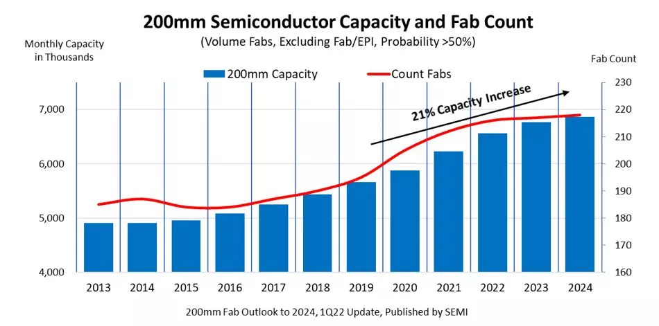
The CAI funding will support the SEMI Foundation’s work to build the SEMI Career and Apprenticeship Network (SCAN), aimed at helping overcome the U.S. microelectronics industry’s talent shortage as the federal government continues to invest in apprenticeships. The grant also supports the foundation’s efforts to promote a more inclusive workforce. SCAN will offer training that equips workers with the technical skills needed to enter high-demand, entry-level jobs in the microelectronics industry. It will also expand the pool of skilled workers for hiring companies.

“Securing the CAI funding is a key step in building out SCAN as we work to develop a national apprenticeship network, recruit more people of color and women to the industry, and create industry credentials recognized nationwide,” said Shari Liss, executive director of the SEMI Foundation. “We look forward to continuing the vital work with our partners to expand access to jobs across the semiconductor industry and enable more people to enter rewarding careers.”

CAI New and Innovative Grants fund the development of pre-apprenticeship and apprenticeship programs to strengthen sectors that drive economic growth while creating opportunities for workers in underserved communities to enter high-wage professions. CAI funds workforce development projects across 20 sectors including advanced manufacturing, global trade and logistics, agriculture, energy and life sciences to help build connections between students and employers.

Foothill College will develop coursework covering the competencies for various high-need positions in the microelectronics industry. Complementing the work of Foothill College to reach students early in their education, Ignited and the Krause Center for Innovation will create middle school foundations and high-school pathways pre-apprenticeship programs featuring engaging student experiences and teacher-training workshops. The SEMI Foundation will ensure the programs meet the industry’s workforce needs.  

“Talent pipelines are powerful,” said Jeff Schmidt, Chief Executive Officer of Santa Clara, Calif.-based Ignited. “They open new doors, offer experiences that shape us, and provide role models that inspire our career choices. SCAN will build a strong, compelling pre-apprenticeship and apprenticeship pipeline that will change the lives of students and families that need it most. We’re proud to support the SEMI Foundation and this amazing group of partners who are doing such critical work for the microelectronics industry.”

"Foothill College is proud to partner with SEMI,” said Chris Allen, Dean of Apprenticeship Programs at Foothill College, based in Los Altos Hills, Calif. “This is an exciting opportunity for our faculty to collaborate with the microelectronics industry to help align work competencies with curriculum development. We look forward to building this new and innovative apprenticeship pathway at this crucial time in the redevelopment of the U.S. semiconductor manufacturing industry.”

SEMI member companies, government agencies and other industry stakeholders interested in developing or participating in microelectronics apprenticeship programs can contact the SEMI Foundation at [email protected].

About the SEMI Foundation

The SEMI Foundation is a 501(c)(3) nonprofit charitable organization founded in 2001 to support economic opportunity for workers and the sustained growth of the microelectronics industry. The Foundation works to attract, develop, and retain a well-trained and innovative workforce through educational programs, diversity initiatives to support women, veterans, and people of color, and member engagement. The Foundation’s longest-running program, SEMI High Tech U, inspires high-school students to pursue STEM college educations and careers. Since 2002, High Tech U programs in Austria, France, Japan, Korea, Netherlands, Singapore, Taiwan and the United States have directly influenced and inspired more than 8,200 students and teachers.

About SEMI

SEMI® connects more than 2,500 member companies and 1.3 million professionals worldwide to advance the technology and business of electronics design and manufacturing. SEMI members are responsible for the innovations in materials, design, equipment, software, devices, and services that enable smarter, faster, more powerful, and more affordable electronic products. Electronic System Design Alliance (ESD Alliance), FlexTech, the Fab Owners Alliance (FOA), the MEMS & Sensors Industry Group (MSIG) and SOI Consortium are SEMI Strategic Technology Communities. Visit www.semi.org to learn more, contact one of our worldwide offices, and connect with SEMI on LinkedIn and Twitter.

Association Contact

Michael Hall/SEMI
Phone: 1.408.943.7988
Email: [email protected]

Industry drive to expand and upgrade capacity to push spending over $100 billion for first time

MILPITAS, Calif. — March 22, 2022 — Global fab equipment spending for front-end facilities is expected to jump 18% year-over-year (YOY) to an all-time high of US$107 billion in 2022, marking a third consecutive year of growth following a 42% surge in 2021, SEMI announced today in its latest quarterly World Fab Forecast report.

SEMI logo“Crossing the $100 billion mark in spending on global fab equipment for the first time is a historic ​milestone for the semiconductor industry,” said Ajit Manocha, president and CEO of SEMI. “This ​significant achievement is a tribute to the relentless drive to add and upgrade capacity to address a diverse range of markets and emerging applications, solidifying expectations for long-term industry growth to enable electronics for the digital world.” 

“Global fab equipment spending is forecast to have another healthy year in 2023 and is expected to remain above the $100 billion mark,” said Sanjay Malhotra, vice president of Corporate Marketing and the Market Intelligence Team at SEMI. “We expect global semiconductor capacity to maintain steady growth this year and in 2023.”
 

World Fab Forecast chart

 
Fab Equipment Spending by Region

Taiwan is expected to lead fab equipment spending in 2022, increasing investments 56% YoY to US$35 billion, followed by Korea at US$26 billion, a 9% rise, and China at US$17.5 billion, a 30% drop from its peak last year. Europe/Mideast is forecast to log record high spending of US$9.6 billion this year, and while comparatively smaller, this would represent a staggering growth of 248% YoY. Taiwan, Korea and Southeast Asia are also expected to register record high investments in 2022. In the Americas, the report shows fab equipment spending peaking at US$9.8 billion by 2023.

Industry Continues to Boost Capacity

The SEMI World Fab Forecast report shows the global industry increasing capacity 8% this year after a 7% rise in 2021. Capacity growth is expected to continue increasing, rising 6% in 2023. The fab equipment industry last saw a YoY installed capacity growth rate of 8% in 2010, when it topped 16 million wafers per month (200mm equivalents) – nearly half of the 29 million wafers per month (200mm equivalents) projected for 2023.

Over 83% of equipment spending in 2022 will stem from capacity increases at 150 fabs and production lines, a proportion expected to edge down to 81% next year as 122 known fabs and lines add capacity.  

As expected, the foundry sector, with a share of about 50%, will account for the bulk of equipment spending in 2022 and 2023, followed by memory at 35%. The two sectors also represent most of the capacity increases.

The SEMI World Fab Forecast report lists 1,426 facilities and lines globally, including 124 future facilities and lines with various probabilities that are expected to start volume production no sooner than 2022.
 

About SEMI

SEMI® connects more than 2,500 member companies and 1.3 million professionals worldwide to advance the technology and business of electronics design and manufacturing. SEMI members are responsible for the innovations in materials, design, equipment, software, devices, and services that enable smarter, faster, more powerful, and more affordable electronic products. Electronic System Design Alliance (ESD Alliance), FlexTech, the Fab Owners Alliance (FOA), the MEMS & Sensors Industry Group (MSIG) and SOI Consortium are SEMI Strategic Technology Communities. Visit www.semi.org to learn more, contact one of our worldwide offices, and connect with SEMI on LinkedIn and Twitter.

Association Contacts

Michael Hall/SEMI
Phone: 1.408.943.7988
Email: [email protected]

Christian G. Dieseldorff/SEMI
Phone: 1.408.943.7940
Email: [email protected]  

Featuring Executives from Industry Leaders Arm, Cadence, D2S, Keysight, Siemens EDA

MILPITAS, Calif.  March 21, 2022  Key executives from leading semiconductor EDA and IP companies will gather to discuss the latest industry trends, challenges and opportunities Thursday, April 28, in Santa Clara, California at the annual CEO Outlook hosted by the Electronic System Design Alliance (ESD Alliance), a SEMI Technology Community. Registration is open.

CEO Outlook Panelists

Semiconductor Engineering editor-in-chief Ed Sperling will moderate the panel.

The in-person event, co-sponsored by Keysight Technologies, will be held at Agilent’s Building 5 at 5301 Stevens Creek Blvd. in Santa Clara, California, beginning at 5:30 p.m. with networking, food and beverages. The hour-long panel starts at 6:30 p.m. and is free for ESD Alliance and SEMI members. Pricing for non-members is $49 per person.

The ESD Alliance Annual Membership meeting for members will be held prior to the start of the CEO Outlook beginning at 5 p.m. Non-members are welcome after registering for the event.


About the Electronic System Design Alliance

The Electronic System Design (ESD) Alliance, a SEMI Technology Community representing members in the electronic system and semiconductor design ecosystem, is a community that addresses technical, marketing, economic and legislative issues affecting the entire industry. It acts as the central voice to communicate and promote the value of the semiconductor design ecosystem as a vital component of the global electronics industry. Visit www.semi.org/en/communities/esda to learn more.

Follow the ESD Alliance

ESD Alliance Bridging the Frontier blog
Twitter: @ESDAlliance
LinkedIn
Facebook

About SEMI

SEMI® connects more than 2,500 member companies and 1.3 million professionals worldwide to advance the technology and business of electronics design and manufacturing. SEMI members are responsible for the innovations in materials, design, equipment, software, devices, and services that enable smarter, faster, more powerful, and more affordable electronic products. Electronic System Design Alliance (ESD Alliance), FlexTech, the Fab Owners Alliance (FOA), the MEMS & Sensors Industry Group (MSIG) and SOI Consortium are SEMI Strategic Technology Communities. Visit www.semi.org to learn more, contact one of our worldwide offices, and connect with SEMI on LinkedIn and Twitter.

All trademarks and registered trademarks are the property of their respective owners.

Association Contact

Nanette Collins
Public Relations for the ESD Alliance                                   
Email: [email protected]

MILPITAS, Calif. — March 16, 2022 — The global semiconductor materials market grew 15.9% to $64.3 billion in revenue in 2021, surpassing the previous market high of $55.5 billion set in 2020, SEMI, the global industry association representing the electronics manufacturing and design supply chain, reported today in its Materials Market Data Subscription (MMDS).

SEMI logoWafer fabrication materials and packaging materials revenues in 2021 totaled $40.4 billion and $23.9 billion, respectively, for year-over-year increases of 15.5% and 16.5%. The silicon, wet chemicals, chemical-mechanical planarization (CMP), and photomask segments showed the strongest growth in the wafer fabrication materials market, while packaging materials market growth was largely driven by the organic substrates, leadframes, and bonding wire segments.

“The global semiconductor materials market saw exceptional growth in 2021 on the strength of robust secular demand for chips and the industry’s expansion of production capacity,” said Ajit Manocha, president and CEO of SEMI. “All regions registered double-digit or high single-digit growth last year to meet historic demand for electronics as digital transformation continues apace.”

For the 12th consecutive year, Taiwan, at $14.7 billion, was the world's largest consumer of semiconductor materials on the strength of its foundry capacity and advanced packaging base. China registered the strongest absolute year-over-year growth in 2021 to rank second, while Korea remained the third largest consumer of semiconductor materials.  


2020**

2021

Year-Over-Year

Taiwan

 $12,720

 $14,711

15.7%

China

 $9,783

 $11,929

21.9%

South Korea

 $9,119

 $10,572

15.9%

Japan

 $7,902

 $8,811

11.5%

Rest of World*

 $6,770

 $7,801

15.2%

North America

 $5,564

 $6,036

8.5%

Europe

 $3,622

 $4,414

21.9%

Total

$55,479

$64,273

15.9%

Source: SEMI (www.semi.org), March 2022


Note: Numbers may not add up due to rounding.
* Rest of World (ROW) includes Singapore, Malaysia, Philippines, other areas of Southeast Asia and smaller global markets.
** 2020 data reflect current updates.


The Materials Market Data Subscription (MMDS) from SEMI provides annual revenue with 10 years of historical data and a two-year forecast. The annual subscription includes quarterly updates for the materials segment and reports revenue for seven market regions (North America, Europe, Japan, Taiwan, South Korea, China and ROW). The report also features detailed historical data for silicon shipments and revenues for photoresist, photoresist ancillaries, process gases and lead frames.

For more information or to subscribe, please contact the SEMI Market Intelligence Team at [email protected].


About SEMI
SEMI® connects more than 2,500 member companies and 1.3 million professionals worldwide to advance the technology and business of electronics design and manufacturing. SEMI members are responsible for the innovations in materials, design, equipment, software, devices, and services that enable smarter, faster, more powerful, and more affordable electronic products. Electronic System Design Alliance (ESD Alliance), FlexTech, the Fab Owners Alliance (FOA), the MEMS & Sensors Industry Group (MSIG) and SOI Consortium are SEMI Strategic Technology Communities. Visit www.semi.org to learn more, contact one of our worldwide offices, and connect with SEMI on LinkedIn and Twitter.

Association Contact

Michael Hall/SEMI
Phone: 1.408.943.7988
Email: [email protected]