downloadGroupGroupnoun_press release_995423_000000 copyGroupnoun_Feed_96767_000000Group 19noun_pictures_1817522_000000Member company iconResource item iconStore item iconGroup 19Group 19noun_Photo_2085192_000000 Copynoun_presentation_2096081_000000Group 19Group Copy 7noun_webinar_692730_000000Path
Skip to main content
Industry growth has consequences.Rapid growth for semiconductor companies has meant increasing amounts of spent materials and chemicals. As expected, these have enlarged environmental impacts, disposal costs, and liability. Semiconductor companies confront challenges that not every sector faces: larger company size, higher value added per unit of production, and higher technological capacity are not always related to lower quantities of waste per unit of production.Collective action is needed to turn this challenge into business resilience. SEMI, imec, and our SEMI Circularity Working Group community are sharpening our cooperation to meet the need.MOVING FROM LINEAR TO CIRCULARSemiconductor value chain companies are making strides to pivot from a linear economy (take, make, waste) to a circular economy (maintain, reuse, refurbish, remanufacture, recycle). Early strategies were anchored primarily to waste management, waste-to-energy, waste diversion, and recycling programs. Lately companies are expanding to novel raw materials strategies, waste repurposing methods, and improvement of remanufacturing through resale at new-product-like performance and quality. This is a real opportunity for companies because using spent chemicals as a feedstock can cut costs, bolster supply chain management, reduce greenhouse gas emissions, create opportunities for brands, and bolster social license to operate. Yet most breakthroughs in circular practices are happening in relative isolation across the value chain. Until now, there is no widely recognized system for identifying and ranking materials used in manufacturing to prioritize where conversion from linear to circular use would provide the most gains. A FRAMEWORK FOR PRIORITIZATIONA 2025 report – produced through collaboration between SEMI and imec – presents an inventory of 69 distinct materials prioritized for circularity along with the framework for ranking. It also shares the method to support calibration to fit specific use cases. The outputs will be immediately useful for decision-makers across functions in the semiconductor value chain, including, but not limited to:ProcurementSustainabilityEHS (environment, health, and safety), andRisk management. These professionals now have a cross-industry reference for driving impactful circular initiatives at their firms.Download the reportCATALYZING RESEARCH DEVELOPMENT, VALIDATION, AND ADOPTIONIn conjunction with the publication, SEMI and imec are launching the Circular Semiconductors Research Network, a platform to connect research teams with industry adopters to accelerate validation and deployment of circular technologies and methods. Ideal collaborators can substantiate Technology Readiness Level (TRL) 4 or greater and seek industry validation, adoption, and acceleration of circularity solution deployment aimed to purify, reuse, and/or resell spent materials and by-products – either onsite or offsite at a permitted facility under the conditions set out in our invitation.Research teams with relevant subject matter expertise are welcome to submit proposals for research in exploratory phases (lower TRLs) for review by SEMI members. Preference will be given to research teams that address practical hurdles faced by semiconductor value chain companies as they navigate regulatory frameworks for onsite vs. offsite treatments.The call for collaboration seeks to amplify research and development of technologies that comply with applicable regulations and meet one of the following conditions: (1) the owner/operator does not need to obtain a waste permit, or (2) the technology needs to be put offsite at a permitted waste facility. View the Invitation – Applications due May 30, 2025THE BIGGER PICTUREThe publication and launch of the Circular Semiconductors Research Network is a response to growing attention from business leaders and policymakers on critical materials in semiconductor manufacturing. Supply chain security for these materials has become a strategic issue for governments and the private sector, not only because it could affect the pace of the energy transition but also because materials sourcing has become contested among geopolitical rivalries and alliances. The network will provide momentum for industry and research to prioritize the development and adoption of circular methods for materials that would generate the most strategic, economic, and environmental gain in the semiconductor value chain. It will do so in dialogue with the SEMI Circularity Working Group, a venue for collective action among SEMI members that works closely with other trade association initiatives such as the SEMI Supply Chain Management Initiative, which is focused on resilience, agility, and responsibility, and the SEMI Accelerating Sustainability with Smart Manufacturing Task Force, which develops an industry technology roadmap. For more information, write to the Circular Semiconductors Research Network at [email protected]. SEMI members are invited to join the Circularity Working Group meeting monthly. If interested, contact Jordan Famularo at [email protected]. Jordan Famularo, PhD, is Program Manager – Sustainability at SEMI.
Read More
“In technology it’s about the people: getting the best people, retaining them, nurturing a creative environment and helping to find a way to innovate.” Marissa MayerThe annual Women in Semiconductors (WiS) program organized by the SEMI Foundation and held in conjunction with the SEMI Advanced Semiconductor Manufacturing Conference (ASMC) returns for a second year in Albany, New York. This year’s themes are Empowerment in Action and Beyond Buzzwords with a focus on real actions to create success. As in the past, the WiS committee recognizes that everyone needs to be part of these important discussions. Collectively, we are committed to building workplaces that are supportive of all the people who will drive future semiconductor industry growth and success. Meeting the global semiconductor industry’s talent needs to underpin future growth will require continued progress on drawing more women to its workforce. "It’s critical that companies continue to invest in women," Rachel Thomas, CEO, LeanIn.org.WiS co-chairs Samira Bagheri, PhD., Senior Operations Manager at EMD Electronics and Rosanna Robert, ES Process Engineer ll at TEL Technology Center America shared their thoughts about their involvement in the committee, their careers, and why they are excited about this year’s WiS program. SEMI: How did you become involved in the Women in Semiconductors committee and program? Samira Bagheri, PhD., Senior Operations Manager at EMD ElectronicsBagheri: I became involved in WiS through my passion for fostering greater opportunities for everyone in the semiconductor industry. My journey began with my active engagement in employee resource groups (ERGs) at EMD Electronics, particularly the Women’s Success Network, where I led initiatives to support and empower women in STEM. Recognizing the need for a dedicated platform to connect, mentor, and amplify women’s voices in our field, I took on a leadership role within WiS. My involvement has allowed me to collaborate with inspiring women and industry leaders, working together to create meaningful conversations and drive impactful change.Rosanna Robert, ES Process Engineer ll at TEL Technology Center AmericaRobert: I became involved with WiS because of the personal impact I believe I can have, especially with younger girls entering the STEM field. I aim to help improve systems and increase involvement. It’s a great opportunity to collaborate with other companies and colleges. It’s also a great way to look back and see the impact you can make.SEMI: We recently celebrated Women’s History Month and International Women’s Day. How did your company recognize the women at your company? Bagheri: At EMD Electronics, we celebrated Women’s History Month and International Women’s Day with a series of events aimed at recognizing and empowering women in our organization. We hosted panel discussions featuring women leaders, highlighting their career journeys and the challenges they’ve overcome. Additionally, our Women’s Success Network organized networking sessions and workshops focused on leadership development and mentorship. We also reinforced our commitment to inclusion through executive sponsorship and by sharing stories that showcase the invaluable contributions of women in the semiconductor industry.Robert: TEL was able to host multiple seminars during the month of March, covering the national conference for women and providing career talks from one of our female managers. We also had some positive outcomes with our ERGs.SEMI: What can industry leaders do to better engage and inspire female students to pursue a career in the semiconductor industry?Bagheri: Industry leaders play a critical role in shaping the future workforce by actively engaging with female students early in their academic journeys. One of the most effective ways to inspire young women is through mentorship and visibility—having female engineers and leaders share their career paths and experiences can make a huge impact. Hands-on workshops, industry-sponsored hackathons, and participation in organizations like WiS help bridge the gap between education and industry, making the semiconductor field more accessible and appealing.Robert: I believe a great way to get more engagement is through mentorship, scholarships, and funding. Offering scholarships or funding opportunities specifically for women in STEM fields can help with college expenses.SEMI: What was your biggest takeaway from the Women in Semiconductors panel discussion hosted by EMD Electronics last November? Bagheri: The biggest takeaway from our November Women in Semiconductors panel discussion was the power of community and sponsorship. The panelists emphasized that while mentorship is crucial, sponsorship—where leaders actively advocate for women’s career growth—can have an even greater impact. We also had deep conversations about the systemic challenges women face in semiconductor careers and the need for industry-wide initiatives to address these barriers. The event reinforced the importance of building a strong network of support and advocating for policies that create a more inclusive workplace, where everyone has a voice.Robert: It was nice that this program was hybrid so I could join remotely. One of my key takeaways on how to overcome barriers in our workplace is the ability to identify those barriers and figure out how to address them. It’s not just about overcoming them but also approaching them with practical strategies.SEMI: What resources would you recommend to individuals and companies on how to be better allies to women in the workplace?Bagheri: To be better allies, individuals and companies can leverage several resources:Books: Lean In by Sheryl Sandberg, The Memo by Minda Harts, and How Women Rise by Sally Helgesen and Marshall Goldsmith.Training: Workshops and leadership development programs tailored to expand understanding.Networks: Initiatives like WiS, Women in Technology (WIT), and Society of Women Engineers (SWE) provide valuable tools and networking opportunities.Company Initiatives: Establishing mentorship and sponsorship programs, ensuring expanded representation in leadership, and actively promoting work-life balance policies. Being an advocate is an ongoing commitment, and these resources provide a strong foundation for driving meaningful change.Robert: I know there are a few good books out there for people to read, such as Invisible Women by Caroline Criado Perez. There are also great training courses on LinkedIn Learning that individuals can take at their leisure. Additionally, leading by example is a great way for individuals to advocate for others; stand up for women in their companies, and ensure they have a chance to be heard.SEMI: Is there someone who has supported you in your career or been an inspiration?Bagheri: Yes, I’ve been fortunate to have several mentors and sponsors throughout my career. Their leadership, advocacy, and guidance have helped me navigate challenges and seize growth opportunities. Additionally, the women I’ve met through WiS and other ERG initiatives continue to inspire me. Their resilience, innovation, and commitment to making the semiconductor industry more inclusive motivate me to keep pushing for progress.Robert: Support and inspiration come from everywhere. My first mentor hired me not only for my skills but also to give women a chance in the semiconductor field. The inspiration I have comes from a young girl, Francesca. She was always amazed by my work and would frequently ask what I did that day, even though she probably didn’t fully understand. Her curiosity drives me to do better and change the environment for women to explore. Every challenge and barrier I face is one that Francesca and other females can overcome with smiles on their faces. I am inspired to make the industry a welcoming place for her and others!SEMI: What can attendees expect from this year’s Women in Semiconductors scheduled on May 8, 2025 in Albany, New York?Bagheri: This year’s Women in Semiconductors program will be an incredible opportunity to connect, learn, and engage with industry leaders committed to advancing parity among employees in the semiconductor space. Attendees can expect thought-provoking panel discussions, interactive workshops, and networking sessions that provide actionable insights for career growth and leadership. The theme will focus on empowering women and exploring strategies to level up in the workplace. We will also highlight success stories, share best practices, and create a platform for meaningful conversations about the future of women in the semiconductor industry.Robert: This year will be amazing! We’ll discuss key words to grab attention, as well as how to craft a compelling elevator pitch that engages others in a short amount of time.We invite everyone to participate in the upcoming Women in Semiconductors event and learn more about how to become an agent of change. For details and to register, visit the event website. WiS is made possible through generous support of our sponsors: Axcelis, Energetiq, IBM, Kokusai Electric, Nikon Precision and Onto Innovation. Samira Bagheri is a distinguished professional in the field of nanotechnology, holding a Ph.D. in the subject. She has authored over 200 ISI articles, contributing significantly to the advancement of knowledge in materials science and semiconductors. Bagheri was a recipient of SEMI Foundation Excellence in Achievement Award 2024, which recognizes those within the global microelectronics sector who have made significant contributions to advance workforce development initiatives.Rosanna Robert is a Process Engineer at Tokyo Electron. Robert is active in TEL-US Women’s Network, and UPWARDS program with RIT. Prior to joining TEL Technology Center, America she attended University of Albany to obtain her master’s in Nanoscale Engineering. She supports many local church groups along with volunteering at veteran homes and food banks in her Upstate New York Community. Margaret Kindling is Senior Program Manager at the SEMI Foundation. She promotes inclusive workplaces via initiatives like Women in Semiconductors, Semiconductor PRIDE and develops workforce and career programming at SEMICON West and SEMIEXPO Heartland.
Read More
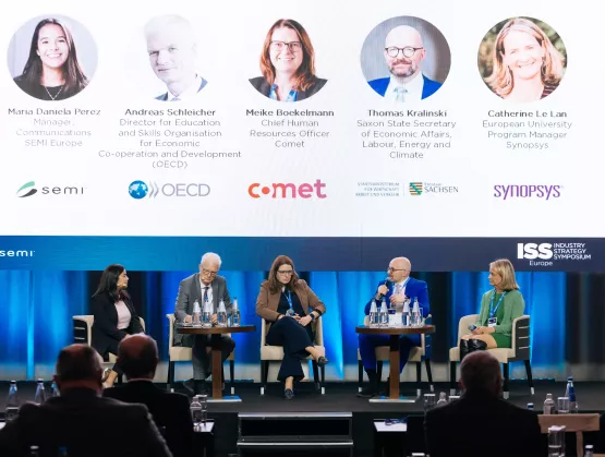
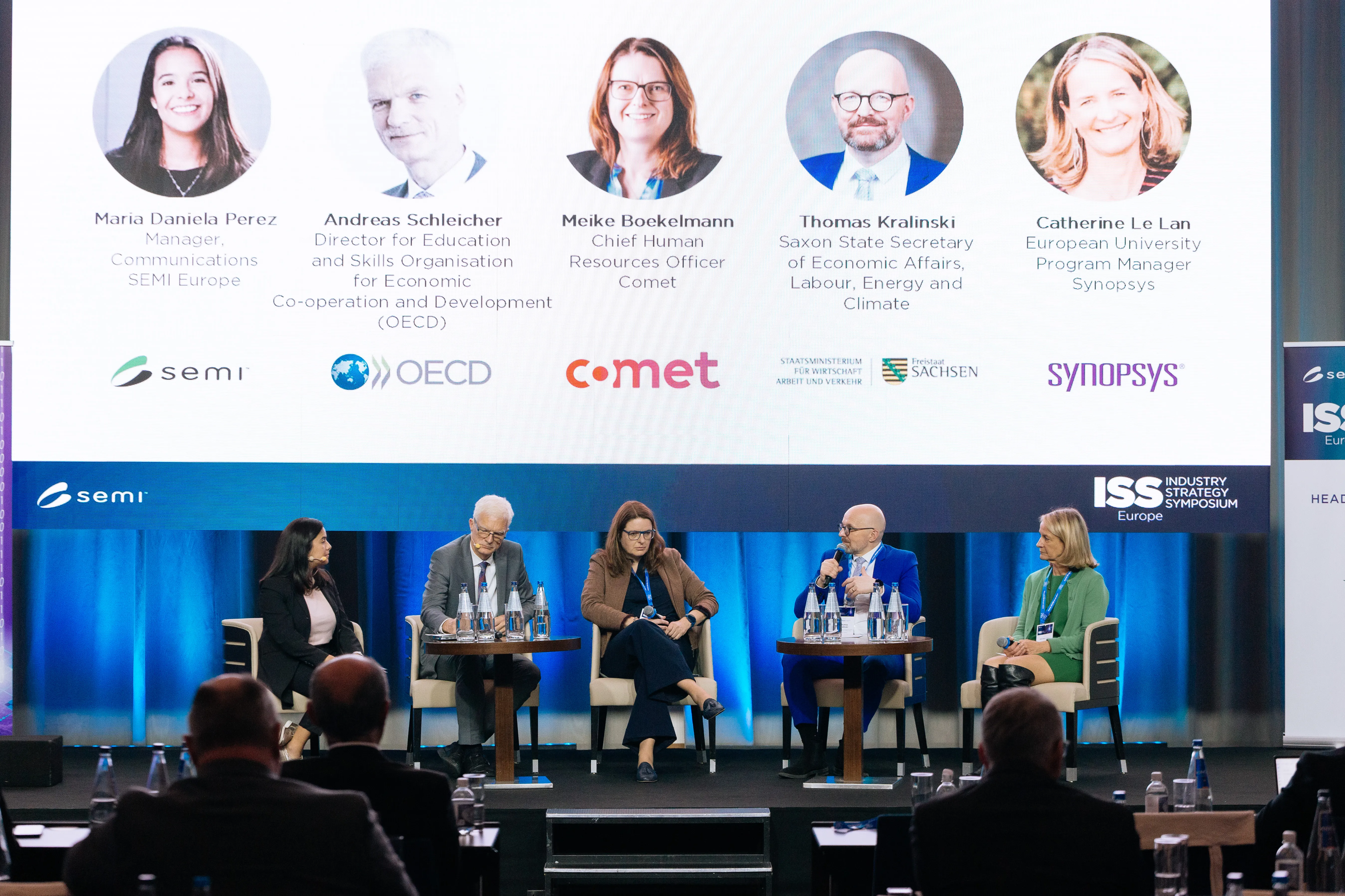
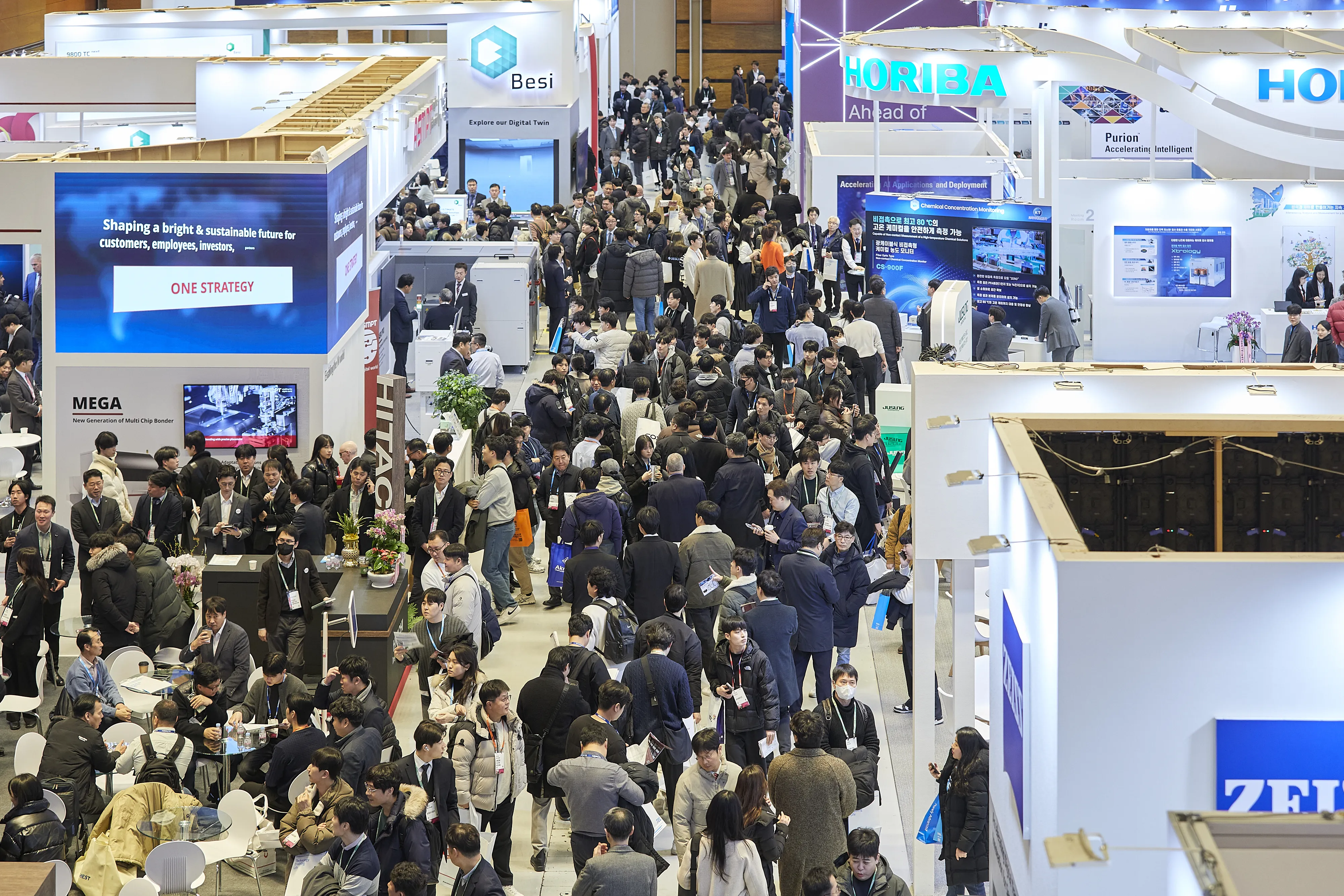
Geopolitical shifts, rapid technological advancement, and supply chain pressures continue to redefine the global semiconductor landscape. These forces framed the discussions at the 2025 SEMI Industry Strategy Symposium Europe (ISS Europe), held in Sopot, Poland. Over two days, industry leaders, and policymakers examined how Europe can boost resilience amid growing uncertainty.Artificial intelligence (AI) stood out as a key driver—powering global chip demand and transforming industry operations. In the past year, AI applications like generative models and edge computing helped push chip sales to new highs. The EU Chips Act, effective since September 2023, also fueled change. It has drawn tens of billions of euros into European semiconductor infrastructure, including major investments in Pomerania, the host region for this year’s symposium. “With AI expected to drive exponential growth in the semiconductor industry—projected to reach $1 trillion by 2030—Europe must act collectively to remain competitive,” said Laith Altimime, President of SEMI Europe. “We encourage collaboration across all countries to strengthen supply chain resilience, mitigate geopolitical risks, and harness the full potential of our diverse talent base.”Laith Altimime, President, SEMI EuropeSo what has the EU’s investment in the semiconductor industry achieved, and how much more remains to be done? Gustav Kalbe, Acting Director of Enabling and Emerging Technologies at the European Commission, cited €80 billion in public and private investment in European fabs as clear progress toward introducing "advanced technology that has not before been deployed on the continent of Europe." However, Kalbe emphasized a new urgency driven by AI’s rise. “We need in Europe a secure supply chain for AI chips in key sectors—particularly automotive,” said Kalbe. “That’s why we are really pushing for accelerated development of AI chips here.”Gustav Kalbe, Acting Director of Enabling and emerging technologies,DG CNECT, European CommissionPoland is a prime example of the EU Chips Act’s impact—driven by consistent government support. Dariusz Standerski, Secretary of State in the Ministry of Digital Affairs, highlighted Poland’s seven-pillar national semiconductor strategy, which includes expanding infrastructure and increasing engineering talent by 20% by 2030. “We need to build our production capacity to meet the strategic needs of Poland,” said Standerski. “Semiconductors are important not only because of market size, but because of their role in national security.”Dariusz Standerski, Secretary of State, Ministry of Digital Affairs, PolandRisks to the Industry from a World in Political TurmoilGeopolitical shifts and market volatility dominated the opening session of ISS Europe 2025. Malcolm Penn, CEO of Future Horizons, warned that despite strong 2024 revenues, industry fundamentals remain fragile. “All of the growth is in graphics processing units (GPUs) for AI and high-bandwidth memory (HBM) for AI servers—every other product sector is currently in recession,” said Penn. He forecast 12% industry growth in 2025 but cautioned against overcapacity and price pressures from China. “We are not seeing unit growth, and without unit growth, you don’t have sustainable market growth,” explained Penn. “If momentum in AI slows, the industry could face a significant retrenchment.”Malcolm Penn, CEO of Future HorizonsLooking beyond the immediate outlook for semiconductors, Hendrik Bourgeois, Vice President for European Governmental Affairs at Intel, turned the spotlight onbroader economic and security challenges facing the region. Bourgeois outlined four strategic policy priorities for Europe: Build internal strength to ensure external (global) relevance;Deepen alliances beyond the United States—such as with the UK, Canada, Japan, and South Korea;Be open to a stronger economic relationship with China;Recognize that the U.S. is more than its federal government: states, cities, people and corporations all have a role to play in bringing stability and certainty.Hendrik Bourgeois, Vice President for European Governmental Affairs, IntelBenedikt Ernst, Senior Vice President and Head of Strategy Transformation at Merck KGaA, Darmstadt, Germany, emphasized the strategic importance of strengthening Europe’s domestic semiconductor ecosystem. “No country or region can be fully self-sufficient,” said Ernst. “But Europe is particularly strong in domains like advanced materials, fabrication equipment, and semiconductor manufacturing. We have leading players in these fields – let’s bet on them.”Benedikt Ernst, Senior Vice President and Head of Strategy Transformation, Merck KGaA, Darmstadt, GermanyMikolaj Trunin, Deputy Director of the Invest in Pomerania, and its Strategic Investment Manager Radoslaw Bojarczuk, highlighted the region’s rising profile among global investors. Despite a global downturn in foreign direct investment (FDI) since 2015, the region stretching from Gdansk and Warsaw to Dresden and Magdeburg is emerging as a vibrant semiconductor hub. “The environment is becoming increasingly attractive to outside investors drawn by the region’s large talent pool, robust venture capital activity, and strong and stable economic growth,” said Trunin.Left: Mikołaj Trunin, Deputy Director, Invest in PomeraniaRight: Radosław Bojarczuk, Strategic Investment Manager, Invest in PomeraniaAdvancing on the Roadmap to Net ZeroThe symposium’s second session tackled sustainability—how to grow the industry beyond $1 trillion in revenue while cutting emissions. AI emerged as a key enabler of sustainable innovation. Bill Lussier, Managing Director of Tokyo Electron Europe, highlighted recycled aluminum which has a much lower carbon footprint, but noted that semiconductor equipment requires ultra-pure aluminum, which is not available off-the-shelf in recycled form. “The solution is to create a new circular economy for ultra-pure aluminum—a supply chain so complex that it cannot be managed without the aid of AI,” explained Lussier.Bill Lussier, Managing Director, Tokyo Electron EuropeAI is also helping decarbonize logistics, a critical yet often overlooked part of the semiconductor ecosystem. Rainer Kiefer, Executive Vice President and Global Head of Sales at Schenker AG, underscored the environmental cost of air cargo: “We need smart supply chain design to reduce the air miles of chips.” AI supports this by optimizing routing, loads, predictive maintenance, and demand forecasting. Rainer Kiefer, Executive Vice President and Global Head of Sales, Schenker AGHowever, AI brings new energy demands. Malgorzata Kasperska, Vice President of Secure Power at Schneider Electric, urged greater efficiency in AI data centers: “We need to optimize both power capacity and efficiency, and deploy high-density infrastructure, all while enhancing sustainability practices.” Malgorzata Kasperska, Vice President of Secure Power, Schneider ElectricEnergy-intensive fab operations remain a major challenge. Charles Vaillant, Chief Technology Officer at MANN+HUMMEL, noted that heating and ventilation account for up to 50% of a fab’s energy use. To improve efficiency, the company introduced a filtration system using activated carbon ceramic technology. The innovation reduces pressure drop, cutting fan energy use and delivering up to 41% energy savings in cleanroom environments.Charles Vaillant, Chief Technology Officer at MANN+HUMMELFinding the Talent to Fuel the Industry’s GrowthAttracting and developing talent remains a critical challenge for the semiconductor industry. Andreas Schleicher, Director for Education and Skills at the OECD, cited a visibility gap: “Young people don’t see these engineering and IT jobs. You cannot be what you do not see.” Meike Boekelmann, Chief Human Resources Officer at Comet, echoed the sentiment. “Face-to-face, we can get people excited about joining our industry,” said Boekelmann. “The challenge is getting them in front of us in the first place.” Andreas Schleicher, Director for Education and Skills,Organization for Economic Co-operation and Development (OECD)In a panel discussion on Bridging the Talent Gap for Sustainable Growth, moderated by SEMI Europe’s Maria Daniela Perez, speakers explored how industry and academia can better collaborate to meet evolving workforce demands. Thomas Kralinski, Saxon State Secretary of Economic Affairs, Labor, Energy and Climate, emphasized the importance of future-ready education. “Do we know which fab is going to be built in 2035, or which start-up will be founded? No—but all the people who will work there are already alive. We need education to prepare these people for this unknown future.Thomas Kralinski, Saxon State Secretary of Economic Affairs, Labor, Energy and ClimatePanel Discussion on Bridging the Talent Gap for Sustainable GrowthAI Intensifies Scale of Innovation in Semiconductor FabricationDay two of ISS Europe 2025 spotlighted AI’s transformative impact on semiconductor innovation, from materials to manufacturing and chip design. John Behnke, General Manager for Smart Manufacturing at INFICON, emphasized AI’s growing role in managing fab complexity. “You need a lot of highly knowledgeable people to run a fab today,” said Behnke. “They must analyze huge amounts of data, and balance priorities like quality, on-time delivery, cycle time, and profitability.” In the future, he explained, AI-powered optimization engines will shoulder that burden by making autonomous decisions.John Behnke, General Manager for Smart Manufacturing, INFICONJean-Christophe Eloy, CEO of Yole Group, pointed to the rapid growth of data centers as a catalyst for architectural transformation, predicting a shift from monolithic AI ASICs to chiplet-based designs. “In the future, we can expect to see much of the value in the semiconductor business transfer from the front-end chip to the advanced packaging that integrates chiplets,” said Eloy. Jean-Christophe Eloy, CEO, Yole GroupThis sentiment was echoed by Christophe Frey, Vice President of EU Engagement at Arm, who described the industry’s shift from systems-on-chip to systems-of-chips. “Chiplets represents a unique opportunity for Europe to re-enter the game of high-end chips,” said Frey. He emphasized the need for an open chiplet marketplace, an effort Arm supports, but warned, “There is a long road ahead of us,” citing the need for silicon qualification, profiling, test and debug infrastructure, software standards, and specifications for mechanical and thermal integration.Christophe Frey, Vice President of EU Engagement, ArmThat transition is already taking shape in manufacturing. Volker Herbig, Vice President of the Microsystems Business Unit at X-FAB, noted that capabilities developed for CMOS+MEMS sensor in the early 2000s are now enabling heterogeneous integration (HI) at scale. “We are now an open HI foundry,” said Herbig, adding that X-FAB is building a dedicated HI facility with support from the EU Chips Act. “This technology is propagating down from the high-performance computing (HPC) world to medical and industrial applications — It’s happening as we speak.”An Industry Changing Faster Than Ever Volker Herbig captured the industry’s rapid evolution with the “Red Queen” theory from Alice in Wonderland: “You need to run as fast as you can just to stay in the same place.”Volker Herbig, Vice-President, BU MEMS, X-FABClosing the symposium, Leonard Hobbs, Director for Government Affairs at Intel Ireland, cited Charles Darwin: “The species which can best adapt to changes in its environment is the one which survives,” Hobbs added, “Over the past two days we have learned much that can help Europe’s semiconductor industry to adapt successfully to a rapidly changed world.” Leonard Hobbs, Director for Government Affairs, Intel IrelandAt the symposium’s gala dinner, delegates celebrated leaders driving the industry forward. SEMI presented the 2024 SEMI European Award to Kurt Sievers, President and CEO of NXP Semiconductors, and honored Anna-Riikka Vuorikari-Antikainen, Chief Commercial Officer of Okmetic, with the Special Service Award.Kurt Sievers, President and CEO, NXP Semiconductors (Middle)Anna-Riikka Vuorikari-Antikainen, Chief Commercial Officer, OkmeticOn behalf of SEMI, the SEMI Europe team and ISS Europe committee would like to thank all speakers, sponsors, and attendees for making the event a great success.SEMI Contact Cassandra Melvin, Senior Director of Business Development and Operations Email: [email protected]
Read More
On April 8-9, 2025, bees on cherry blossoms lining the streets of Washington D.C. were not the only things buzzing. The word “tariffs” floated in the air from TVs and conversations throughout Capitol Hill, as people eagerly awaited the implementation and response to United States President Donald Trump’s latest round of far-reaching trade policy. This was the backdrop for this year’s SEMI Washington Fly-In, hosted annually by the SEMI North America Advisory Board (NAAB), which gathered representatives from member companies to meet with government officials and advocate for policy changes vital to the semiconductor industry’s continued growth and innovation.SEMI executives and more than 50 representatives from member companies across the end-to-end semiconductor supply chain participated in the Fly-In. SEMI President and CEO Ajit Manocha, SEMI Americas President Joe Stockunas, and SEMI Vice President of Global Advocacy and Public Policy John Cooney met with Trump administration officials from the Department of Commerce. Reflecting the global reach of SEMI, Manocha traveled from Washington to Brussels for meetings with the European Commission. On April 8, Stockunas presided over a NAAB meeting, followed by a dinner and prep session for meetings with Congressional members and their staff the following day. Building on the priorities outlined in the briefing book prepared by Cooney’s Advocacy team in Washington, participants discussed priority messages to convey tailored to the specific officials.Focus topics included:Tariffs and Trade – Address the buzz of the day’s news cycle by spotlighting the challenges of multiple layers of tariffs facing U.S. operations due to the industry’s global supply chain.Export Control Policy – Revise export control rules to be narrow and focused with increased transparency to minimize uncertainty for companies contributing to the world’s most complex manufacturing processes.Tax Policy and Investment Incentives – Extend tax credits set to expire and expand them to include semiconductor material suppliers and packaging facilities to bolster the full semiconductor ecosystem.CHIPS Act Implementation – Streamline implementation and ensure that the full intended scope of the CHIPS Act is maintained to meet the goals of the bipartisan legislation.Workforce Development and Immigration – Highlight the need for multi-layered programs – from education to apprenticeships through career development – required to provide the skilled workforce that will underpin domestic industry expansion.Energy and Environment – Showcase the need for strong R D programs, industry-led standards, and permitting reforms to help the semiconductor industry address booming energy requirements to power Artificial Intelligence and meet the resource needs of the growing domestic chipmaking ecosystem.PFAS Regulation and R D Needs – Prioritize regulatory actions that take a risk-based approach to PFAS and other chemicals critical to semiconductor manufacturing, as well as R D to improve environmental controls and identify potential alternative substances.SEMI organized four groups by U.S. region – East, Midwest/South, Southwest and West – comprised of representatives from member companies with operations in the respective states of the Senate and House of Representative offices scheduled for meetings at Capitol Hill. On April 9, the groups met with Members of Congress and their staff from 20 of the nation’s states, including Arizona, Arkansas, California, Colorado, Delaware, Idaho, Kentucky, Louisiana, Massachusetts, Michigan, Minnesota, New Mexico, North Carolina, Ohio, Oregon, Texas, Utah, Virgina, Washington and West Virginia. The groups shared powerful perspectives, data and anecdotes on the impact of policies on their companies’ operations. While the groups for the SEMI Washington Fly-In included representatives from companies that are fierce business rivals, the focus of the discussions successfully presented a unified industry voice highlighting shared challenges, policy recommendations, and request for support – in true SEMI “Stronger Together” spirit.News of a 90-day pause on most tariffs broke while the groups were conducting their meetings. The intense difficulties of tracking changes on tariffs and other policies permeated throughout the conversations on the impact on business decision-making. While influencing policy changes will not occur instantaneously, the SEMI Washington Fly-In bolstered the SEMI Global Advocacy team’s ongoing efforts to educate officials on the nuances and critical importance of the complete semiconductor supply chain. Additionally, the discussions emphasized the policy modifications that will have the greatest impact in helping the industry continue its lasting legacy of innovation that improves the quality of life for people in the U.S. and around the world.On April 11, the Customs and Border Patrol issued an addendum to the tariff exemption list that did not result in a complete exemption for the semiconductor supply chain. President Trump posted afterward on social media: "We are taking a look at Semiconductors and the WHOLE ELECTRONICS SUPPLY CHAIN in the upcoming National Security Tariff Investigations."Traditionally, such investigations have been conducted over a prolonged period of time for the government to collect data directly from companies and solicit feedback from industry. If past precedent remains, this will represent the first formal opportunity for industry to engage on the Administration's tariffs. The President has stated that his plans for tariffs on semiconductors will be unveiled this week.Visit SEMI Global Advocacy to learn more about public policy efforts and developments, and SEMI Workforce Development for more information on efforts to address the microelectronics industry’s talent needs.Samer Bahou is Director of Marketing Communications at SEMI.
Read More
The semiconductor industry is a rapidly expanding sector in the United States with an anticipated 115,000 new jobs by 2030. A projected 67,000 of these in-demand roles will remain unfilled (SIA Workforce Blueprint, 2024), given the current training landscape. To address this workforce challenge, many strategies must be leveraged. One solution is to diversify the education and training needed to move workers into the semiconductor industry. Through semiconductor-specific programming at community colleges and universities, institutions can attract a wide array of learners, and by creating flexible credit, non-credit, degree, diploma, and certificate programs, education providers can meet hiring needs through many pathways. The SEMI Foundation, the workforce development arm of SEMI, is now offering Fundamental Semiconductor Knowledge Certification for high-quality programs that prepare entry-level workers for success in the growing semiconductor industry. SEMI’s Fundamental Semiconductor Knowledge Certification conveys that: Learners who are new to the semiconductor industry and successfully complete the program will be well-prepared for entry-level roles; Program completers have had exposure to fundamental semiconductor industry information and context, as well as introductory hands-on experience;Completers of these programs will have the specific knowledge and skills required for entry level positions; andProgrammatic design and content have been informed through input and feedback from local industry partners.Certified Programs: Spotlight on Austin Community CollegeAustin Community College District (ACC)—located in Austin, TX, was the inaugural recipient of the SEMI Foundation’s Fundamental Semiconductor Knowledge Certification for their Advanced Manufacturing Production (AMP) program. The strength of ACC’s programming is further illustrated by the College’s partnership with America’s Frontier Fund (AFF) Foundation, Merit America, and the Texas Institute for Electronics to expand the AMP program across the United States in 2025. This expansion will allow job seekers to access the SEMI Certified AMP program in a flexible, location-diverse capacity. ACC’s Dr. Laura Marmolejo, Dean of Advanced Manufacturing, and Laura Lucas, Director of Strategic Initiatives, spoke with SEMI Foundation to share the origin story of AMP and provide lessons learned and advice for others who are developing or expanding similar programs. Dr. Laura Marmolejo, Dean of Advanced Manufacturing, and Laura Lucas, Director of Strategic InitiativesKnowledge Sharing: Best Practices and StrategiesWhen asked what other schools can learn from ACC's experience, Dr. Marmolejo and Ms. Lucas focused on three key areas: direct engagement with industry, flexibility on programming and meeting local needs, and developing a pathway that can be clearly communicated to learners and industry alike. Dr. Marmolejo emphasized the importance of developing strong connections with industry. “Start by building these relationships with the company. They need to trust you,” said Dr. Marmolejo.” Ms. Lucas also spoke of how the program's origin and ultimate success emerged from direct engagement with companies. By understanding direct needs at each company, identifying consistent needs between the companies, and identifying ways that the College could support those needs, ACC was able to offer multiple solutions that appealed to both students and employers. Austin Community College offers several ways for learners or jobseekers to deepen their knowledge of the semiconductor industry and advanced manufacturing sector. Learners can begin their journey with the College’s 8-week Advanced Manufacturing Production (AMP) program, upskill with the Core Automation Semiconductor Training (CAST) program, or pursue a bachelor's or associate degree.Another benefit of the close collaboration between ACC and industry is that the College "is understanding where the regional hiring demand is at any given time,” said Ms. Lucas. This awareness, coupled with a mindset of flexibility and adaptability among the instructors and administrators, allows ACC to align programming with local needs, ensuring that jobseekers experience success once they complete their programs. For example, recently in Austin, employers have been focused on upskilling existing employees, so ACC has been able to open more sections of the Semiconductor Technician Advanced Rapid Start (STARS) program for incumbent workers within the local workforce ecosystem. When hiring gaps require more new additions to the industry, ACC will be able to pivot to increased AMP and CAST programming. This awareness of industry needs and the flexibility allows ACC to think about its offerings holistically.Advanced manufacturing students at ACCAnother consideration that schools and faculty can keep in mind when developing programs is how they scaffold programming and communicate the pathways and differences between offerings to external audiences. Internally, the distinctions between programs may feel obvious, but learning how to promote each pathway to learners, and how to differentiate them when seeking employer input is critical. Whether it's AMP, CAST, or STARS, "the topics are the same; what’s different is the level of depth,” explained Dr. Marmolejo. Ensuring learners enroll in the right program for their individual needs and career path will help the College build the right pathways for students from education to career. Clear communication about programming will also inform the industry about the best ways to get and stay involved in course development and iteration. Dr. Marmolejo with advanced manufacturing students at ACCACC’s success in building pathways for students into industry at the local level is evident in the more than 2,800 students enrolled across all advanced manufacturing programs, as well as its upcoming national program expansion for AMP. Other educational institutions and training providers can learn from the best practices and experiences of ACC, and can similarly have their work reviewed and certified by the SEMI Foundation.Press event at ACC in November 2024 to announce the expansion of AMP program nationwide and the awarding of the SEMI Certification.SEMI Certification: Next Steps for Training and Education PartnersSEMI Certification for training programs communicates to learners, jobseekers, and employers that the awarded programs have achieved the highest standards of program excellence in preparing entry-level workers to succeed in the growing semiconductor industry. Through 2025, the SEMI Foundation plans to expand program and course certification to include technician training programs. If you are a training or education partner looking to submit a program for consideration, please complete the SEMI Certificate Screening form. For more information about existing and future SEMI Certification efforts, please contact Anissa Hamdon-Morison at [email protected] or visit SEMI Certified Programs Courses | SCAN.Anissa Hamdon-Morison is the Curriculum and Training Manager at the SEMI Foundation.
Read More
Insights from the ISS Europe 2025 Press Briefing in SopotAt the SEMI Industry Strategy Symposium Europe (ISS Europe) 2025, held in Sopot, Poland, senior leaders from government, industry, and the investment community came together to share insights on Europe’s evolving semiconductor landscape. During a dedicated press briefing, they addressed Poland’s growing role in the ecosystem, the significance of international collaboration, and the strategic levers needed to bolster Europe’s competitiveness in semiconductors.Against the backdrop of accelerating investment through the EU Chips Act, speakers emphasized that building Europe’s semiconductor future will require more than funding. It will demand cross-border collaboration, cohesive public-private strategies, and a long-term vision to ensure talent pipelines and supply chain resilience.The briefing featured remarks and commentary from:Laith Altimime, President, SEMI EuropeAgnieszka Sygitowicz, President, The Polish-Taiwanese Chamber of Commerce and IndustryPawel Pudlowski, Ph.D., Deputy CEO, Polish Investment and Trade Agency (PAIH)Monika Morali-Majkut, Chairwoman of the Supervisory Board, Atlas WardBenedikt Ernst, Senior Vice President and Head of Strategy Transformation, Merck KGaA, Darmstadt, GermanyDionys van de Ven, President, Comet YxlonAnna-Riikka Vuorikari-Antikainen, Chief Commercial Officer, Okmetic From left to right: Agnieszka Sygitowicz, President, The Polish-Taiwanese Chamber of Commerce and Industry; Pawel Pudlowski, Ph.D., Deputy CEO, Polish Investment and Trade Agency; Monika Morali-Majkut, Chairwoman of the Supervisory Board, Atlas Ward; Laith Altimime, President, SEMI Europe; Benedikt Ernst, Senior Vice President and Head of Strategy Transformation, Merck KGaA, Darmstadt, Germany; Dionys van de Ven, President, Comet Yxlon; Anna-Riikka Vuorikari-Antikainen, Chief Commercial Officer, OkmeticSEMI: How are the private sector and international partners contributing to Poland’s ecosystem development?Morali-Majkut: The private sector is essential to building Poland’s semiconductor ecosystem. At Atlas Ward, together with like-minded companies, we’ve launched SEMICON Supply Poland to help develop a strong, scalable supply chain. We’re working to ensure that essential infrastructure is ready: land, utilities, materials, and specialized service providers that can meet the needs of incoming semiconductor investments. But this isn’t just a national effort. We’re closely aligned with ecosystem-building in Dresden, Prague, and across Central Europe. Collaboration across borders is essential.Sygitowicz: We believe strongly in the philosophy of “building bridges.” In our work with Taiwan and other partners, we focus on five “bridges”: knowledge, people, business, development, and shared success. These connections are critical for Poland to become an integral part of the global semiconductor supply chain. Poland is not trying to replicate what others have done, but to learn from it—particularly in ecosystem development. The long game is not just investment attraction; it’s ecosystem maturity. SEMI: Talent shortages remain a major concern across the industry. What steps are being taken to prepare the future-ready workforce?Morali-Majkut: We are working closely with academia to build the talent pipeline Poland will need as its semiconductor sector grows. Together with industry partners, we’re developing vocational training programs and university-level collaborations aimed at aligning skills with industry needs. There are already several R D-focused projects underway at Polish technical universities, and Poland’s strong foundation in technical education positions us well to support workforce growth as the industry scales up.The semiconductor industry has one of the most complex supply chains in the world. Investing in this industry creates ripple effects across a wide range of skill areas. When we invest in semiconductor education, the spillover benefits for the broader economy will be immense.Altimime: While the talent shortage is certainly a challenge, it also presents a massive opportunity. At SEMI, we’re committed to making Europe’s semiconductor investment a long-term success. Through strong collaboration with the European Commission and a broad network of consortium partners across Europe, including Poland and other Eastern European countries, we’re pushing forward both public and private sector engagement to ensure the continuity of growth and innovation.Europe is projected to face a shortage of 271,000 skilled workers in the semiconductor sector by 2030 if current trends persist. To address this challenge, SEMI is leading a range of initiatives focused on reskilling, upskilling, and cross-sector knowledge development. We’ve established an Educational Leaders Board with 18 consortium members and are organizing events to reach out to students and educational institutions – including the recent SEMI On Campus with the University of Gdańsk — all to foster stronger connections between academia and industry. SEMI: How can Europe strengthen its semiconductor supply chain resilience in the face of geopolitical challenges?Ernst: Resilience starts with recognizing and building on Europe’s existing strengths. While much attention is often given to gaps, Europe already has world-class players, technologies, and a strong consumer market. These are key strategic assets. What’s needed now is coordination—government and industry must work together to align efforts, avoid fragmentation, and ensure that political initiatives channel support in a unified direction.Van de Ven: For industry, true resilience means the freedom to operate globally. Trade controls and IP restrictions can create bottlenecks, so policies must support open access to markets across regions—including the U.S., Europe, and Asia. Companies also need to co-create with fabs and universities, embedding themselves where talent is trained and where innovation happens. This creates a robust, future-ready ecosystem. Location decisions are increasingly influenced by proximity to both production facilities and research institutions.Sygitowicz: Poland is well-positioned to support investment through a combination of ready-to-develop land, financial incentives (such as grants and tax exemptions), and ecosystem services. Beyond infrastructure, there is growing government support for talent development and innovation. Startups, accelerators, and academic partnerships are playing a larger role in building the technology pipeline—creating a more comprehensive, innovation-friendly environment for foreign investors.Vuorikari-Antikainen: Speed is an often overlooked but critical factor in competitiveness. Europe has historically moved slowly, but if countries like Poland can create fast-track pathways for permitting, investment, and project execution, they can set themselves apart. Pairing this agility with strong education and startup ecosystems will help deliver long-term resilience and responsiveness to market needs.Altimime: We must avoid country-centric thinking. Europe’s strength lies in its diversity with different regions excel in different areas, and the challenge is to bring those strengths together. Initiatives like the pilot lines are a great example of this in action, connecting capabilities in photonics, advanced packaging, and quantum technologies across the continent. With strong leadership from Europe’s research and technology organizations (RTOs), such as the Technical Research Centre of Finland (VTT), we’re seeing renewed momentum in areas where Europe has historically been strong, like communications and photonics.To truly accelerate Europe’s position in the global semiconductor landscape, we need to focus on integration—connecting the dots between regions, institutions, and industries. From left to right: Laith Altimime, President, SEMI Europe; Benedikt Ernst, Senior Vice President and Head of Strategy Transformation, Merck KGaA, Darmstadt, Germany; Dionys van de Ven, President, Comet Yxlon; Anna-Riikka Vuorikari-Antikainen, Chief Commercial Officer, OkmeticSEMI: With the European Commission discussing a potential second Chips Act, what lessons should we carry forward from the first—and how can Poland play a stronger role?Van de Ven: The primary objective of the Chips Act should be to enable investment and industrial action. In some cases, we’ve seen frameworks become overly complex, attempting to define platforms or outcomes in ways that don’t always align with business needs. From an industry standpoint, what’s most helpful is straightforward support—mechanisms that empower companies to invest where it makes sense and move quickly. Ultimately, the private sector will determine how to build and scale the necessary infrastructure and innovation.Pudlowski: It’s true that Poland did not benefit from the first Chips Act to the extent that its assets and potential might suggest. We offer a combination of engineering talent, geographic advantage, and industrial readiness—yet, in terms of EU-level influence and visibility, we’ve been underrepresented. That is beginning to change.Poland now has a national semiconductor strategy backed by the government, and this, combined with growing engagement from organizations like SEMI, positions us for stronger inclusion going forward. At the same time, we need more bottom-up visibility. Companies in Poland should proactively present their capabilities and publish their work more widely. We have a great deal to offer, and now is the time to ensure that’s recognized in Brussels and across Europe.Altimime: Poland’s recent release of its national chip strategy is both timely and critical. From SEMI’s perspective, this is a proven model: a clear strategic roadmap, strong government backing, and industry alignment create the right environment for success. The first Chips Act delivered real progress and global attention, and with Poland’s new strategy in place, we expect to see even greater integration into the European semiconductor value chain in the next phase of the initiative.Morali-Majkut: During recent conversations with international partners, particularly in Asia, it became clear that while countries like Germany and the Czech Republic are well known within the semiconductor ecosystem, Poland has not always been equally visible—despite being geographically and industrially well-positioned. That perception is starting to shift.Poland has long played a vital role in Europe’s industrial supply chain, particularly in collaboration with Germany. We bring a strong foundation in engineering, education, cost-efficiency, and industrial land availability. These assets are highly relevant to semiconductor expansion. Rather than seeing countries in isolation, we should frame this as a collaborative regional model—linking Germany, the Czech Republic, and Poland as an integrated supply chain hub. SEMI ContactSitong He, Communications ManagerEmail: [email protected]
Read More
The semiconductor industry lies at the heart of Europe’s technological ambitions, powering breakthroughs in artificial intelligence, quantum computing, and advanced manufacturing. However, as the industry expands rapidly to meet surging global demand, the need for highly skilled workers is outpacing supply. According to the recently published ECSA Skills Strategy, Europe must train and hire tens of thousands of skilled professionals by 2030 to remain globally competitive. Without a robust and inclusive talent pipeline, the region’s independence in critical technologies might be at risk.At this year’s Industry Strategy Symposium Europe (ISS Europe) held in March, a panel discussion moderated by Maria Daniela Perez from SEMI Europe, brought together industry leaders and experts to explore solutions to this challenge. The discussion centered on how emerging technologies are reshaping the workforce, the role of education in preparing future professionals, and strategies for attracting and retaining diverse talent – all critical to ensuring sustainable workforce development in the semiconductor industry.Tackling Talent Acquisition and RetentionCatherine Le Lan, European University Program Manager from Synopsys, drew a direct connection between technological disruption and workforce challenges. “AI is driving unprecedented changes, and hardware is at the heart of the AI revolution,” said Le Lan. As the industry invests in new methodologies, leading-edge technologies, and innovative products, the demand for updated skillsets continues to outpace supply. This places a dual burden on companies – who must hire for both today’s and tomorrow’s skills – and on the education sector, which is expected to rapidly adapt.Meike Boekelmann, Chief of Human Resources at Comet, highlighted that the challenge is not just about attracting talent from within the semiconductor field – it is also about standing out in a crowded talent market. “We are not only competing within our industry for talent. We’re also competing against other industries: automotive, consumer electronics, and AI,” said Boekelmann. To succeed, companies must go beyond traditional incentives and offer meaningful, forward-looking career experiences. “Primarily what I see is that they’re really asking for creating an impact and also a sense of belonging… so they want to see what’s the outcome,” she explained. “There are more people leaving the labor market than entering the labor market,” added Thomas Kralinski from the Saxon State Secretary of Economic Affairs, Labour, Energy and Climate. “We need to think about immigration, family-work integration, and training.” His comments underscore the need for a holistic workforce strategy – one that not only fills immediate vacancies, but also strengthens the broader ecosystem through inclusive policies, targeted reskilling, and long-term demographic planning.Fostering Industry-Academia SynergyAs the industry evolves, so must its workforce. Andreas Schleicher, Director for Education and Skills at the OECD, made a stark observation. “There’s one thing worse than losing people – and that is to keep them and not upskill them.” He warned that the current pace of technological change demands far more than one-time training; it requires a culture of continuous learning. “Neither the industry nor the education sector has the capacity for upskilling and reskilling,” he noted, pointing out that while Europe performs well in early education, adult learning remains insufficient. “The incidence and intensity of upskilling and reskilling is so far out of what we will need.” Without scalable, lifelong learning systems, even experienced professionals risk being left behind.Building on this idea of future-readiness, Thomas Kralinski noted: “Do you know what kind of fab is going to be open in 10 years’ time or what startup is going to be founded in 10 years’ time? You probably don’t. But everybody who’s working there or will work there is born already – and is probably in school or at the university.” He underscored the need for steady investment in teachers, training systems, and educational infrastructure – not just to meet today’s demand but to ensure Europe’s long-term competitiveness.To truly inspire the next generation, Schleicher pointed to visibility as a vital factor. “You cannot be what you cannot see.” Without relatable role models or a clear understanding of how their interests connect to meaningful careers, young people – especially underrepresented students – often overlook STEM pathways. Schleicher described how even small actions, like industry professionals visiting schools to explain their work, can have a lasting impact. “You can bring someone from the semiconductors industry to speak to students and help them understand, for example, what’s in a mobile phone and that they can actually create tomorrow’s mobile phone.” That kind of engagement, he argued, helps “build dreams” and makes technology tangible, exciting, and inclusive.AI: An Enabler, Not a ThreatPanel moderator Maria Daniela Perez raised a critical question about the evolving role of AI in the workforce. Acknowledging the widespread concern that AI could lead to job displacement, she challenged the panel to consider a different perspective. How can AI be leveraged to broaden and accelerate the talent pipeline rather than replace it? In response, the panelists emphasized that AI is not a disruptor but an accelerator. Rather than eliminating jobs, AI-driven tools enhance productivity by automating repetitive tasks, freeing professionals to focus on innovation, problem-solving, and high-value work. Catherine Le Lan provided a compelling example, explaining how AI-powered electronic design automation (EDA) tools are enabling engineers to push the boundaries of technological advancement. She referred to a university study that compared two groups of students – one with access to AI tools and one without. “They found out that those AI tools helped to improve productivity and also helped to improve skills of the students,” she said. “The student who had used AI tools had better skills than the one who hadn’t used AI tools… because they had been able to focus on the high-level skills, and they got rid of the low-level skills.” Her remarks underscored how AI, when integrated into education, can accelerate both efficiency and learning outcomes.Collaboration: The Key to Sustainable Workforce DevelopmentAddressing the workforce challenge requires cross-sector collaboration among industry, academia, and policymakers. There is a shared responsibility to invest in long-term education strategies, develop structured training initiatives, and create an ecosystem where talent can thrive. This is precisely the mission of two SEMI Europe-led initiatives.The European Chips Skills Academy (ECSA) and the European Chips Diversity Alliance (ECDA) are playing a critical role in shaping Europe’s semiconductor workforce. ECSA is driving efforts to align education and training with industry needs, ensuring that both students and professionals are equipped with the technical expertise and practical experience required for the sector’s future. Meanwhile, ECDA focuses on building a more inclusive semiconductor workforce across the industry. By creating opportunities for underrepresented groups, ECDA is ensuring that the industry benefits from a broad talent pool.Securing Europe’s Semiconductor FutureIn her closing remarks, Maria Daniela Perez brought the discussion full circle, emphasizing that addressing the semiconductor talent gap requires collective ownership: “In the end, it ends up being all about collaboration,” said Perez. From engaging technology users to amplifying the industry’s visibility, to aligning with academia and policymakers, the path forward depends on shared action. By fostering this ecosystem-wide commitment – and investing in the people behind the progress – Europe can bridge the talent gap and shape a resilient, inclusive, and globally competitive semiconductor workforce.SEMI ContactKartikey Srivastava, Senior Specialist, CommunicationsEmail: [email protected]
Read More
The SEMI Startups for Sustainable Semiconductors Program – or S3 – connects promising climate technology startups with many of the industry’s largest Corporate Venture Capital (CVC) firms. For startups interested in applying their solutions to improving sustainable practices within the semiconductor industry, the call for applications is open until May 1. After applications have been submitted, finalists will pitch their solutions to an audience at this year’s SEMICON West, taking place from October 7-9 in Phoenix, Arizona. Solutions of Interest – 2025 S3 Categories Each year, sponsors choose priority categories for sustainability-related solutions. This year’s categories include: Sustainable and efficient solutions for data centers, including thermal management, power management, and systems and componentsGenerative AI, software, and other AI solutions for alternative materials discovery, device and physics simulation, energy-efficient chip design, and end-to-end sustainable product designMore sustainable solutions for energy and materials, including new process designs for lower energy intensity, energy tracking and management software, emissions control and abatement, water solutions, PFAS destruction, and recycling solutionsAll startups that address any of these areas are encouraged to apply. Why Apply for S3?Startups that apply for S3 can benefit from the following. Mentorship from industry experts on how to break into the semiconductor industry, even if your startup had never previously considered the semiconductor market for its products or servicesProof of concept (POC) and pilot partnership opportunitiesExposure to major semiconductor industry leadersPotential investments from both CVCs and venture capitalists (VCs) throughout the program and final pitch eventAdditional public relations opportunities as a result of the programS3 Performance ReportTo help prepare for the 2025 competition, the S3 team conducted a review of the application process to develop a report card of key performance indicators. After assessing three years’ worth of data from over 150 startup teams, notable takeaways from the report are as follows. The S3 program provides startups with a 4.1% chance of securing a scaled customer. To date, S3 has enabled eight direct VC investments, 34 first-of-their-kind proof of concepts, and seven sustainability innovations that have scaled into initial production.One in three startups reviewed by internal subject matter experts moves into a POCOne in five startups that secure a POC move into a scaled deploymentOne in two startups that move into scaled deployment receive direct investment from the CVC arm of the companyApproximately one in 30 startups are successful at a first-scaled deployment with a semiconductor customerBy providing footholds into the semiconductor ecosystem through mentoring and customer introductions, S3 offers the opportunity for startups to strategically solve pressing, real-world technological challenges. Forward Statements To achieve a more sustainable semiconductor industry, we must move faster. The longer humanity takes to resolve unsustainable practices, the more expensive solutions will become. Through collaboration and competition, we can advance development on a larger, more efficient scale. To learn more, download the full report. John Wei joined Applied Ventures in 2020. He focuses on a range of deep tech areas and industry verticals, including advanced materials, display, and Industry 4.0 technologies. He also manages Applied Ventures’ investment activities in the Greater China region.Prior to joining Applied Ventures, Wei was a key member of the SABIC Ventures investment team, where he led multiple investments in advanced materials, display, energy sustainability, and manufacturing space in North America, Europe, and China. Earlier in his career, Wei held various commercial and technical roles at The Linde Group and General Electric with domain expertise in the petrochemical, power generation, alternative energy and oil gas industries.
Read More
SEMICON Korea 2025 held February 19-21 at the COEX in Seoul was the largest ever, covering 41,832 sqm, with 500 companies participating. Over the course of three days, 70,000 semiconductor professionals from around the world gathered to explore new partnerships, fostering industry growth and technological innovation. Thank you to everyone who participated in SEMICON Korea and helped make the event a success! SEMICON Korea 2025 Keynotes Call for CollaborationKeynote speeches featured leaders from AMD, Applied Materials, imec, Samsung Electronics and Synopsys, who shared their vision for the semiconductor industry.The speakers emphasized the importance of technological innovation in preparing for the AI era. They highlighted "collaboration" as the most crucial factor for achieving these innovations. "Co-Innovation Through Collaboration Across the Entire Semiconductor Supply Chain"Jaihyuk Song, CTO of Samsung Electronics, said, "Innovation for advanced semiconductor technology is no longer an issue that a single company can resolve alone. Close collaboration with equipment and materials companies, design companies, research firms, and universities is essential." He further emphasized, "Improving AI semiconductor performance goes beyond basic customer-supplier relationships; it demands a co-development system that seamlessly integrates front-end and back-end process collaborations.”"Independent Process Stages in Semiconductor Manufacturing Is Over"Prabu Raja, President of Applied Materials, remarked, "In the past, transistors, interconnects, and packaging were optimized separately, but now a change at one stage affects at least 100 subsequent processes, forming a highly complex structure." He explained that the semiconductor industry now requires an integrated approach from design to production rather than mere process optimization. Speed, optimization, and new methodologies will be key to creating the next semiconductor manufacturing paradigm.”"Independent R D Slows Down Innovation"Luc Van den hove, CEO of imec, pointed out, "Each major semiconductor region has its unique strengths, and attempting self-sufficiency in semiconductor manufacturing within a single region could face serious setbacks." He also shared that imec is actively collaborating with Korean semiconductor companies to develop ‘next-generation memory semiconductors.’AI was another hot topic that took center stage during the keynote presentations. "No AI Advancement Without Power Efficiency Innovation"Bill En, Corporate President of AMD, explained, "In the past, computing demand doubled regularly, but the introduction of large-scale AI models like ChatGPT has increased demand 20 times. As a result, the number of data centers has grown from 8,000 in 2021 to 10,655 in 2024, leading to exponential increases in power consumption." He emphasized, "Advancing AI requires power efficiency innovation, and the industry must go beyond hybrid bonding and gate all around (GAA) technology to develop new semiconductor manufacturing techniques.""AI Will Solve the Semiconductor Design Talent Shortage"Ravi Subramanian, Chief Product Management Officer of Synopsys, stated, "With AI development, chip design can now be conducted using AI, offering a solution to the talent shortage in semiconductor design."Additionally, Jaihyuk Song noted that AI is expected to evolve by mimicking the human brain, while Luc Van den hove pointed out that while GPUs are currently ideal for running large AI models, a more versatile chip architecture and technological platform are needed for future AI advancements.Fostering Collaboration at SEMICON Korea 2025To support the global expansion of Korean semiconductor equipment, materials and parts companies, the "Supplier Search Program" was also held during SEMICON Korea. This program invited major global players such as Applied Materials, GlobalFoundries, Kioxia, and Micron to connect and explore new business opportunities with over 100 Korean companies. Additionally, a "Leadership Dinner" was hosted to strengthen partnerships among global leaders. During this event, the SEMI Award ceremony was held to honor companies and individuals who have significantly contributed to the semiconductor industry's development. Congratulations to all the award winners!Leadership Dinner of SEMICON Korea 2025Market Trends Observed at SEMICON KoreaAccording to SEMI’s Senior Director, Clark Tseng, the semiconductor industry is expected to grow at a compound annual growth rate (CAGR) of 10% from 2023 to 2030, reaching a market size of $1 trillion by 2030.Semiconductor Market Outlook from Clark Tseng’s PresentationBoth Gartner’s VP Analyst, Gaurav Gupta and SEMI’s Clark Cheng identified AI as the key driver of this industry growth, with the automotive sector playing a crucial role in long-term expansion.Semiconductor Equipment Market Outlook by Regions from Clark Tseng’s PresentationThe outlook for semiconductor equipment, considered a leading indicator for the industry, also remains strong. The total semiconductor equipment market revenue is expected to reach $112.8 billion in 2024, $121.5 billion in 2025, and $139.4 billion in 2026. Korea’s semiconductor equipment investment is projected to rise from $19.7 billion last year to $23.4 billion this year and $29.2 billion next year. Meanwhile, China’s share of total investment is expected to decline from 43% in 2023 to 31% in 2024 and 28% in 2025.Special Programs at SEMICON KoreaIn addition to market forecasts and advanced technology conferences, SEMICON Korea 2025 featured 30 special programs on hot industry topics. The "Investment Forum" provided in-depth investment insights into the U.S. and Vietnam, while the first-ever "Netherlands-Korea Semiconductor R D Cooperation Seminar" was held to promote R D collaboration between Korea and the Netherlands. Notably, the Dutch Minister of Economic Affairs participated in this event.Dirk Beljaarts, The Netherlands Minister, Economic Affairs – Welcome Speech at the Netherlands-Korea Semiconductor R D Cooperation SeminarOther key conference topics included cybersecurity, compound power semiconductors, PFAS regulations, sustainability, and smart manufacturing.The Race to Secure Talent Was in Full Swing!At SEMICON Korea 2025, exhibitors actively operated recruitment sessions in their booths, with long queues of students eager to participate. Exhibitors increasingly use SEMICON Korea as a platform not only to showcase advanced semiconductor manufacturing solutions but also to attract future talent.This year, approximately 5,000 university students participated in SEMICON Korea. While many students registered individually, several universities also organized group visits, providing students with an opportunity to gain firsthand experience of the global semiconductor ecosystem.Special Talent Development Programs at SEMICON KoreaTo address the semiconductor industry’s talent shortage, SEMICON Korea hosted various talent development programs:Meet the Experts!: Engineers from Applied Materials, Entegris, Hitachi High-Tech, KLA. Lam Research, SEMES, TEL, Wonik IPS and YC mentored university students on career development.Women-in-Technology: Female leaders in advanced industries shared insights on promoting diversity in the semiconductor sector.Tutorials: Six basic level programs for semiconductor manufacturing technology were provided to strengthen the competitiveness of university students and junior engineers.The Path to Becoming a Semiconductor Equipment Specialist: Undergraduate students aspiring to become semiconductor equipment experts explored career paths alongside global professionals.Meet the Experts!Mark Your Calendar for SEMICON Korea 2026!SEMICON Korea 2026 will be held from Wednesday, February 11 to Friday, February 13, at COEX in Seoul. Don’t miss this opportunity to explore the cutting-edge technologies shaping the future of the semiconductor ecosystem!
Read More
The semiconductor industry is at a pivotal moment, with smart manufacturing, smart mobility and workforce development as key drivers in the industry’s path to reach $1 trillion in revenue by 2030. Bringing together key stakeholders from the semiconductor ecosystem, SEMIEXPO Heartland will take place on April 1-2, 2025, in Indianapolis and explore the latest advancements and opportunities to foster growth, accelerate innovation and reinforce the Midwest as a thriving hub for semiconductor manufacturing.SEMI sat down with Purdue University President Mung Chiang who shared his insights on growing semiconductor industry in the Midwest, how Purdue is making an impact, and a sneak peek into his upcoming keynote presentation at SEMIEXPO Heartland.SEMI: How important is semiconductor industry expansion in the Midwest?Chiang: Purdue’s partnerships with industry leaders, state and federal government are essential to advancing the U.S. semiconductor industry and establishing the Midwest region as the Silicon Heartland. The Department of Defense-funded Silicon Crossroads Microelectronics Commons innovation hub is a partnership between Indiana, Illinois, and Michigan, while the Midwest Microelectronics Network is in collaboration with Ohio, Illinois, and Michigan.An event like the SEMIEXPO Heartland in Indianapolis gathers industry representatives from across the nation to see the potential and value that Indiana and the Midwest bring and provides a great forum to explore strategies for collaboration and innovation.SEMI: How important is collaboration between industry and academia to advance semiconductor innovation and address workforce challenges?Chiang: Enabled by semiconductors, artificial intelligence (AI) continues to advance rapidly. Purdue is a national academic leader in microelectronics and semiconductors in part because of industry partnerships – both nationally and internationally – that help us align our research and workforce development to the needs of our industry partners.Collaborations among industry, academia and government will be critical to strengthening America’s position in the global semiconductor landscape and securing our technological future. Two recent examples are our partnership with SK hynix to fill a critical gap in the U.S. semiconductor supply chain and our partnership with SEMI, the leading global microelectronics industry association, to create online courses aimed at bolstering the semiconductor workforce.SEMI: How are Purdue’s innovations contributing to those fronts?Chiang: World-leading research, transformational investments in infrastructure and pioneering education are all part of Purdue’s contributions to advance the semiconductor industry.Strategic initiatives like the first comprehensive, large-scale Semiconductor Degrees Program, advised by a board of industry leaders, lead the way to high-quality workforce development at scale. Experiential education, such as programs like “Summer Training, Awareness, and Readiness for Semiconductors” (STARS) for undergrads, energizes first-year students and provides a strong foundation to prepare the next generation high-tech workforce, a critical step in cultivating the talent needed to drive the industry forward.Birck Nanotechnology Center, one of the nation’s state-of-the-art academic research centers, is another prime example of Purdue driving innovation. This facility will soon become the first and only digital-twin-enabled semiconductor research lab in the world.SEMI: What are the highlights of your keynote address for the SEMIEXPO Heartland?Chiang: I’ll point out that these are exciting times in Indiana – two new semiconductor clusters are emerging, one in West Lafayette at Purdue focused on the commercial sector and one at Westgate, near the Naval Surface Warfare Center Crane, focused on the defense sector.The initiative at Purdue is led by SK hynix, the world’s leader in high-bandwidth memory for AI; MediaTek, the world’s fifth-largest fabless design company and a leader in chips for smartphones, tablets, TVs, and Internet of Things products; and by imec, the world's leading independent semiconductor research and innovation hub.Our goal is to leverage Purdue’s excellence at scale to work with our partners and create a new, thriving, vibrant, and growing semiconductor hub in the heartland and to connect this growing commercial sector to the emerging defense sector at Westgate.We look forward to working with our partners in the Midwest to make the Heartland one of the few critical regions of semiconductor manufacturing, design, innovation, and talent development in the United States.SEMI: Part of SEMIEXPO Heartland’s focus is on smart manufacturing. What strategic collaborations in smart manufacturing are driving innovation forward?Chiang: Smart manufacturing is being driven, in part, by the continuing advancement of AI and digital twins. The semiconductor industry already is partnering with computational modeling and fabrication leaders like Purdue University to develop the digital twins and play a major role in training the workforce and accelerating the pace of innovation.The NIST-funded SMART USA Manufacturing Institute for Digital Twins is a $1 billion plus program that brings industry and academia together. Purdue looks forward to playing a leading role in this important initiative.Maintaining a strong connection between academia and industry can help accelerate design and innovation of new U.S. chip development and manufacturing concepts through cost reduction, product optimization and real-time process adjustments.ResourcesHear more from academic leaders, industry executives and government officials about the semiconductor expansion and opportunities for growth in the U.S. Midwest during SEMIEXPO Heartland event, April 1-2, 2025, in Indianapolis. Visit the SEMIEXPO Heartland website to view the full agenda: https://semiexpo.semi.org/.Mung ChiangMung Chiang is the President of Purdue University, and the Roscoe H. George Distinguished Professor of Electrical and Computer Engineering. Prior to being selected university president in 2022, he was the John A. Edwardson Dean of the College of Engineering and executive vice president for strategic initiatives at Purdue University.Chiang received BS (1999), MS (2000) and PhD (2003) from Stanford University and an honorary doctorate (2024) from Dartmouth College. Before 2017, Chiang was the Arthur LeGrand Doty Professor of Electrical Engineering and an affiliated faculty in Computer Science and in Applied Mathematics at Princeton University.SEMI ContactSherrie Gutierrez, Marketing Communications ManagerEmail: [email protected]
Read More