downloadGroupGroupnoun_press release_995423_000000 copyGroupnoun_Feed_96767_000000Group 19noun_pictures_1817522_000000Member company iconResource item iconStore item iconGroup 19Group 19noun_Photo_2085192_000000 Copynoun_presentation_2096081_000000Group 19Group Copy 7noun_webinar_692730_000000Path
Skip to main content
The semiconductor industry is at the forefront of technological innovation, with rapid advancements in recent years. As a result, the need for high-quality products and technologies has become increasingly important. To address this challenge, SEMI has launched the Quality Benchmarking Consortium (QBC), a new initiative dedicated to advancing quality best practices across the global semiconductor industry. Quality is a fundamental requirement for all semiconductor products and technologies. Over the past decade, state-of-the-art quality practices have evolved significantly to keep pace with rapid innovation and technological advancements. However, new challenges have emerged, including qualifying increasingly complex systems, advanced packaging and 2.5/3D integrated systems, and the growing role of AI/ML in manufacturing. Company-to-company benchmarking is a powerful tool for enhancing quality practices. By sharing information, input, and feedback, companies can establish best-known methods (BKMs) to elevate quality best practices across the entire industry. This approach can save time and money, while also driving innovation and improvement. The QBC is open to multinational corporations, including device manufacturers, fabless device makers, and foundries, that ship over 100 million units per year and have a high-caliber quality organization. The consortium operates on a "Give-to-Get" philosophy, requiring members to actively participate in discussions and activities. Permitted topics for discussion include working processes, management systems, approaches, and KPIs, driven by global customer trends or internal development. However, off-limit topics include IP and patent-protected quality technical solutions embedded in technologies, packages, design, testing, and software.Figure 1: (From Right to Left) - Georg Talut (Global Foundries), JensLuepke (Infineon), Rutger Wijburg (Infineon), Roberto Lissoni (ST Microelectronics), Marcus Richter (Bosch), Bill Lechten (Micron), Georg Georgakos (Infineon) Mark da Silva (SEMI)The first in-person consortium meeting was hosted by Infineon at its Campeon campus in Munich, Germany, and brought together representatives from Infineon, STMicroelectronics, Bosch, GlobalFoundries, and Micron. The event commenced with a warm welcome from Jens Luepke, Senior Director of Quality Management at Infineon, who introduced the company's global operations, history, and employee support initiatives. Rutger Wijburg, COO at Infineon, outlined the company's strategic focus on decarbonization, digitalization, and revenue growth across key business segments. He shared Infineon's investments in new facilities and emphasized the critical role of quality management in navigating industry challenges such as accelerated qualification cycles, increasing product complexity, and mounting cost pressures. Wijburg encouraged participants to leverage insights from the consortium to enhance quality processes within their own organizations and deliver greater value to customers. In preparation for the first in-person meeting, consortium members were organized into three teams, each addressing a core area of quality management: Design Quality (Robustness), (Quality) Organization Structure and Supplier Quality Management.The Design Quality session at the QBC focused on integrating design quality into the New Product Introduction (NPI) process, covering topics such as accountability, quality metrics, and bug tracking systems. Subject matter experts shared strategies on design quality methodologies, metrics, and verification processes, including the use of generative AI. The Organization Structure session shared existing quality organizational structures and management strategies, including reporting lines, functional responsibilities, and employee training programs. The Supplier Quality Management session addressed procurement practices, inventory management, and supplier qualification, with companies sharing best practices for mitigating material fluctuations and advancing sustainable procurement. Overall, the sessions aimed to share knowledge and best practices to improve design quality, organizational structure, and supplier quality management in the semiconductor industry.The meeting concluded with formal nomination of Roberto Lissoni (STM) and Jens Luepke (Infineon) as QBC co-chairs. The meeting wrapped up with a call to action: Expanding the consortium, planning the next in-person meeting (targeted July’25), and amplifying industry engagement. We're excited to welcome new members to the Quality Benchmarking Consortium! If you're interested in joining the conversation, contact Mark da Silva ([email protected]) or Sarah Shen ([email protected]) to learn more.Sarah Shen is Senior Coordinator, MEMS Sensors Industry Group at SEMI.
Read More
The semiconductor industry is at the heart of modern technology, powering everything from smartphones and medical devices to communication systems and transportation. However, to sustain its rapid growth and innovation, the industry faces a pressing challenge: a growing talent gap. Addressing this issue requires collaboration between academia and industry to ensure that students are not only equipped with the necessary skills but also have clear pathways into the workforce.That’s where SEMI On Campus comes in. Launched in March 2025 by SEMI Europe, this new initiative is designed to bring together the semiconductor industry and universities, fostering collaboration that benefits students, educational institutions, and companies alike. With its first edition in Poland, SEMI On Campus is already making waves by reaching over 150 students and strengthening industry-academia connections.First Stop: PolandThe inaugural SEMI On Campus event took place at Gdańsk University of Technology and The University of Gdańsk, where key representatives from SEMI Europe—Bernard Capraro (Senior Manager, University Partnerships Talent Initiative), Victoria Cummings (Senior Manager, Workforce Development EU Projects), Maria Daniela Perez (Senior Manager, Business Development), and Kartikey Srivastava (Senior Specialist, Communications)—met with deans, professors, and students from various faculties.The Power of Industry-Academia CollaborationCollaboration between universities and the semiconductor industry is crucial in ensuring students gain practical knowledge, hands-on experience, and direct access to job opportunities. Companies, in turn, benefit from a steady pipeline of skilled graduates ready to drive innovation and meet industry demands.During the event, Bernard Capraro shared his own journey, from an engineering internship in Germany to leading research and development initiatives at Intel. His experience highlighted how diverse skill sets and career paths can lead to impactful roles in the semiconductor industry."Yes, the industry needs mechatronics engineers, data scientists, chemists, physicists, and computer science professionals. But it also needs media experts, gamers, biologists, environmentalists, public policy professionals, and communicators. It’s all about transferable skills and finding your area in this dynamic and diverse industry,” said Capraro.Expanding Opportunities with the European Chips Skills AcademyOne of the key initiatives supporting the semiconductor industry’s workforce development is the European Chips Skills Academy (ECSA). Designed to tackle skills shortages and propel industry growth, the Academy builds on the goals of the Microelectronics Pact for Skills and the EU Chips Act. With backing from 18 partners, including vocational training providers, research organizations, and industry leaders, ECSA aims to:Attract new talent into microelectronicsFoster collaboration between educational institutions and industryProvide training and certification opportunities to enhance workforce readinessVictoria Cummings emphasized how the initiative offers mentorship programs and access to leading companies and events. ECSA also builds on the student ambassador initiative, empowering institutions to support students in developing ideas and connecting them with mentors who can help shape their careers.Driving Diversity with the European Chips Diversity AllianceDiversity, equity, and inclusion are key to strengthening the semiconductor workforce. Kartikey Srivastava highlighted the European Chips Diversity Alliance (ECDA), a collaborative effort between academia and industry that aims to lower barriers to participation for underrepresented groups.With 11 partner organizations, the ECDA seeks to enhance inclusivity in the microelectronics sector, ensuring that the industry remains competitive and accessible to all. By fostering inclusive talent pipelines, the initiative is helping shape a more equitable and innovative future.A Successful Launch with a Bright FutureThe first SEMI On Campus event was a tremendous success, not only for the students who gained valuable insights and networking opportunities but also for universities and industry leaders looking to strengthen their collaboration. By building bridges between academia and industry, SEMI On Campus is paving the way for a more skilled and dynamic semiconductor workforce in Europe.If you’re interested in hosting a SEMI On Campus initiative or inviting an industry representative to speak at your institution, please reach out to [email protected]. Let’s work together to inspire the next generation of semiconductor leaders!SEMI Contact: Maria Daniela Perez, Senior Manager Business DevelopmentEmail: [email protected] Lam, Manager Business DevelopmentEmail: [email protected]
Read More
Say ‘Ahhhh’ – imagine your doctor monitoring a health condition from afar or emergency responders receiving real-time alerts that could save a life. A new smart sensor is taking the ouch out of wound monitoring. By using laser-induced graphene (LIG), a two-dimensional (2D) material, researchers are developing a sensor that could revolutionize the tracking of wound healing and recovery. Doctors could get a much clearer picture of the healing process, identifying issues like inflammation, physical strain or a spike in body temperature early on. "This unique sensor material we've developed has potentially important applications in health care monitoring,” said Huanyu “Larry” Cheng, James L. Henderson, Jr. Memorial Associate Professor of Engineering Science and Mechanics (ESM) at Penn State. LIG sensors are self-powered which means they could be especially useful for continuous monitoring in clinical settings or helping detect fires in remote locations. Source: Materials Research Institute, Penn StateUnder the Sea – Mechanical engineers at Carnegie Mellon’s Soft Machines Lab have created a soft robot inspired by the quick and agile brittle starfish, the first mobile and untethered underwater crawling robot. Named after Sponge Bob Square Pants’ sidekick, PATRICK is an AI powered robot which operates without motors so as not to disturb delicate sea life. To make the robot move, the researchers hit it with electric current, causing the wires to heat up past its transition temperature and allowing the limbs to contract and move in different directions. “We want to put the power and the electronics on-board with the robots,” said Ph.D. candidate and PATRICK creator, Zach Patterson. The soft robotic systems which are ideal for tracking the health and quality of water, are biodegradable to eliminate waste and protect the natural environment.Source: Carnegie Mellon University, School of Engineering The sky is NOT the limit with engineering – While Blue Origin made the news recently for sending an all women crew to the edge of space, the first Mexican born woman to travel into space is Katya Echazarreta, an electrical engineer originally from Guadalajara, Mexico. Echazarreta was selected for the trip from a pool of 7,000 applicants from more than 100 countries based on her outstanding achievements in the space industry, including five NASA missions. She traveled to space in 2022 aboard Blue Origin’s NS-21 flight as one of Space for Humanity’s citizen astronauts. Echazarreta comes from a family of engineers and works to make space exploration accessible to young kids, teens, women, and other scientists and engineers through Fundación Espacial, a foundation started in Mexico. Source: Astronomy.comMargaret Kindling is Senior Program Manager at the SEMI Foundation. She promotes inclusive workplaces via initiatives including Women in Semiconductors, Semiconductor PRIDE and workforce and career development programming at SEMICON West and SEMIEXPO Heartland.
Read More
With microelectronics manufacturing increasing in complexity and facing more cybersecurity threats, the SEMI International Standards Program has made crucial progress on efforts to address these challenges and others, in the first quarter of 2025. MEMS manufacturing readiness and cybersecurity came into sharp focus with the introduction of SEMI Standard MS15 - Guide to MEMS Manufacturing Readiness Levels. In addition, this quarter saw the opening of the public commentary period for a SEMI-led semiconductor manufacturing cybersecurity profile, developed for the National Institute of Standards and Technology’s (NIST) Cybersecurity Framework (CSF) 2.0. Through collaborative efforts, we held a successful North America Standards Winter Meeting in February, co-hosted a MEMS webinar, and published over 15 new and revised standards in areas such as equipment automation software, facilities, materials, and more.With exciting developments still to come, we’re looking forward to a wonderful year ahead.MEMS Manufacturing Readiness This March, SEMI unveiled its new standard, SEMI MS15 – Guide to MEMS Manufacturing Readiness Levels. This standard offers readiness level definitions, processes, and practices for creating MEMS products that meet targeted specification performance, quality, cost, and time-to-market. This standard is broken into eight distinct levels that cover basic research, all the way through high-volume production. Prior to the official release of SEMI MS15, we held a webinar that previewed how MEMS Manufacturing Readiness Levels will facilitate efficient MEMS development. Led by co-chair, Michelle Bourke of Lam Research, the SEMI MEMS Sensors Industry Group (MSIG) hosted a webinar featuring MEMS experts from SoftMEMS, HP, Teledyne MEMS, and Polar Semiconductor. Speakers shared insight into creating a structured and balanced MEMS manufacturing approach to drive successful products to commercialization. Cybersecurity Resilience Like 2024, cybersecurity remains pertinent in 2025. Last October, SEMI introduced SEMI Standard E191 and its subordinate standard, SEMI E191.1 to help define cybersecurity status information reporting. SEMI E191 and E191.1 join SEMI’s existing cybersecurity standards, SEMI E187 and E188. Last year also saw the development of the NIST CSF 2.0 Semiconductor Manufacturing Profile under SEMI’s Semiconductor Manufacturing Cybersecurity Consortium (SMCC). In partnership with NIST, SMCC advanced a community profile for CSF 2.0 that will serve as a cybersecurity framework specific to semiconductor manufacturing. The profile opened for public commentary between February 27 and May 30, with the final version slated for official release in Q3 of this year.As the semiconductor industry becomes increasingly reliant on digital technologies, we will continue to prioritize cybersecurity standards and initiatives essential for safeguarding the global supply chain.North America SEMI Standards Winter MeetingsFrom February 24 to 27 at SEMI’s headquarters, leaders from 11 committees and over 40 task forces collaborated on new and revised standards and safety guidelines for environmental, health, and safety, equipment automation and software, liquid chemicals, traceability, and more. Three SEMI Standard draft documents that were reviewed at the North America SEMI Standards Fall Meetings last November have also been approved and published. In addition to SEMI MS15, SEMI F122 – Guide for Facilities Data Package for Manufacturing Equipment Installation and Building Information Modeling, and SEMI E193 – Specification for 300 mm Film Frame FOUP (FFF), have also been approved and published. SEMI F122 suggests formats for reporting facilities data required to plan, prepare, model, and optimize a facility for the installation of manufacturing equipment by fab owners and manufacturing equipment customers. SEMI E193 drives consistent implementation of interfaces for film frame carriers that are compact and work with existing 300 mm FOUP standards and BOLTS interfaces. These standards are now available for purchase. The North America SEMI Standards Summer Meetings will take place from June 2-5 at SEMI’s Milpitas, California headquarters. Some technical committees and task forces may meet virtually outside of this meeting set – check the SEMI Standards calendar of events for updates!Standards Introduced in Q1 2025New and revised standards released in Q1. January 2025 standards: https://store-us.semi.org/collections/standards/lang-english+stdpbc-0125February 2025 standards: https://store-us.semi.org/collections/standards/lang-english+stdpbc-0225March 2025 standards: https://store-us.semi.org/collections/standards/lang-english+stdpbc-0325TestimonialsHear from Doug Suerich, Director of Marketing at PEER Group, how his work is helping shape smart manufacturing standards and global cybersecurity policies through our powerful collaborative platform. Get InvolvedSEMI Standards development activities take place throughout the year in all major manufacturing regions. To participate, join the SEMI International Standards Program.SEMI Standards are available through Individual Download purchases or online via SEMIViews. Sign up for a 30-day SEMIViews trial.For more information, please visit the Standards website and events page. For any questions regarding SEMI Standards activities, please contact your local SEMI Standards staff. Paul Trio is Director of Standards at SEMI.
Read More
As geopolitical dynamics continue to influence global industries, the semiconductor sector finds itself at a pivotal crossroad. During the SEMI Industry Strategy Symposium (ISS Europe) held in Sopot, Poland, a high-level panel on the Geopolitics of Semiconductors brought together leaders from across the ecosystem to explore Europe’s role in an increasingly fragmented world shaped by strategic dependencies and evolving alliances.Moderated by Stefano Ramundo Orlando, Advocacy Manager at SEMI Europe, the panel convened industry executives, strategic advisors, and policy experts for a forward-looking dialogue on the challenges and opportunities shaping Europe’s semiconductor future.The session opened by acknowledging the rapidly changing geopolitical landscape and its impact on the global semiconductor supply chain. Export controls, investment screening mechanisms, and economic security strategies are no longer abstract policy discussions — they are reshaping investment decisions, manufacturing strategies, and even workforce planning across the globe. While these disruptions present undeniable challenges, panellists underscore that they also mark a pivotal opportunity. For Europe, this is not a moment to retreat but a call to adapt with purpose.Closing the Gaps: Building on Europe’s Strategic AdvantagesGiulietta Poltronieri, Partner at McKinsey Company, mapped out Europe’s strategic position in the global value chain. While Europe boasts global leadership in intellectual property (IP), lithography, and research and development (R D), key gaps remain in foundry capabilities and backend manufacturing. The solution lies not only in plugging these gaps but in securing Europe’s existing strengths — a balancing act between resilience and competitiveness.Giulietta Poltronieri, Partner, McKinsey Company’s Global Semiconductor PracticeMalcolm Penn, Founder CEO of Future Horizons, echoed this sentiment and emphasized that success in semiconductors requires long-term vision and a global mindset. Penn argued that Europe must look beyond its local market, citing Taiwan’s TSMC as a model of how small domestic markets need not constrain global leadership, “The excuse of having no end market in Europe is just an excuse.” Europe, Penn contended, must have the courage to think big and act boldly.Malcolm Penn, Founder Chief Executive Officer, Future Horizons Corporate Strategy Amid UncertaintyHendrik Bourgeois, Vice President of European Government Affairs at Intel, offered insight into how geopolitical risk has become an embedded factor in corporate strategy. Intel’s decision to expand manufacturing in both the U.S. and Europe was directly influenced by a recognition of over-reliance on certain global regions.Bourgeois stressed that while business can adapt to restrictive policy, uncertainty remains the greatest challenge to long-term decision-making. Consistency, trust, and engagement with governments are crucial — and businesses must invest in building political capital just as they do in infrastructure or talent.Hendrik Bourgeois, Vice President, European Government Affairs, Intel China: Partner, Competitor, and Geopolitical PuzzleBoris Metodiev, Director at TechInsights offered a balanced view of China’s role — acknowledging it as both a vital market and a strategic competitor. With nearly 40% of global semiconductor demand and significant state backing, China presents both irresistible opportunity and real systemic risks.Key concerns include technology transfer, the impact of heavy subsidization, and growing market concentration. Addressing these issues, Metodiev suggested, will require a balanced approach focused on diversifying supply chains, protecting intellectual property, and reinforcing trade enforcement — all while maintaining open channels for cooperation and avoiding the pitfalls of full decoupling.Boris Metodiev, Director, Manufacturing Analysis, TechInsights Talent: The Silent BottleneckPanellists identified talent shortages as one of the most yet under-discussed threats to Europe’s semiconductor future. Europe lacks the scale of skilled STEM graduates to meet current and projected demand.Companies like Intel are investing heavily in partnerships with universities and training institutions. However, regulatory obstacles — especially for intra-European mobility of non-EU nationals — remain significant. The call to action was clear: Europe must rethink migration and education policy through the lens of economic strategy, not just under traditional policy frameworks, aligning policy with industrial goals and scaling efforts to match future workforce needs.Central and Eastern Europe: Emerging Pillars of European StrategyThe panel explored how Central and Eastern Europe are increasingly integral to Europe’s semiconductor strategy. Mikołaj Trunin, Deputy Director at Invest in Pomerania, noted that despite geopolitical headwinds, the region continues to attract strong foreign direct investment (FDI). Poland has emerged as a trusted investment destination and a budding semiconductor hub, with Pomerania positioned as a key region for advanced packaging.With nations like Poland taking on higher political and industrial profiles—such as upcoming leadership of the EU Council— the region is positioned to serve as a strategic bridge between Europe’s industrial core and frontier markets. This momentum underscores the importance of embedding these regions more fully into the broader semiconductor ecosystem.Mikołaj Trunin, Deputy Director, Invest in Pomerania A Call for Coordinated ActionThe panel concluded on a note of clarity: geopolitical disruption is not a temporary deviation, but a defining characteristic of the coming industrial era. With semiconductors positioned at the intersection of technology, security, and sovereignty, Europe must act decisively. Companies must continue to evolve, engage politically, and remain agile. To ensure long-term competitiveness and resilience, policymakers and industry leaders must work hand in hand to shape an integrated European semiconductor ecosystem. The stakes are high — but so is the potential.SEMI ContactIranda Chaki, Senior Policy CoordinatorEmail: [email protected]
Read More
The new Administration in the United States has been aggressively focusing on trade measures to establish more balanced relationships with its trading partners, according to the White House.Over the last several weeks, President Trump declared a U.S. economic emergency and announced a universal 10% tariff on all countries, which went into effect on April 5, 2025. There are also levies that Trump has called “reciprocal,” including a 34% tariff on Chinese goods and a 20% tariff on European Union imports, that started on April 9.Previously announced 25% tariffs on foreign-made autos and certain auto parts are also now in effect.Presently, finished semiconductors are exempt from these tariffs, however, a Federal Register notice provided the following update:On April 1, the Secretary of Commerce initiated an investigation under section 232 of the Trade Expansion Act (19 U.S.C. 1862) to determine the effects on national security of imports of semiconductors, semiconductor manufacturing equipment (SME), and their derivative products. This includes, among other things, semiconductor substrates and bare wafers, legacy chips, leading-edge chips, microelectronics, and SME components. Derivative products include downstream products that contain semiconductors, such as those that make up the electronics supply chain. The SEMI Advocacy team is working side by side with member companies in the U.S. to prepare industry’s response for the public comment period tied to the 232 investigation. Comments are due May 7. (Update: SEMI comments submitted.)SEMI has been tirelessly working to educate new policymakers and regulators about the negative impacts the proposed tariffs have on the semiconductor industry. Ajit Manocha, President and CEO of SEMI, and Joe Stockunas, President of SEMI Americas, have been to Washington, D.C. for a series of meetings with administration officials and on Capitol Hill. Clarity on the recent tariff announcements — and guidance on what could come next — has been at the top of the agenda. Additionally, many member company executives recently attended the SEMI Washington Fly-In to advocate for policies that support the global supply chain on Capitol Hill, and the topic of tariffs was of the highest priority for congressional staff.Considering the complexities of the semiconductor industry supply chain, U.S. companies must rely on highly specialized materials, equipment, and components sourced from multiple countries. Strategically deployed and comprehensively assessed trade actions ensure that U.S. businesses maintain market access to critical supplies and remain globally competitive.Additionally, SEMI has highlighted that through fair and reciprocal trade practices, the U.S. can avoid unintended cost increases, supply chain disruptions, and ultimately any risks to American competitiveness in the global marketplace. Coordinating trade policies with allies prevents retaliatory tariffs for industries critical for national security, such as the semiconductor industry, and keeps costs competitive for consumers and industries, all while fostering a more resilient domestic manufacturing ecosystem. Semiconductor companies make substantial investments in building new facilities, and policy stability and predictability are key factors in site selections. With governments around the world putting incentives in place to bolster their semiconductor ecosystems, and to attract industry investments and good-paying jobs, public-private synchronization on trade policies is crucial to help the U.S. meet its technology innovation goals.Visit SEMI Global Advocacy to learn more about public policy efforts and developments as well as how your company or organization can get involved.John Cooney is VP, Global Advocacy Public Policy at SEMI.
Read More
Gregory Woods, leader of the San Diego-based Green ASML employee group, stands with the tree-planting team at the Santiam State Forest site in Oregon, October 2023.Photo Credit: Dave Laegen, veritreeA tree-planter is geared up for a day of restoration, a result of the public-private partnership with American Forests and the Oregon Department of Forestry.https://veritree.mediavalet.com/portals/OregonOverviewForests hold the natural world together…. They are the ecosystem engineers that create the conditions for other forms of life to exist, on every level.— Jim Robbins, “The Man Who Planted Trees”Climate-driven events like fire and smoke events are becoming increasingly common along the Pacific coast, from British Columbia to California. In the wake of the 2020 “Labor Day” wildfires that devastated large parts of Oregon, a US employee network group at ASML, a leading player in the semiconductor industry, sought an innovative way to contribute to restoring the environment and sequester carbon. This commitment led to a partnership with veritree, a technology-driven reforestation organization, resulting in a groundbreaking initiative — starting with 40,000 trees.The ChallengeDuring an interview for this story, Markus Matthes, former Site Lead at ASML San Diego, current Head of ASML Germany and Chairman of the Berlin Management Team and sponsor of the local employee-led network, noted that in light of the semiconductor industry’s energy consumption and chemical inputs, “I was pleased to support this proactive approach from the local employee network group. At ASML, we feel it is important to play our part in addressing key environmental and social concerns that we share with our stakeholders.” Over the last 3-5 years, companies in the semiconductor value chain have strived to collaboratively identify critical steps on the path to net zero emissions through industry alliances like the SEMI Climate Consortium.Green ASML San Diego, an employee network group (ENG) led by Gregory Woods, Senior Systems Industrialisation Engineer and Chair of Green ASML San Diego, decided a proactive approach to giving back could be to help restore the forests that Oregon lost 4 years ago. But they wanted to make a meaningful environmental impact, ensuring transparency and accountability while also advancing carbon sequestration efforts. With reforestation as the focus, the challenge was identifying a partner capable of delivering measurable, long-term results while providing visibility into the process. This was a sticking point for Matthes, who affirmed that “we do not want to do window dressing in terms of planting trees … we also want to have evidence that it’s really working, that trees are really growing, that they are storing CO2, etc.”The SolutionThe idea to plant ‘one tree per employee’ began with Woods and Green ASML San Diego before quickly gaining executive sponsorship. Matthes expressed pride in the San Diego Green Team and attributed the success of the program to their persistence. Where he and Martin Reinecke, Head of Cymer Business Planning and Operations, Cymer Light Sources San Diego, came into play as the executive sponsors in guiding how to get the project funded: “typically we know the folks in the headquarters. We know how to approach them. And then we can also perhaps help in making a catchy story.”More than just a catchy story, partnering with veritree made for a sound pitch. They stood out among other reforestation providers due to their innovative assemblage of GIS, blockchain, and sensor technologies. This approach ensures every tree planted is verified, monitored, and accounted for over time. With support from ASML’s leadership, Green ASML San Diego partnered with veritree to restore 40,000 trees — one per each of ASML’s 40,000 employees — to an area near ASML Hillsboro, that was heavily impacted by Oregon’s Labor Day fires.By leveraging this technology, veritree provides real-time updates on the health of the ASML forest and its long-term project outcomes. ASML has benefitted from access to real-time project data, which have reinforced trust and engagement among stakeholders while setting a high standard for nature-based carbon removal projects. As Matthes put it, “here Mother Nature is doing most of the work. We are just observing and checking ... we really have evidence that it’s really doing something good.”ResultsThis partnership is not only bringing back life to the fire-damaged landscape but also demonstrates how technology can enhance transparency in environmental initiatives. For SEMI companies with similar aspirations, Matthes highlighted one benefit of supporting ENGs is that their success “radiates back into the organization itself.” He said initiatives like this act as an “intrinsic motivator.” Woods added that it creates a positive sentiment within the company that “ENGs with the right ideas, with the right enthusiasm ... can actually make a difference.”Through their collaboration with veritree, Green ASML San Diego turned a spark of inspiration into a powerful movement, offering a replicable model for other corporations. To achieve these results, Matthes recommended that fellow SEMI companies should “trust your ENG” and “try to place it … as a combination of a grassroots initiative with some strong executive support.” Starting with a simple ‘one tree per employee’ concept, ASML was able to scale the idea into a significant environmental initiative. With Woods’ vision of growing the ASML forest from 40,000 to 3 million trees over the next few years, the movement continues.Key Project MetricsAll data related to the trees is accessible via ASML’s Impact Hub2 public partners: Oregon Department of Forestry and American Forests40,000 trees planted: Douglas-fir, Noble Fir, Western Red CedarCarbon sequestration: 23.1k tons of CO2 over lifetime of treesEcological impact: 26.68 hectares restoredEconomic impact: 160 work days provided“The How”: Recommended action steps for achieving broad buy-inCarbon removal highlighted as a focus area for Green ASML San Diego throughout 2022Green ASML (Employee Network/Resource Group) met with potential partner veritree to learn about planting methodology, sites and how to start partnershipGreen ASML San Diego chapter presents the project to local executive sponsors and global Green ASML sponsor (ASML Executive Committee member). Received unwavering support to move forward and “ASML pledges to plant 40,000 trees for holiday season ’22, planting one tree for every employee and celebrating its drive to pioneer sustainable semiconductor manufacturing.”Post-fire restoration project in Oregon, USA chosen as planting site for local community engagement (ASML Hillsboro and Intel Corporation)Memorandum of Understanding (MOU) signed by ASML Procurement team and veritree in Oct-Nov 2022In April 2023, the 40,000 trees were allocated to ASML from a 200,000 initial planting roundRestoration initiative recommended to be communicated as US-driven project, instead of a global ESG initiative, since it did not meet certain carbon offsetting criteriaImpact data, GPS coordinates and field reports (Survivability Assessment) provided for verification from veritreeGreen ASML San Diego board visited Oregon planting site with veritree team, American Forests (NGO) and Oregon Department of Forestry in Oct. 2023Impact Hub showcases ~716.10 tons of CO2 sequestered from year 1 (Dec. 31, 2023)Green ASML continued prioritization towards restoration/reforestation projects throughout 2024 and how to expand with veritreeIn 2024, an additional 7,452 trees were funded to be planted in Oregon, USA plus 5,000 mangrove trees were funded in KenyaAbout the Author:Nat Mengist is a PhD student in Learning Sciences at the University of Washington. He recently earned a master’s degree in Human Centered Design and Engineering and he serves on the executive board of the Society for Literature, Science, and the Arts. As a storyteller, Nat has created multimedia science fiction about the future of climate justice. This article was a team effort, written on behalf of veritree and the SEMI Sustainability Initiative.
Read More
The semiconductor industry has long followed a well-defined cyclical structure. Typically, price declines lead to a contraction in capital expenditure, followed by inventory normalization and eventual recovery. This repeated pattern—comprising pricing correction, investment pullback, inventory adjustment, and eventual market rebound—continues to offer a relevant lens through which to interpret the current uncertain market environment.As of April 2025, the industry faces a mix of conflicting signals. Concerns are rising that AI-related demand may have already peaked, while cautious optimism persists over a possible rebound in DRAM prices in the second half of the year. These market dynamics are further complicated by rising macroeconomic uncertainty, including renewed trade friction between the U.S. and China, reemerging tariff risks, and persistent inflationary pressure. In such a complex and volatile environment, the importance of cycle-based structural analysis has never been greater.Viewed from a momentum perspective, the recovery in semiconductor equipment investment—marked by a rebound in year-over-year growth (measured on a 12-month moving average basis) beginning in mid-2024—can be interpreted as a potential sign of renewed demand. However, this apparent stability may be misleading. While global companies significantly curtailed their fab investments throughout the second half of 2023 and the first half of 2024, China moved in the opposite direction, intensifying state-led expansion efforts aimed at achieving semiconductor self-sufficiency. This divergence in investment behavior has distorted the global capital expenditure landscape, potentially creating the impression of a broader recovery, while in reality the momentum remains concentrated in a single region driven by policy rather than market fundamentals.Similarly, the recent uptick in DRAM pricing appears to be driven more by production cuts than demand-side momentum. Major suppliers have been deliberately scaling back output to manage inventory and support pricing. In this context, price rebounds not backed by end-market demand are unlikely to sustain a meaningful recovery in wafer procurement. Simulation results—based on second-half projections—suggest that unless DRAM blended ASP increases by more than 20% quarter-over-quarter in both Q3 and Q4 2025, a meaningful upward inflection in the year-over-year pricing trend (on a 12-month moving average basis) remains improbable. This highlights the fragility of the current price recovery suggests that without a meaningful improvement in end-market demand—particularly for DRAM—wafer procurement for DRAM production is unlikely to recover in a sustained manner, regardless of supply-side actions. As SEMI highlights in this Silicon Wafer Market Monitor Report, a deeper understanding of the wafer market requires a close examination of raw material inventory trends. The inventory behavior of memory makers—due to their dominant scale and transparency—is widely regarded as a proxy for broader semiconductor industry trends. Following the pandemic, memory makers' raw material stockpiles surged to levels equivalent to five times their historical average relative to sales. While these ratios were significantly reduced between 2023 and 2024, inventory levels still meaningfully exceed pre-pandemic norms. With leading players signaling further inventory drawdowns, there is little incentive to rebuild raw material stockpiles—including silicon wafers—unless there is clear evidence of sustained demand recovery.This inventory dynamic is closely tied to wafer shipment growth. Historical data reveals a strong inverse relationship between raw material inventory-to-sales ratios at the top three memory makers—Samsung, SK hynix, and Micron—and wafer shipments. When this ratio declines year-over-year, wafer shipment growth typically improves. However, a slowdown in the pace of inventory ratio reduction could result in stagnant or declining wafer shipment growth in subsequent periods.Moreover, even as these inventory ratios continue to decline, wafer average selling prices (ASPs) have yet to show signs of recovery. This decoupling of pricing from inventory adjustments reflects the presence of a structural imbalance in supply and demand. On the supply side, all top five global wafer producers have secured greenfield fab capacity and are prepared to scale production. With depreciation pressures mounting, they face strong incentives to maintain economically viable utilization rates, contributing to ongoing ASP erosion.Meanwhile, chip capacity expansion in China—primarily driven by demand for 200mm applications—is adding further downward pressure. Chinese wafer suppliers, who already hold a meaningful share in China’s 200mm market, are now directing more of their investment toward 300mm wafer production—intensifying price pressure and adding to the longer-term competitive pressures facing global suppliers. This focus aligns with China’s broader push into mature process nodes, even as demand outside the region remains tepid. Accordingly, local Chinese wafer suppliers are competing aggressively on price, weakening the regional competitiveness of established global wafer players.As a result, the competitive landscape is undergoing a structural shift: global wafer suppliers are contending with intensified price-based competition among themselves in non-China markets, while simultaneously coming under mounting pressure from Chinese local players within China. This dual-front competition highlights the threshold point the industry has reached—where traditional pricing models and market dynamics are being fundamentally challenged.Moreover, long-term supply agreements (LTAs), once effective tools for pricing stability, are expected to gradually lose relevance. As semiconductor manufacturers—who purchase wafers under LTAs—move toward shorter-term and more customized purchasing models, and as pricing volatility increases, the incentive to commit to such agreements is projected to steadily diminish. The market, therefore, is not yet in a phase of strong recovery but appears to be undergoing a structural transition defined by persistent imbalances. The full report presents three scenario-based outlooks centered on four key variables—DRAM pricing, inventory normalization, equipment investment, and China’s regional influence. The most probable scenario currently assumes modest growth in 2025–2026, a correction in 2027, and a recovery in 2028. Wafer shipment growth rates under this scenario are projected at +5.1%, +5.4%, –6.2%, and +9.8%, respectively.However, even this base case remains vulnerable to potential macroeconomic disruptions. The large-scale tariff measures announced by the U.S. in April 2025 could trigger cascading effects across the ecosystem—from weakening enterprise demand and delaying infrastructure investments to softening DRAM prices and curbing wafer procurement. In past cycles, leading macro indicators such as the OECD Composite Leading Indicators (CLI) tended to lead DRAM price movements. If macro momentum slows, the market could deviate from the base case and move closer to the downside scenario. This downside scenario assumes weak or negative growth through 2026, a moderate recovery in 2027, and a stronger rebound by 2028 as supply-demand conditions begin to normalize.The current market trajectory suggests limited room for either sharp declines or sharp rebounds. The next phase will depend on how four forces interact: DRAM price momentum, inventory rebalancing pace, regional investment activity, and policy risks. A clear inflection point will only emerge when these factors begin to align. In other words, a meaningful shift—either upward or downward—will only occur when these forces move in the same direction and reinforce one another. Ultimately, any directional shift—whether delayed or accelerated—will still unfold within the broader framework of the semiconductor cycle previously discussed. In that sense, these indicators do not reverse the cycle itself; they merely influence the timing and pace at which it plays out.This article presents a summary of key insights from the Q1 2025 Market Update section of the SEMI’s Silicon Wafer Market Monitor Report, which is compiled in PowerPoint format and distributed as a PDF. In this edition, scenario-based analysis was used to navigate growing macroeconomic uncertainty and assess potential turning points in wafer demand. To support this analysis, the Market Update section presents 10 core quantitative charts and long-term data series dating back to 2000—particularly curated to visualize and analyze semiconductor revenue, investment, and pricing cycles in a single view. Separate from this focused section, the full SEMI’s Silicon Wafer Market Monitor Report includes a much broader array of charts and indicators, providing a multi-dimensional analysis of how fundamental variables interact to shape the future of the silicon wafer industry. Rather than simply offering background explanation, the full report is intended to provide clear, data-driven insights that can support strategic thinking amid market uncertainty.For more information on the report or to subscribe, please contact the SEMI Market Intelligence Team at [email protected]. Details on SEMI market data are available at SEMI Market Data. Sungho Yoon is a Principal Analyst on the SEMI Market Intelligence team.
Read More
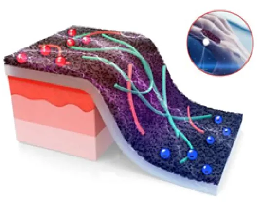
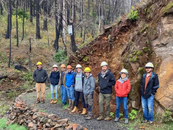
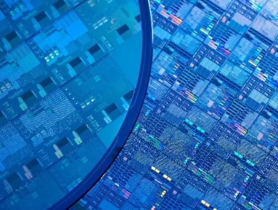
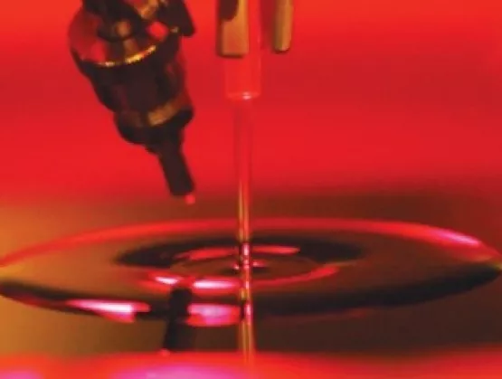
In a world where technological advancements move at lightning speed, the semiconductor industry is facing unprecedented challenges. The demand for smaller, faster, and more energy-efficient devices is growing, and traditional manufacturing processes are being pushed to their limits. Enter Spin-on Dielectrics (SOD), a breakthrough material technology that offers a cost-effective, scalable solution for micro-gap filling and high-performance dielectric films. As the industry evolves, SOD is expected to play a pivotal role in enabling the next generation of chips that power everything from AI to everyday electronics.To learn more, SEMI Europe and Merck KGaA, Darmstadt, Germany, held a joint webinar that focused on semiconductor device process evolution by SOD. The session featured insights from three technology experts in the company, including Dr. Surésh Rajaraman, Executive Vice President and Head of Thin Film Business Unit, along with Atsuko Yamamoto, R D Manager for Spin-On Dielectric, and Go Nakano, Global Marketing Manager for Dielectric Materials.SEMI: What is SOD, and how does it fit within the broader semiconductor manufacturing process?Rajaraman: SOD, Spin on Dielectrics, is a unique class of materials used to deposit thin layers of dielectric films, which act as insulators or other functional films, on semiconductor devices. The fabrication of a semiconductor chip involves thousands of intricate steps that incorporate conductors, semiconductors, and insulators. SOD is a versatile technology that supports device performance and miniaturization by enabling better gap fill and film uniformity, all while offering attractive cost of ownership.SEMI: Why is there so much focus on SOD materials, and how are they evolving to meet future industry demands?Rajaraman: As semiconductor devices become more complex—such as 3D NAND scaling to more than 300 layers and DRAM incorporating pillar capacitors—there’s a growing need for materials that can address challenges like interconnect delays, power consumption, and heat generation while maintaining optimal performance. Traditional dielectric materials are reaching their limits, making Spin-on Dielectrics (SOD) a critical solution. SOD offers advantages like bottom-up and seam-free gap filling, enabling ultra-thin insulating and other functional layers that enhance electrical and thermal efficiency and support next-generation device scaling.The industry is pushing the boundaries of scaling, with increasing aspect ratios and complex structures in Logic, 3D NAND and DRAM. Modern devices now require deposition in features which are not only incredibly narrow but also increasingly deep due to going into the third dimension. This creates new challenges, such as stress buildup and cracking in conventional SOD materials. To overcome this, we are developing enhanced formulations with improved mechanical stability and polymer backbone engineering. These innovations enhance gap-filling properties and resistance to process-induced stress, ensuring SOD remains a key enabler for advanced semiconductor manufacturing.SEMI: What are the current industry trends driving the adoption of SOD?Nakano: SOD is becoming a key technology because of its excellent gap-filling performance. Unlike gas-phase deposition methods like Chemical Vapor Deposition (CVD) and Atomic Layer Deposition (ALD), SOD is a liquid-phase process. This makes it more efficient for high-aspect-ratio structures. It also helps reduce costs while maintaining high-performance dielectric properties.With increasing demand for high-density memory and logic devices, SOD is crucial for applications like DRAM and NAND flash, which require precise dielectric layer formation. In DRAM, we’re witnessing a shift from planar to vertical transistors, and even to monolithic 3D DRAM. These changes require new materials for gate insulators and electrodes, alongside improvements in aspect ratio gap filling.For NAND memory, manufacturers are increasing the number of memory layers, leading to taller memory stacks and deeper trenches. As lateral scaling progresses, narrower and more complex structures demand high-aspect-ratio trench fills to maintain performance and reliability.Logic devices are also evolving, with transistor structures moving from FinFETs to nanosheets and forksheets. This transition enhances performance, but it also introduces challenges in wiring density and electrical properties. The narrower pitch of wiring requires advanced dielectric solutions, like SOD, to enable reliable, high-performance semiconductor architectures.SEMI: With all these recent innovations, what role does Merck KGaA, Darmstadt, Germany play in supporting these advancements, and what does the company offer its customers? Rajaraman: As the semiconductor industry pushes the boundaries of scaling, doing so requires materials that can support increasingly complex structures. We are the only materials company in the industry to possess the full spectrum of process technologies for gap-filling capabilities, including SOD, ALD, CVD, and Flowable CVD. Our strategic acquisition of Versum Materials has expanded our capabilities with organosilicon precursors. Combined with our SOD expertise, it allows us to reengineer material backbones with more material choices and tailored properties to optimize performance in high-aspect-ratio applications.To support this, we’ve expanded our global R D footprint. We now operate in various application labs, enabling close collaboration with customers for material customization and fine-tuning properties to address specific manufacturing challenges. Last year, we inaugurated a new R D center in Korea as part of our commitment to being near our customers and accelerating time-to-market for next-generation semiconductor solutions. As semiconductor roadmaps become more complex, customization and collaboration also become more critical. The key to innovation lies in working closely with our customers, understanding their challenges, refining materials, and optimizing processes together. By fostering this ongoing partnership, we can accelerate technological advancements and ensure that new solutions align seamlessly with evolving industry demands.SEMI: Can you share some technical insights on SOD?Yamamoto: SOD is a key material used in semiconductor manufacturing to create insulating layers with high precision. One of the essential components in SOD is PHPS (Perhydropolysilazane), a polymer composed of silicon, nitrogen, and hydrogen. This material is applied as a liquid solution and transforms into a high-quality silicon oxide film through a series of thermal processes.PHPS is essential because it enables precise gap filling in extremely small structures, helping to improve device reliability. The process involves spin-coating the polymer onto a wafer, followed by pre-baking to remove solvents. Then, it undergoes high temperature curing in an oxygen and steam atmosphere, forming a dense silicon oxide film. This method ensures uniform coverage and cost efficiency compared to traditional dry film deposition techniques.Our Spinfil® product line has evolved over the past two decades, starting with the Spinfil® 400 series and advancing through the Spinfil® 600 to the widely used Spinfil® 800 series. These improvements have enhanced gap-filling capabilities and film uniformity, making them ideal for high-aspect-ratio trench structures. The critical baking process involves spin coating and pre-baking before wafers undergo batch processing in a high-temperature furnace. Controlled temperature and moisture conditions transform Spinfil® into silicon oxide films, optimizing properties such as refractive index, shrinkage, and etching resistance and ensuring reliability in semiconductor applications.SEMI: What are the latest trends in new polymer development for SOD?Yamamoto: Our research focuses on three key areas: enhancing film quality, developing SOD for high-aspect-ratio trench filling, and advancing low-k SOD for semiconductor processes.To improve film quality, we introduced the Neofil®series, an evolution of the Spinfil® 800 series. This innovation reduces film shrinkage, lowers stress, and enhances wet etching rates, making it ideal for next-generation semiconductor nodes.Our latest Neofil® series for high-aspect-ratio trench filling is targeted for traditional dry processes like CVD and ALD, which can often lead to void formation and require multiple deposition-etch steps. Our latest SOD materials address this by improving polymer elasticity, ensuring uniform filling of deep trenches up to 16 microns without cracks, making them suitable for emerging 3D nanostaircase designs.In low-k SOD development, we’re focusing on siloxane-based polymers, which provide excellent trench-filling capabilities while maintaining strong mechanical and electrical properties. Compared to flowable CVD and ALD, SOD offers a more cost-effective and efficient alternative. With continued advancements, we anticipate SOD will become a key material for future semi-damascene processes, enhancing embedding performance and overall device reliability.SEMI ContactSitong He, Communications Manager Email: [email protected]
Read More
As the global semiconductor industry charges toward a projected $1 trillion market by 2030, regional innovation hubs are stepping into the spotlight. The inaugural SEMIEXPO Heartland—held April 1–2, 2025, at the Indiana Convention Center in Indianapolis—brought together key players from across the ecosystem to explore how advanced packaging, smart manufacturing, smart mobility, AI, and workforce development are fueling the semiconductor revolution.With a special focus on building self-reliance in the U.S. chip supply chain, the event highlighted efforts that are revitalizing the Midwest’s role as a key region driving innovation in the global semiconductor ecosystem. SEMIEXPO Heartland showcased leading-edge strategies and technologies from global giants and regional champions alike—underscoring the deep connections between government, academic, research, and industry leaders.Keynote HighlightsSK hynix: Accelerating the Future with Chiplets and Advanced PackagingDr. Woong Sun Lee, Senior Vice President at SK hynix, kicked off the event with a powerful vision for the future of semiconductor manufacturing. In response to skyrocketing demand fueled by AI, autonomous vehicles, and next-gen mobile applications, SK hynix is pursuing aggressive innovation through heterogeneous integration and chiplet-based design.Using 12-inch wafers, SK hynix’s chiplet strategy compresses product development timelines from 10-20 years to as little as 2-5 years. This leap in design efficiency enables faster time-to-market and greater performance optimization—crucial in an industry where speed and scale are paramount.A major component of this vision is the company’s investment in a state-of-the-art advanced packaging facility in Indiana. Targeting mass production by 2028, the new hub will not only expand SK hynix’s U.S. manufacturing footprint but also support national goals around workforce development and ecosystem growth. It’s a bold move that aligns the company’s R D leadership with America’s strategic reshoring efforts.Robert Bosch Semiconductor: Driving the Future with Silicon Carbide (SiC)Thorsten Scheer, Regional President Mobility Electronics and Plant Manager at Bosch Roseville, presented a deep dive into how Bosch is preparing for the electrified mobility era. Central to Bosch’s strategy is the adoption of silicon carbide (SiC) semiconductors, which are increasingly critical to electric vehicle powertrains.As vehicles become more connected and automated, Bosch projects more than 40 semiconductor chips per car by 2035. To meet this demand, Bosch is developing dual-channel trench MOSFET technology using SiC—a move that enhances power conversion efficiency and reduces heat, two of the biggest challenges in EV design.Bosch’s global expansion includes a new SiC wafer fab in Roseville, California, which is set to begin production in 2026. This facility is not only a technological investment but also a commitment to supply chain resilience, ensuring that the U.S. plays a central role in future automotive innovation.Polar Semiconductor: Reshoring Advanced Foundry CapabilitiesSurya Iyer, President and COO of Polar Semiconductor, shared the company’s mission to reinvigorate America’s semiconductor manufacturing capabilities. Headquartered in the Midwest, Polar is a rare U.S.-owned foundry playing a strategic role in reshoring production and building domestic capacity.Specializing in power semiconductors—including MOSFETs, IGBTs, and wide-bandgap (GaN) devices—Polar focuses on serving critical sectors such as automotive, aerospace and defense, and industrial applications. With advanced automation and a commitment to cost-efficient scale, the company is helping to bring more semiconductor innovation back to U.S. soil.Polar’s flexible business models and emphasis on workforce training position it as a linchpin in the nation’s efforts to build a more secure and agile semiconductor supply chain.Smart Manufacturing and Mobility SessionsUnlocking the Future with AI, Edge, and Digital TwinsThe opening session on April 1 showcased how AI and advanced simulation are transforming the semiconductor manufacturing process. NHanced Semiconductor introduced "Foundry 2.0," a platform delivering chiplet-based solutions tailored for low-volume, high-mix applications—highlighting flexibility and speed.Kulicke Soffa emphasized the use of AI, digital twins, and agentic automation in backend operations, helping to cut costs and boost efficiency. Humatics demonstrated its Milo microlocation system, addressing factory automation and labor challenges with precision positioning technologies.Meanwhile, Purdue University’s research in chip-package co-design and semiconductor education reflected the essential role of academia in building future-ready capabilities.AI, Edge, and Digital Twins in Backend ManufacturingThis session continued to explore the shift toward intelligent, connected manufacturing ecosystems. Allan Lewis of Nordson Electronics Solutions showcased AI-powered inspection systems that reduce downtime and improve yield.Jim Redman from ErgoTech Systems emphasized the importance of scalable, decentralized data platforms using low-code tools. Luis Rivera of Koh Young Technology introduced KSMART Server and CFX standards, enabling real-time optimization and machine-to-machine communication.Josh Mangahas from INFICON detailed how digital twins and AI/ML models are enhancing production scheduling and delivery timelines, while Mahesh Deshpande of Dassault Systèmes illustrated how virtual twins and XR-based tools are supporting agile packaging environments.The Convergence of AI, Robotics, and Digital TwinsSession 3 on April 2 featured cross-disciplinary insights from leaders at Arizona State University (ASU), Fraunhofer IZM, Teradyne, and Purdue. A common theme: AI, robotics, and digital twins are converging to redefine factory dynamics.Dr. Binil Starly (ASU) explained how reinforcement learning and MQTT protocols are enabling adaptive robotic inspections. Erik Jung (Fraunhofer IZM) highlighted how packaging and AI systems evolve in tandem to achieve tighter integration and higher performance.Teradyne’s Mat Najibnia focused on the ROI of robotic material handling systems, while Purdue’s Dr. Martin Jun shared a vision for democratized smart manufacturing—especially for small and medium-sized manufacturers (SMMs).Building Future-Ready Semiconductor EcosystemsThe final session underscored the importance of collaboration, resilience, and cybersecurity. Athinia discussed its work harmonizing raw material and fab data to improve manufacturing insights. IBM presented use cases combining digital twins and generative AI for yield improvement and predictive maintenance.Siemens focused on sustainability and decarbonization through digital twin platforms. The Florida Semiconductor Engine (FSE) illustrated how regional ecosystems can support leadership in packaging innovation and talent development.PEER Group spotlighted the Semiconductor Manufacturing Cybersecurity Consortium (SMCC), advocating for a standardized, collaborative approach to securing manufacturing infrastructure.Workforce Development and Regional ImpactA strong undercurrent throughout SEMIEXPO Heartland was the need for strategic workforce development. The event featured a Workforce Pavilion offering job seekers access to career coaching, resume guidance, and mentorship.Local universities and community colleges were well represented, as were federal and state workforce programs. These partnerships are crucial to ensuring a robust talent pipeline and equipping workers with the skills needed for a rapidly evolving industry.The presence of SK hynix, Polar, and other major players making sizable investments in the Midwest signaled not just a resurgence of regional manufacturing, but a renewed commitment to community growth, equitable opportunity, and long-term sustainability.A Midwest Moment with Global ImplicationsSEMIEXPO Heartland 2025 captured a pivotal moment in the evolution of the semiconductor industry. From chiplets and SiC to AI-driven smart factories and cyber-resilient ecosystems, the event highlighted how innovation, collaboration, and policy alignment are driving progress.As America looks to fortify its semiconductor future, the Midwest is emerging as a powerhouse of talent, technology, and tenacity. With support from industry, government, and academia, the region is well-positioned to lead the charge into a smarter, more secure, and more resilient semiconductor era.For questions about SEMI’s Smart Manufacturing initiative, contact Anshu Bahadur at [email protected]. Read more about SEMIEXPO Heartland in this press release: Inaugural SEMIEXPO Heartland Event Underscores Midwestern U.S. as a Global Hub for Smart Manufacturing and Smart Mobility.Anshu Bahadur is Sr. Program Manager, Technology Communities at SEMIRafael Tudela is Sr. Technical Marketing Manager at SEMI
Read More