downloadGroupGroupnoun_press release_995423_000000 copyGroupnoun_Feed_96767_000000Group 19noun_pictures_1817522_000000Member company iconResource item iconStore item iconGroup 19Group 19noun_Photo_2085192_000000 Copynoun_presentation_2096081_000000Group 19Group Copy 7noun_webinar_692730_000000Path
Skip to main content
Several years ago, the ESD Alliance, a SEMI Technology Coalition contacted Jay Vleeschhouwer, Managing Director of Software Research at Griffin Securities, about his yearly presentation on the state of EDA and the industry’s successes during the Design Automation Conference (DAC). He willingly agreed, and it has been a yearly tradition for our executives to interview Vleeschhouwer.This year is no exception. He took time to chat with us about this year’s presentation and his findings that show EDA’s phenomenal revenue growth and startup activity. Our talk covered EDA mergers and acquisitions, AI and what’s next.In his presentation, Vleeschhouwer references the ESD Alliance quarterly Electronic Design Market Data (EDMD) report on EDA, Semiconductor IP and Services industry revenue data from public and private companies. Rogers: EDA has grown continuously since 2010. What do you attribute the growth to? The revenue numbers suggest it's sustainable.Vleeschhouwer: The growth can be attributed to many of the factors that have been in place for many years now. What we have observed from the ESDA (EDMD) market data, for example, is that numerous categories, which we include in our quarterly report, have been growing continuously on a trailing 12-month basis for many years. There are far more categories that are growing than are not growing. In fact, very few categories show no growth or little growth.The growth has been diverse across the categories, a crucial underpinning for growth in the industry. It is also different from the situation a quarter century ago or more. I often make this point to investors when speaking about EDA. Years ago, the growth would typically be much more limited in terms of the product categories that perhaps one or two categories would be showing good growth or well above industry average growth. Those would eventually run their course.Now, what we've seen is multiple categories growing, in some cases, well above the industry average. That is driven by technology needs on the part of the customers. In other words, when you think about how the whole design and engineering process has evolved, requiring more product categories to be integrated, to be used heuristically, then that underpins the improved and more diverse growth across the industry that we've seen now for many years.It also ties into what’s gone on with the two largest vendors, Cadence and Synopsys. This ties directly to why their market share has gone from just over half of industry revenue now to nearly three-quarters of industry revenue. Their portfolios have become increasingly diverse and more integrated. A lot of that was inorganic through acquisition, but mostly in the last number of years through internal development. These growth phenomena and market share phenomena are highly correlated.Rogers: How is AI impacting industry growth in the EDA companies themselves? Should we expect a flurry of mergers and acquisitions?Vleeschhouwer: The first of those two questions is an important one. Unfortunately, we don't have a great answer yet. We've been encouraging the largest vendors to be more explicit to the extent they can be about the AI impact on their business. Cadence and Synopsys have separately branded AI products or agents. Cadence has a family of products. Synopsys has its family of products. Those are separately priced.We would love to see over time how those are contributing to revenue. At the same time, or over time, we do expect not only EDA, but for all our Engineering Software companies, AI will become increasingly infused in legacy products. It's just going to become part of the capabilities naturally offered to customers. We’re going to see hybrid portfolios that we have today separately branded as additional flavors, and those capabilities will be increasingly embedded as well.As that occurs, it would naturally become more difficult to separately attribute revenues to AI, but to the extent that there are separate brands, then it should be possible for the companies to be more explicit about those contributions. Synopsys will be hosting an investor day in New York at the end of September. I'm sure this question will come up as to the contribution of AI, among many other questions. At this point, all I can say is our observation is that, of the three major categories that we define as Engineering Software—EDA, Technical Software, and architecture, engineering, and construction (AEC)—it appears AI availability, customer adoption and production is further along in EDA.That observation is based on customers’ commentary and presentations at, for example, the Cadence conference and the Synopsys conference. It's that accumulated customer presentation and availability of customer results that suggests that AI adoption is further along in that part of Engineering Software, and the rest will undoubtedly follow over time. On the Technical Software side or industrial side of Engineering Software, the AEC side, I have no doubt it will become increasingly important. So far, however, for some good technical reasons, we think AI adoption is further along in EDA.Cohen: You mention the EDMD report on industry revenue in your DAC presentation. The numbers reported are not the same as the numbers you tend to report in your publications. Can you discuss the differences?Vleeschhouwer: Yes, thank you for the easy question. I was waiting for that one. As you know, we've been using this data for over a quarter of a century, every quarter. I always make the distinction in the report that the difference between what the SEMI/ESD Alliance report shows and what my report shows is a single category, and that is non-reporting-company IP.We include reporting-company IP, but for the purpose of our parsing of the data, we exclude from the total and from the growth comparisons what the market data refers to as the non-reporting-company IP. In all other respects, the categories line up. As much as possible, we try to correlate the industry data by geo and by category to the company results for market share calculation purposes, for growth purposes, and the like. Rogers: What should SEMI readers be looking for in terms of 2027 EDA revenue?Vleeschhouwer: All I can do is repeat what we've published in our industry report, which is that we expect industry growth to exceed $17 billion this year. That's based on our estimates for Cadence's revenues, what we call Synopsys Classic, plus an assumption for the EDA part of Ansys, and only the EDA part of Ansys, plus some assumption for Siemens EDA. Siemens EDA has done well since Mentor was acquired over nine years ago. That business has doubled since Mentor's last year as a public company. That includes some small acquisitions that Siemens has since done, but again, the overall business has roughly doubled.The business, I should also point out, on a quarterly and even annual basis, can be quite variable at Siemens because of the nature of their revenue models. Taking that into account, again, we expect over $17 billion this year in industry revenue, as compared with nearly $16 billion in 2025. This should be another good year for EDA. With respect to 2027, we haven't yet published an industry forecast. I have no doubt it will continue to grow, but we have only published forecasts for Cadence and Synopsys individually. Even though they still account for almost three-fourths of the industry, we would have to give a number for the other, more than one-fourth of the industry, which at this point we've not yet published.About Jay Vleeschhouwer  Jay Vleeschhouwer, Managing Director of Software Research at Griffin Securities, has more than 40 years of research analyst experience in the technology sector, including software, semiconductors and computer hardware. Julie Rogers is executive director of the ESD Alliance.  Paul Cohen is Senior Manager of the ESD Alliance.
Read More
The counterfeit semiconductor market is estimated to be multi‑billion‑dollar in scale. OBSIDIA's own customer interviews put the true toll above $100 billion a year, touching everything from foundries losing 5%+ of revenue to counterfeits to failures downstream that cost reputation, business, or lives.As semiconductor devices become increasingly central to artificial intelligence, critical infrastructure, automotive systems, and national security applications, trust in the underlying hardware is emerging as a strategic concern. While the industry has made significant progress in tracking materials, documenting supply chains, and improving cybersecurity, questions remain around authenticity, provenance, and whether organizations can truly trust the devices powering modern technology.To explore these challenges, SEMI’s Mayura Padmanabhan and Nishita Rao spoke with Erik Hosler, Founder and CEO of OBSIDIA Semiconductors Inc, about counterfeit electronics, traceability, trusted hardware, AI infrastructure, and the role industry collaboration can play in securing the semiconductor ecosystem.For readers who may not be familiar with OBSIDIA, what challenge is the company trying to solve?Hosler describes OBSIDIA's mission through a comparison that many technology professionals immediately understand."OBSIDIA is focused on delivering security at the hardware level for the semiconductor industry. A great way to think about that is the analog of antivirus in software." While software has long benefited from tools that help validate and protect systems, he believes the semiconductor industry has lacked an equivalent capability at scale for hardware."Nothing really exists in the semiconductor ecosystem on a large scale for hardware security. The ability to really trust that the semiconductor devices that we rely on every day are authentic and conforming." That gap is what OBSIDIA aims to address. By examining the physical characteristics of devices, the company seeks to verify authenticity at multiple points throughout the semiconductor lifecycle."Through our technology, we're able to authenticate the integrity and quality of devices at any level of integration within the semiconductor supply chain, from the wafer level all the way up to and including the application." This capability was demonstrated as part of a DARPA Small Business Innovation Research (SBIR) Phase II award OBSIDIA completed a few years ago as well as projects with MITRE and Kostas Research Institute for Homeland Security.Why has semiconductor authenticity become such an important issue today?According to Hosler, semiconductor authenticity is no longer a niche concern. As the world becomes increasingly dependent on electronics, the potential impact of counterfeit and non-conforming devices continues to grow."There have been a lot of studies over the past couple of years analyzing how many of these types of devices are actually in our ecosystem. Even at the highest level of scrutiny within the Department of Defense in the U.S., anywhere from 10 to 15 percent of their electronics contain counterfeit devices. That's a very scary statistic."The issue extends beyond critical systems and into everyday life."The chance that you have a counterfeit device in one of your electronics within arm's reach at any point in time during the day is very real." Interestingly, Hosler does not characterize counterfeiting primarily as sophisticated malicious activity."It's not a targeted event. It's a crime of opportunity." He pointed to supply chain disruptions as examples of how legitimate shortages can create openings for non-conforming devices to enter the market."Counterfeits aren't just something bought off the back of a truck. They're sprinkled into our ecosystem and appear seemingly at random." SEMI's Traceability Phase Zero discussions highlighted industry concerns around provenance, authenticity, lifecycle visibility, and supply chain assurance. From your perspective, what are the biggest traceability challenges facing the semiconductor industry today?When discussing traceability, Hosler pointed to a challenge that extends beyond tracking high-value chips themselves."Let's say we have a $30,000 NVIDIA GPU. Tracking that through the supply chain is dollar-for-dollar kind of equivalent to tracking a car through the supply chain. You're going to want to make sure you know where that asset is at any point in time."The challenge begins after that component becomes part of a larger system."Where this paradigm breaks is at integration." Modern electronics consist of hundreds of interconnected components. Even when a high-performance processor has been carefully tracked and validated, a much smaller supporting component can introduce unexpected risk."If one of those five-cent devices on that PCB is counterfeit, it compromises the entire performance of that board, and by extension, that $30,000 GPU." That observation became one of the defining themes of our conversation:“A $30,000 GPU can be compromised by a five-cent component.” For Hosler, true traceability cannot stop at flagship devices. It must extend across entire assemblies and systems.OBSIDIA was recently named among the seven companies signing U.S. CHIPS and Science Act letters of intent for compute supply chain R D. What does this recognition say about the growing importance of hardware trust and security within the semiconductor ecosystem?Hosler views the recognition as evidence that the industry is paying increasing attention to the importance of trusted hardware."What the CHIPS R D money allows us to do is accelerate the commercialization of the technology."He noted that OBSIDIA has already moved beyond the lab and into commercial deployment."We already have a system deployed at a commercial site today. We are in the field running our machine, collecting data with our customer, providing feedback to their customers and suppliers about what's happening in the ecosystem." The funding, he explained, helps accelerate the journey from research to industry adoption while enabling the company to scale its technology across a growing number of use cases.Hosler also contrasted OBSIDIA's approach with current industry practices."If you receive a thousand devices, you typically send three of those devices out for validation at a third-party lab. Then you have to assume the other 997 were authentic."OBSIDIA's vision is to move beyond sampling."What OBSIDIA allows you to do is measure every single device that you receive." By reducing dependence on sample-based validation, organizations gain the opportunity to improve confidence in every component entering their manufacturing process. Many companies already have authentication, tracking, or security technologies. What is still missing to achieve true end-to-end traceability across the semiconductor lifecycle?A recurring theme during industry traceability discussions is the tension between sharing information and protecting intellectual property.Hosler acknowledged that companies are understandably protective of their manufacturing knowledge, process data, and design information."There is a strong desire to control IP, control process data, and control yield data." Rather than attempting to change that reality, OBSIDIA designed its technology around it."So OBSIDIA really looked at its technology and asked how we can be IP and data agnostic." That philosophy led to one of the most memorable statements from the interview:“We're the company that knows nothing.”Hosler explained that customers can maintain existing workflows, processes, and controls without exposing sensitive data."You can maintain whatever structures and regulations and procedures you have already and we will be an addition to that without any need to know anything about what you are doing."By focusing on spectroscopic measurements rather than imaging or design extraction, the company seeks to strengthen trust without requiring access to proprietary information. As AI systems become increasingly important in commercial and national security applications, how does trust in the underlying hardware affect trust in AI itself?Artificial intelligence emerged repeatedly throughout the discussion, particularly as organizations invest heavily in AI infrastructure and advanced computing systems."The AI infrastructure buildout is one of the greatest projects within the U.S. from a manufacturing perspective that has happened in decades." Hosler sees this expansion as both an opportunity and a responsibility for the semiconductor industry."AI is going to be active in the systems that we directly engage with on a daily basis, whether that's the plane you're flying on, or the car you're driving." As AI becomes integrated into transportation, industrial automation, critical infrastructure, and consumer applications, trust in the underlying hardware becomes increasingly important.Drawing a comparison to the evolution of cybersecurity, Hosler believes the industry is approaching an important moment."We don't want to end up with a major incident that we all look back on as a major misstep by us in the industry, just like we saw with cybersecurity." "We are poised for a similar incident when it comes to hardware security." Where do you see the greatest opportunities for progress in the next three years, and how can SEMI help support that progress?Despite the challenges, Hosler remains optimistic about the industry's direction."I think where we are seeing the most progress is the recognition of the problem." He pointed to increasing attention from government, industry, and technology providers as evidence that momentum is building around hardware trust and infrastructure assurance."This is a major opportunity for the industry to rally around that call and deliver a solution that not only covers AI space but covers the rest of our infrastructure as well." Hosler also sees a critical role for standards organizations."SEMI is the perfect place, given that all the partners are already there, all the end customers, all the interested parties." Reflecting on SEMI's Traceability Phase Zero effort, he described it as an important starting point that helped identify both challenges and opportunities."The Phase Zero study was a great first step to realize what the challenges are and what the potential opportunities are. Now a Phase One is required to consolidate the feedback and align on a solution." One trend worth watching going forward: the industry's accelerating shift toward chiplets and multi-vendor advanced packaging means a single finished package can now contain die from several different suppliers, assembled by a third party - a structural change to the supply chain that raises new provenance questions of its own.Closing ThoughtsAt the conclusion of our discussion, Hosler offered a simple piece of advice for organizations focused on quality, trust, and supply chain security:“Be skeptical.” He encouraged leaders to look beyond documentation and assumptions and spend more time understanding what is happening on the factory floor."Even though everything looks okay on the outside, what's happening on the factory floor could be a very different story.""Don't assume everything is okay. Dig that next layer deeper." As semiconductor supply chains become increasingly complex and AI systems become more deeply embedded in everyday life, trust can no longer be viewed solely as a matter of paperwork, compliance, or process. As Hosler emphasized throughout our conversation, building confidence in modern technology ultimately begins with confidence in the hardware itself. About Erik HoslerErik Hosler is Founder of OBSIDIA Semiconductors, a company focused on semiconductor authenticity, hardware trust, and supply chain security through advanced RF-based device verification technologies. OBSIDIA's mission is to enable scalable, non-destructive verification of semiconductor devices across the electronics lifecycle Mayura Padmanabhan is a Technical Project Manager at SEMI, focused on advancing semiconductor cybersecurity, traceability, and supply chain resilience through industry standards and collaborative initiatives. Nishita Rao is Director of Product Marketing at SEMI, leading global marketing initiatives that drive industry engagement, thought leadership, and awareness across the semiconductor value chain.
Read More
Taiwan is entering a decisive decade. The rapid growth of artificial intelligence, advanced semiconductor manufacturing, and high-tech information and communications technology (ICT) supply chains is increasing the strategic importance of electricity availability, cost stability, and progress toward net-zero by 2050. For Taiwan’s semiconductor and high-tech industries, energy is no longer only an operational matter. It is increasingly connected to competitiveness, supply chain resilience, customer expectations, and long-term investment confidence.Within this broader transition, renewable energy remains one of the most important tools available to corporate off-takers. Larger-scale renewable energy resources, including offshore wind, can play a strategic role in supporting post-2030 electricity demand and strengthening Taiwan’s position as a trusted global technology hub. However, the central challenge is no longer simply whether renewable energy demand exists. The more urgent question is how that demand can be converted into bankable, executable, and scalable procurement pathways.Against this backdrop, SEMI Energy Collaborative (SEMI EC) explored the Group Buy Initiative not as a single procurement model, but as a broader study of collaborative pathways that could strengthen Taiwan’s high-tech sector as it moves from renewable energy demand signals toward practical market delivery. The study identifies three possible directions: a straightforward Group Buy Program, Qualified Anchor Investment, and a JV-Aggregator model that could serve as a scalable bridge between renewable energy developers and a broader base of corporate off-takers.Renewable Energy as an Industrial Competitiveness IssueFor many companies, renewable energy procurement has historically been discussed through the lens of sustainability reporting, supply chain requirements, or corporate commitments. Those drivers remain important, but the context has changed. In the AI era, renewable energy procurement is becoming a strategic enabler of broader industrial strategy. This shift creates a practical market question: can disclosed corporate demand be converted into bankable long-term contracts and workable procurement mechanisms? The answer depends on whether developers, corporate off-takers, financial institutions, and government agencies can align around transaction structures that are commercially workable, financeable, and aligned with Taiwan’s evolving electricity-market rules.SEMI EC’s role in this context is to support market understanding, structured dialogue, and voluntary collaboration. The Group Buy Initiative study was therefore designed to examine possible collaborative pathways and identify scalable market solutions, not to prescribe a single procurement direction.Clear Demand Signals, Slow Market ConversionMany large and medium-sized companies have already disclosed renewable energy requirements, decarbonization milestones, supply chain expectations, or corporate commitments through annual reports, sustainability reports, ESG disclosures, and public statements. These signals indicate that substantial corporate demand exists and that renewable energy procurement is becoming increasingly critical to long-term business planning.The more important question is why these demand signals have not translated more quickly into actual market deployment. Demand disclosure alone does not automatically create bankable projects or executable Corporate Power Purchase Agreements (CPPAs); it must be translated into transaction-ready structures with sufficient offtake certainty, risk allocation, credit support, certificate clarity, and regulatory certainty.In other words, Taiwan’s challenge is not only a renewable energy demand challenge. It is a market-conversion challenge. The task is to build the structures, mechanisms, and confidence needed to convert disclosed demand into bankable and executable renewable energy procurement pathways. This is where collaborative models may have a role. The Group Buy Initiative study therefore shifted its focus from demand assessment to pathway assessment, asking which collaborative structures could most effectively bridge the gap between renewable energy demand signals and executable market transactions. The CPPA Challenge: Availability, Accessibility, Affordability, and AcceptabilityThe market-conversion challenge is especially visible in CPPAs. In Taiwan, offshore wind CPPAs are particularly complex because they must satisfy several requirements at once: project bankability, buyer readiness, regulatory compliance, certificate treatment, and internal approval.The Group Buy Initiative study categorizes CPPA execution barriers across four dimensions: availability, accessibility, affordability, and acceptability.Availability refers to whether sufficient renewable energy projects can be delivered on time and at scale. Taiwan has made important progress in renewable energy development, but larger-scale projects continue to face execution pressures, including cost escalation, financing uncertainty, supply chain constraints, permitting complexity, and policy-design challenges.Accessibility refers to whether corporate buyers can access renewable energy through workable procurement structures. Large-scale offshore wind projects often require highly bankable off-takers to support project financing. As a result, not every company with renewable energy demand can easily sign a direct project-level CPPA. Some buyers may still be building the credit readiness, balance sheet capacity, internal procurement process, or long-term risk-management experience required for this type of transaction.Affordability refers to the price gap between renewable energy CPPAs and regulated electricity tariffs or other available procurement options. For many companies, especially those under cost pressure, it is difficult to justify long-term renewable energy procurement unless the price, risk allocation, and certificate treatment are sufficiently clear.Acceptability refers to whether CPPA terms can pass internal review. A CPPA is not a simple “sign-and-forget” transaction. Companies must evaluate whether project delivery, contract tenor, generation profile, Surplus RE exposure, Taiwan Renewable Energy Certificate (T-REC) allocation, settlement and accounting treatment, and approval requirements can be managed within their internal governance framework. These issues are manageable, but they require greater market understanding and more structured engagement.Figure 1: Major Challenges for Offshore Wind CPPA in TaiwanOffshore Wind: A Strategic Pillar Under Execution PressureTaiwan’s offshore wind sector is facing real execution pressure. These challenges should not be understated, but they should also be understood as part of the market’s ongoing transition rather than as a reason to step back from larger-scale renewable energy development. Offshore wind remains strategically relevant because of its scale, generation profile, and potential contribution to post-2030 industrial electricity demand.For Taiwan’s semiconductor and high-tech ICT sectors, offshore wind is therefore not only a source of renewable electricity. It is a strategic component of Taiwan’s long-term industrial competitiveness. However, the same characteristics that make offshore wind strategically important also raise the execution threshold: projects must secure lender-grade revenue certainty while giving corporate buyers workable solutions for credit, settlement, T-REC allocation, and Surplus RE exposure.This led to a key conclusion from the Group Buy Initiative study: the most intuitive collaborative model is not necessarily the most executable. A straightforward Group Buy Program can support coordination and readiness, but offshore wind procurement also requires a transaction structure capable of meeting lender, developer, and corporate-buyer requirements at scale. This is why aggregator-based and investment-linked pathways deserve further assessment alongside more conventional procurement models.Rethinking Collective Action: From Obvious Options to Practical PathwaysThe Group Buy Initiative study examined collective action from a practical market perspective. Rather than assuming that one model could solve all procurement barriers, the study considered three possible pathways. Each pathway addresses a different part of the market-conversion challenge.One of the clearest observations is that the most obvious option is not always the easiest to implement. A Group Buy Program appears straightforward at first: companies with renewable energy demand could aggregate interest, align common procurement principles, and engage developers through a more coordinated process. In theory, this could reduce transaction costs, improve transparency, and convert disclosed demand into a more actionable procurement signal.In practice, however, Taiwan’s market conditions make a straightforward Group Buy Program more complicated. Larger and more creditworthy off-takers may already be able to negotiate directly with renewable energy developers, while smaller or medium-sized off-takers may benefit more from collective procurement but may not individually provide the bankability that project-financed offshore wind projects require. This creates an anchor gap: the companies most able to support project finance may have less need for a Group Buy structure, while the companies most likely to benefit from Group Buy may not be sufficient to support project finance on their own.This does not mean that a Group Buy Program has no value. It can still serve as a useful platform for demand mapping, member segmentation, CPPA capacity building, common-term discussion, and market signaling. However, the study suggests that the Group Buy Program should be understood primarily as a coordination and readiness-building pathway, rather than a simple shortcut to large-scale offshore wind procurement. Any structure that involves shared procurement, aggregated demand, or anchor participation would still require careful legal, financial, credit, and competition-law review.This is where the JV-Aggregator pathway becomes relevant as a potential market-enabling structure. Taiwan already has 125 registered renewable energy sellers, according to publicly available Energy Administration information as of 1 July 2026. However, many appear to be focused on solar PV or smaller-scale transactions and may not have the scale, credit profile, balance sheet capacity, or client base required to engage with offshore wind developers. This creates an imbalance: offshore wind developers need credible and scalable offtake partners, while many existing aggregators may not yet be able to serve that role.Under current market conditions, a larger and more institutionally credible JV-Aggregator could address several gaps that a straightforward Group Buy Program may not fully resolve. Such a platform could potentially be developed through partnership, strategic investment, or by leveraging existing licensed market capabilities, followed by credit enhancement, governance strengthening, and clearer market positioning. If properly structured, it could provide a more scalable interface between larger renewable energy developers and a sector-focused corporate off-taker base.For developers, an aggregator-based model could provide a more credible route to diversified corporate demand. For off-takers, it could offer more flexible procurement arrangements than direct project-level CPPAs, particularly for companies that have renewable energy demand but may not be ready or able to serve as standalone bankable anchors. In this sense, the JV-Aggregator pathway appears to address practical market gaps related to scale, credit intermediation, customer aggregation, settlement, and allocation.However, this pathway would require careful qualification. A JV-Aggregator would need to demonstrate institutional capacity across capitalization, credit support, retail licensing, pricing transparency, T-REC accounting, settlement and allocation, risk management, and governance. If connected to an industry platform in any form, it would also require safeguards to preserve member independence, avoid competition-law concerns, and ensure that any associated industry platform remains a neutral facilitator rather than a commercial contracting party.Qualified Anchor Investment remains a third and more selective pathway, and may include SPV-type participation in selected renewable energy projects or platforms. For companies with sufficient capital capacity, investment mandate, and long-term renewable energy demand, strategic capital participation may help improve project bankability and market confidence. However, this is not a general solution for all off-takers. It requires investment committee approval, project due diligence, governance rights, exit planning, legal and tax review, and careful assessment of construction, permitting, operational, market, and concentration risks.Taken together, these pathways represent different levels of market engagement. They should not be viewed as mutually exclusive or uniformly applicable. Their relevance will depend on each company’s demand profile, internal readiness, credit position, investment mandate, and strategic priorities.PathwayMain rolePractical noteGroup Buy ProgramDemand mapping and CPPA readinessUseful for coordination, but limited without sufficient anchor bankabilityJV-AggregatorScalable market bridgeWorth further assessment if professionally governed and properly capitalizedQualified Anchor InvestmentStrategic capital participationSelective option for companies with suitable capital mandate and risk appetiteFigure 2. Collaborative Pathways to Convert Demand Signals into Renewable Energy TransactionsPolicy and Market Conditions MatterCollaborative corporate action can help, but no pathway will succeed without supportive policy and market conditions. Whether companies pursue direct CPPAs, Group Buy coordination, aggregator-based procurement, or Qualified Anchor Investment, several enabling conditions remain important.These include clearer and more stable CPPA rules; practical T-REC and Surplus RE treatment; reliable wheeling, settlement, and allocation mechanisms; and credit-enhancement tools that can help bridge the bankability gap between developers and corporate buyers. These issues directly affect whether renewable energy demand can be converted into bankable and executable transactions.Continued dialogue among government agencies, Taipower, certificate authorities, developers, financial institutions, and corporate users will therefore remain important. SEMI EC can support this process by providing structured industry feedback and helping translate market observations into practical policy discussion.A Road Worth TakingThe Group Buy Initiative study suggests that Taiwan’s renewable energy procurement challenge cannot be solved through a single uniform pathway. A straightforward Group Buy Program can support demand mapping, member readiness, common-term discussion, and market signaling, but may face limitations when applied to large project-financed renewable energy transactions. Qualified Anchor Investment may help selected companies support project bankability, but it is not suitable for all off-takers. A professionally governed JV-Aggregator model warrants further assessment, as it could offer a more scalable bridge between renewable energy developers and a broader corporate off-taker base.These findings point to a shared need for more mature market infrastructure, better alignment between demand and bankability, and continued policy-market dialogue. For Taiwan’s semiconductor and high-tech ICT sectors, the task is not only to express renewable energy demand, but to help shape the market pathways through which that demand can become bankable, executable, and scalable.The opportunity is clear: Taiwan can turn AI-driven growth into a catalyst for renewable energy market acceleration, but doing so will require better market preparation, stronger transaction structures, and shared recognition that renewable energy is now central to Taiwan’s next stage of competitiveness.This article reflects SEMI EC’s general market observations, public information, and expert discussions. It does not disclose company-specific information and does not represent the position of any individual member company.Selected References:Energy Administration, Ministry of Economic Affairs, “Registered Renewable Energy Sellers,” [Accessed 29 June 2026]. Available: https://www.moeaea.gov.tw/ecw/populace/content/Content.aspx?menu_id=8887.Tony Lenoir, Adam Wilson, “Whether you call it 'sustainability' or 'energy autonomy,' AI needs solar and wind,” S P Global, 7 April 2026. [Online]. Available: https://www.spglobal.com/en/research-insights/special-reports/ai-needs-solar-wind-sustainability-energy-autonomy. [Accessed 18 April 2026].陳昭宏, “龔明鑫喊「不會斷氣」 學者預估:台積電2030用電占全台15% 能源安全面臨挑戰,” 環境資訊中心, 13 3 2026. [Online]. Available: https://e-info.org.tw/node/243170. [Accessed 30 4 2026].T.-R. Center, “National Renewable Energy Certificate Center,” 2026. [Online]. Available: https://www.trec.org.tw/. [Accessed 10 April 2026].IEA, “Energy and AI,” IEA, Paris, 2025.柯昀伶, “補綠電缺口 離岸風電3-3期刻不容緩,” UP Media, 25 September 2025. [Online]. Available: https://www.upmedia.mg/tw/commentary/energy-and-environment/240780. [Accessed 20 April 2026].SEMI Energy Collaborative and NIRAS Taiwan, market screening and stakeholder discussions, 2026.Raoul Kubitschek is the Managing Director of NIRAS Taiwan, a Danish-headquartered, multi-disciplinary engineering firm. Active in Taiwan’s renewable energy sector since 2007, he has worked across PV, onshore, and offshore wind—from project development and execution to policy and market advisory for developers, supply chains, and public stakeholders. His role extends to Japan, the Philippines, Vietnam, and Australia, where he advises international institutions and private sector clients on offshore wind development and capacity building. Kubitschek also serves as Chairman of the Taiwan Renewable Energy Alliance, an NGO advocating for renewable energy adoption.Wen Huang is Director, NIRAS Taiwan. He has over 10 years of consulting experience in sustainability, specializing in renewable energy development, policy analysis, commercial strategy, environmental and social impact assessment, and stakeholder engagement. He has played key advisory roles in several offshore wind projects in Taiwan and supported policy development and environmental and social impact analyses for renewable energy initiatives across the Asia-Pacific region.David (Ta-Wei) Chiang is Program Lead for the SEMI Energy Collaborative in Taiwan, where he leads policy advocacy and industry collaboration on renewable energy priorities for the semiconductor and high-tech sectors. Working across industry, government, utilities, and energy-market stakeholders, he advances policy and market solutions that align corporate decarbonization needs with Taiwan’s energy transition and industrial competitiveness, with a focus on renewable energy access, corporate procurement, and market design. Through public-private engagement, Chiang helps advance a more flexible, mature, and accessible renewable energy market that supports Taiwan’s long-term industrial competitiveness.
Read More
As semiconductor manufacturing advances through technologies such as advanced packaging, hybrid bonding, and increasingly complex process chemistries, the infrastructure supporting the fab is becoming more critical than ever. Yet many engineers and industry professionals remain unfamiliar with the systems collectively known as the “subfab.”In this blog, SEMI’s Mayura Padmanabhan spoke with Ilya Zabelinsky, founder of the International SubFab Research Labs (ISRL), about the growing importance of subfab infrastructure, the industry’s biggest challenges, and opportunities for collaboration, sustainability, and standards development.Padmanabhan: For readers who may be unfamiliar with the term, what is the subfab and why is it a critical part of semiconductor manufacturing?Zabelinsky: Linguistically, the term subfab refers to something underneath the fab. In many modern semiconductor factories, it is literally the floor below the cleanroom. However, the definition is much broader than a location. The subfab can include spaces below, above, or around the fab, and in some cases even systems located within the cleanroom itself.At its core, the subfab encompasses the equipment, technologies, and systems that support manufacturing. These include vacuum pumps, gas abatement systems, chillers, temperature control systems, chemical and gas distribution systems, and waste management infrastructure. While these systems often operate out of sight, they are essential to enabling the manufacturing processes that occur in the fab.“Subfab is a very broad definition of systems, equipment, technologies, and systems of systems that support manufacturing.”Padmanabhan: What are the most important subfab systems and concepts that every semiconductor professional should understand, even if they don’t work directly in facilities or operations?Zabelinsky: I generally group subfab systems into three major categories. The first includes equipment that is effectively part of the manufacturing tool itself but may be too large, noisy, or vibration-sensitive to sit inside the fab. Examples include vacuum pumps, chillers, heaters, RF generators, and electrical systems. Without these components, many semiconductor tools simply cannot operate.The second category includes systems that supply the process. These are the gas and chemical delivery systems that provide materials used in deposition, etch, lithography, CMP, and other manufacturing processes. Delivering materials at the proper purity, pressure, flow rate, and temperature is essential for yield, process control, and safety. The third category includes systems that remove what manufacturing leaves behind, including exhaust systems, waste streams, abatement systems, and cooling infrastructure. I often compare these systems to the human body’s digestive system. People rarely think about it when everything is functioning properly, but when it stops working, nothing else matters. Subfab systems play a similar role in semiconductor manufacturing. Padmanabhan: You recently delivered the Subfab 101 course in partnership with SEMI University, which sold out. What do you think resonated most with participants?Zabelinsky: Interest in subfab technologies has grown dramatically over the last few years. When I launched the ISRL initiative several years ago, there were very few publicly available resources on the topic. Today, there are more articles, videos, images, and technical discussions available, reflecting a growing awareness of how important these systems are to semiconductor manufacturing.Despite that increased awareness, many professionals still only see a small piece of the overall picture. Engineers may work with a pump, an abatement system, or a facility network without fully understanding how everything connects together. The course helped participants understand the broader ecosystem, including fab layouts, system interactions, technology evolution, and the role that subfab infrastructure plays in enabling manufacturing. For many attendees, it was the first time they could see how all of these systems function as a complete integrated environment.Padmanabhan: As fabs become more advanced, what new challenges are emerging in the subfab? Where do you see the greatest opportunity for improvement?Zabelinsky: One of industry’s biggest challenges is that we still do not fully understand what happens after materials leave the process chamber. While we understand many fundamental principles, there are still significant unknowns related to chemical reactions, particle formation, material behavior, and transport phenomena inside the systems that support semiconductor manufacturing.Without deeper scientific understanding, we often compensate by adding more equipment, consuming more energy, and relying on larger volumes of support resources such as purge gases. The opportunity lies in better understanding the underlying physics and chemistry so we can develop more efficient solutions. At the same time, many subfab systems continue to follow design approaches that were established decades ago. As advanced packaging, hybrid bonding, and new manufacturing techniques become more widespread, the industry has an opportunity to challenge long-standing assumptions and develop entirely new approaches to subfab design.“The first challenge is understanding the physics and chemistry of what the subfab deals with. The second is breaking paradigms and going after new concepts.”Padmanabhan: You founded ISRL to address challenges in this space. What inspired you to start ISRL, and what role does the organization play in advancing subfab knowledge, innovation, and industry collaboration?Zabelinsky: Throughout my career, I saw significant investments made in new transistor architectures, process technologies, materials, and manufacturing equipment. However, comparatively little effort was dedicated to understanding what happens to materials after they leave the process chamber or how those materials should be handled, treated, recycled, or neutralized. As semiconductor processes become more complex, these challenges become increasingly important.That realization led to the creation of the International SubFab Research Labs. The vision is to establish a collaborative environment where universities, chipmakers, equipment suppliers, material providers, and researchers can work together to better understand material behavior and develop next-generation subfab technologies. Ultimately, ISRL aims to provide infrastructure capable of replicating high-volume manufacturing conditions so that new concepts can be researched and validated without disrupting production fabs, where the primary focus must always remain on yield, quality, and output.Padmanabhan: Sustainability is becoming a major priority for semiconductor manufacturing. How can improvements in the subfab help reduce environmental impact while supporting manufacturing growth?Zabelinsky: Sustainability, operational excellence, and manufacturing economics are increasingly interconnected. As advanced semiconductor technologies require more deposition, etch, vacuum, and abatement processes, the supporting infrastructure grows in complexity and resource consumption. Every new node introduces additional demands on energy, gases, heating systems, cooling systems, and environmental controls.One example is nitrogen consumption. Modern fabs use tremendous amounts of nitrogen for purging and dilution, particularly within subfab systems. Producing that nitrogen requires energy-intensive air separation processes, which contributes indirectly to a fab’s environmental footprint. Heating requirements create another challenge. Many process byproducts require elevated temperatures throughout exhaust and handling systems to prevent unwanted deposition. This increases both direct energy consumption and the cooling demand needed to remove that heat from the facility. Improvements in subfab technologies have the potential to reduce energy use, lower emissions, improve resource efficiency, and support sustainable manufacturing growth across the industry.Padmanabhan: If the industry could collaborate on one subfab-related standards initiative, what should it be and how can SEMI help bring the industry together to make it happen?Zabelinsky: One area that stands out is helium leak detection. Today there are often different requirements and specifications depending on the equipment supplier, construction contractor, factory owner, commissioning organization, or semiconductor manufacturer involved. The lack of consistency creates unnecessary complexity and can lead to additional cost, longer implementation timelines, and inconsistent results.Developing a common industry approach would help establish a shared technical language across stakeholders. Standardization would improve consistency, reduce inefficiencies, and provide clearer expectations throughout the supply chain. It is a practical opportunity where industry collaboration could deliver immediate benefits, and SEMI is uniquely positioned to bring together the relevant stakeholders to help make that happen.“We need standards so the industry can talk the same language.”Looking AheadThe subfab may operate behind the scenes, but its impact is central to the future of semiconductor manufacturing. From vacuum and abatement to chemical delivery, waste handling, heat removal, safety, and sustainability, subfab infrastructure is directly tied to fab performance and manufacturing growth.For Ilya Zabelinsky, the path forward is clear: the industry needs focused research, independent infrastructure, and stronger collaboration among fabs, equipment suppliers, material suppliers, universities, and standards organizations. A practical starting point could be the standardization of helium leak detection specifications, an area where SEMI could help bring stakeholders together and enable the industry to speak a common technical language. Mayura Padmanabhan is Technical Program Manager at SEMI.
Read More
Co-Packaged Optics (CPO) at Scale: Silicon Photonics, Automation, and Standards for the AI Era – an interview with Vikas Gupta, Senior Fellow, Silicon Photonics business at GlobalFoundriesAI and cloud workloads push electrical interconnects to their limits, the industry is re-architecting how light meets silicon. In our interview with Vikas Gupta, senior fellow, silicon photonics business at GlobalFoundries (GF), he explained how detachable fibers, wafer-level photonics, and new MSAs are laying the groundwork for high-volume co-packaged optics.Why co-packaged optics now?Data center architectures are straining under escalating bandwidth demands and power limits, especially with the rise of generative AI and dense GPU clusters. Copper traces on PCBs can still move data at high rates, but doing so requires higher signal amplitudes, complex equalization, pre-emphasis, and forward error correction—with significant power penalties. Co-packaged optics address this by moving the optical interface much closer to the electrical signal source, shrinking copper reach and improving overall energy efficiency.Beyond switch scale-out, optical interconnects now underpin large, tightly coupled GPU systems where many devices must communicate simultaneously at extreme bandwidth. Optical fibers offer a unique advantage here: multiple wavelengths can be transmitted over the same fiber using wave division multiplexing (WDM), enabling significantly more throughput than a single copper link without signal interaction between channels.Silicon photonics in a CMOS fabOne enabler for CPO at scale is the ability to manufacture photonic integrated circuits (PICs) on existing CMOS lines. At GF’s Malta, New York facility, more than 90% of the CMOS toolset is reused for silicon photonics, with only a few dedicated modules required for specialized steps such as advanced modulators or laser integration. This reuse allows foundries to leverage mature process control, existing capital, and established high-volume practices rather than building an entirely new line.Silicon itself is an indirect bandgap material and cannot lase efficiently, so external light sources are needed. Today, materials such as indium phosphide are typically used to generate O-band wavelengths, with epitaxial engineering tailored to produce multiple discrete wavelengths for CWDM and beyond. As the industry tries to pack more data into each fiber, these multi-wavelength laser systems become more complex and must maintain wavelength stability even as devices self-heat.Detachable fibers and wafer-level photonicsA core manufacturing challenge for CPO is how to attach and test optics without sacrificing yield or automation. The idea of detachable fibers originally surfaced around repairability, but Vikas noted that detachability is now more about manufacturability and automation. By decoupling the fiber from the photonic IC during most of the manufacturing flow, fabs can avoid carrying fragile pigtails through multiple process steps and instead attach fibers later in a more automated way.This approach fits naturally with wafer-level processes.Surface coupling via grating couplers or turning mirrors can be implemented at wafer level, enabling optical interfaces without dicing first.Wafer-level optical testing becomes possible, allowing early detection of bad die before expensive packaging and assembly steps.Surface coupling relaxes the beachfront density limits of edge coupling; instead of being constrained by die periphery, designers can use the full surface area for optical I/O.By shifting more optical structures and tests up to the wafer level, the industry can align CPO with high-volume silicon manufacturing practices: more automation, fewer manual fiber-handling steps, and higher throughput.Alignment, DFM, and testing for known good modulesAligning a 125-micron fiber to a sub-micron photonic waveguide illustrates the fundamental mechanical-to-electrical challenge in CPO. Vikas outlined three families of alignment techniques.Active alignment remains the industry staple, especially for pluggables, using live optical power feedback to iteratively adjust fiber position until maximum coupling is reached before locking it in place.Passive alignment relies on semiconductor-precision mechanical features such as etched V-grooves at the die edge, which provide self-aligned seating for fibers.Vision-based alignment uses fiducial marks on both the photonic IC and mechanical structures; advanced systems align crosshairs to position fibers or optical components with high accuracy.As these systems grow more sophisticated, the same vision infrastructure supports both assembly and test. Design for manufacturability (DFM) is critical too: photonic layouts often include curvilinear shapes and sparse patterns compared to Manhattanized CMOS logic, so designers must avoid issues like dishing that could “polish away” critical waveguides. Design teams also must build in tolerance to mechanical misalignment so that realistic packaging tolerances do not compromise optical performance.Testing strategy is another key lever for yield and cost. To support known good die and known good modules, GlobalFoundries is pushing tests upstream and inserting multiple test points throughout the optical engine build. As the bill of materials accumulates—from PICs to electrical ICs to fibers and full modules—early testing allows fabs to weed out bad die before adding more cost. Final stage tests still need to run the complete engine at speed and perform compliance checks, but earlier stages reduce the probability of expensive late-stage failures.Thermal management in the age of liquid-cooled CPOBy definition, co-packaged optics places the optical engine next to high-power ASICs or GPUs, exposing sensitive photonic components to intense thermal environments. GPUs and switches rely increasingly on advanced air and liquid cooling, and CPO engines benefit from the same infrastructure, but they still sit near a dominant heat source.Historically, lasers have been kept off-die for CPO because many III–V materials do not behave well at high temperatures. At the same time, the desire for greater integration is pushing industry to bring these light sources, such as InP–based lasers and optical amplifiers, closer to or onto the silicon die. This tension is driving significant reliability and packaging research to ensure long-term stability under high-temperature operation.Thermal considerations are now explicit in emerging standards. Vikas pointed to the latest XPO MSA (eXtra-dense Pluggable Optics Multi-Source Agreement), which incorporates liquid cooling into the package form factor itself—a clear recognition that thermal management must be engineered at the architecture level, not treated as an afterthought.Standardization: from proprietary links to open ecosystemsCPO began in a world of proprietary, bookended systems: one vendor’s GPU talking only to the same vendor’s GPU, or a single company’s switch ASICs communicating over closed optical interfaces. This created interoperability barriers and limited ecosystem scale.Optical Fiber Communication Conference 2026 marked a turning point, with multiple multi-source agreements (MSAs) emerging around CPO and AI optics.The Optical Compute Interconnect (OCI) Multi-Source Agreement, backed by companies including Broadcom, AMD, Nvidia, and OpenAI, focuses on optical signaling—establishing protocols so systems from multiple vendors can interoperate optically, even though it does not yet define the electrical side.The Open CPO/CPX MSA, driven largely by optical vendors, targets socketed CPO and emphasizes mechanical form factor rather than signaling.These efforts share a common recognition: the “wild west” of proprietary CPO implementations is unsustainable if the industry wants true scale. Standardization inevitably increases competition, but it also broadens participation, enables vendor mix-and-match, and accelerates adoption by system builders who need robust, multi-sourced ecosystems. Vikas expects these initial MSAs to be the first wave of ongoing standardization that will cover signaling, packaging, and system-level requirements. Looking aheadScaling CPO for AI and cloud workloads will require tight coordination across device, process, packaging, and system communities. Silicon photonics lines that reuse CMOS tooling can supply the necessary volumes, but only if design teams embrace design-for-manufacturing (DFM) and tolerance-aware layouts, and if fabs push test earlier into the flow to guarantee known good modules. Detachable fibers, wafer-level coupling and testing, and sophisticated alignment systems are all moving CPO manufacturing toward higher automation and yield.In parallel, thermal and standardization challenges are being addressed head-on through package-level liquid cooling features and new MSAs that open the ecosystem beyond single-vendor islands. Together, these trends suggest that CPO will not remain a niche technology—rather, it is on a path to becoming a mainstream building block for the next generation of AI and data center infrastructure.Anshu Bahadur, SEMI
Read More
The headlines are dominated by the unprecedented growth in data centers and their rising energy consumption, along with the skyrocketing user cost of AI for inference at scale. Perhaps less obvious is the direct connection between the two – reducing energy consumption reduces AI cost. This is because both require smart use of AI system capability at maximum efficiency, which is often not the case today.Energy efficiency must be a strategic priority for all companies using AI inference, not just for data center builders. Smarter AI usage with lower energy consumption and less cost will help enhance the financial bottom line. Leadership in energy efficiency innovation will also generate a topline reward for companies expanding into AI’s next frontier, physical AI – when AI ventures off the computer screen into the real world. A robot, a drone, or a wearable typically run on a limited battery, so energy efficiency is a must-have, not optional!Each of these challenges can turn into opportunities.EnergyAI training compute is growing at an estimated 4–5x per year, with the latest large language models (LLMs) reportedly using 5-50 trillion parameters. The rapid growth of AI inference at scale amplifies this massively and generates enormous energy demand. In the US, data center energy consumption has tripled over the past decade and by most projections, it will triple again in just 5 years! The International Energy Agency (IEA) estimates that globally, data centers consumed ~460 terawatt-hours (TWH) of electricity in 2025, which will more than double to 945 TWH by 2030. For perspective, this is more power than the entire country of Japan uses today!The global energy infrastructure was not designed to absorb this level of demand. Communities across the world are pushing back against this strain on their power grid and water supply, as prices rise and shortages occur. Nuclear energy may help augment the traditional grid, but it is a distant hope, at least a decade away. This challenge cannot be ignored and could become a major roadblock for the future of AI. It is no surprise that energy is now the strategic currency for AI globally, with AI business transactions now being announced in Gigawatts, rather than Megaflops.CostInvestment in AI system infrastructure is rising at a dizzying pace: top players invested ~$100B for data centers in 2020, and this will increase TENFOLD to ~$1 trillion in 2026! Broader global investments are even higher. But there is no free lunch: everyone must pay! AI users are now feeling the pinch as they use more AI for inference, and even big players have reportedly blown through their annual AI budgets in just months. To make matters worse, only a small fraction of AI applications currently generate financial value and provide the expected return-on-investment (ROI). In part, this is because basic AI capabilities are becoming table stakes: companies invest in expensive AI tools that may enhance a product or service, but competitors do the same; so there may be no price premium to be had. AI tokens have become the basic unit for quantifying workloads and cost, as AI providers typically bill usage in millions of input and output tokens. Daily token consumption in the US is projected to increase TENFOLD from today’s ~200 trillion units per day (TUs/day) to ~2250 TUs/day by 2030. Token prices are falling, but not fast enough to keep up with the rising token usage; so AI costs will continue to rise sharply on the current trajectory. Little wonder that CFOs and finance departments are sounding alarm bells and beginning to ration AI budgets.Physical AIAI has grown from data analytics to generative AI and is now crossing another frontier by stepping off the computer screen into the physical world. “Physical AI” – intelligent systems like robots, drones, or medical wearables – require fusion of software intelligence with mechanical, electrical, and optical systems like sensors, actuators, cameras, radar, LIDAR etc. Physical AI systems must be autonomous because they cannot rely on data center communication, which adds latency and security risks. So, they must possess “edge intelligence” for real‑time decision‑making to sense, think, and act continuously in the physical world. Each of these functions consumes energy, and an autonomous unit usually operates on a limited battery. Without breakthroughs in energy efficiency, these physical AI systems would either become tethered to power sources or operate with short duty cycles of limited usefulness. The Path ForwardInnovation is the magic wand that can turn these challenges into opportunities. The technology industry excels at innovation, but the spotlight needs to shift from “ever-larger” to “smarter and efficient” systems. Further, point solutions in silos are no longer sufficient – radical efficiency improvement requires system-level optimization of the entire AI stack. Join SEMI’s Smart Data-AI Initiative with our Alliance Partner, City of San Jose, for an insightful workshop on September 9 where we will explore how to bend the curve for energy, cost and performance for future AI computing. We unite leading industry experts across the whole AI ecosystem to see the big picture for future materials, devices, and systems; with deep dives on photonics, hardware-software co-optimization, and chip-to-grid enhancements. This is not yet another AI conference – it is a workshop to explore practical solutions and amplify your business strategy by connecting the dots across the AI stack. You’ll learn about cutting-edge innovations, network with experts, and explore meaningful collaborations.Frequently Asked QuestionsWhy is energy efficiency becoming a strategic priority for AI computing? AI training and inference are driving massive increases in data center energy use, putting pressure on power grids, water resources, and operating budgets. Mitigating the skyrocketing cost for AI users is also a growing strategic priority. Reducing energy consumption directly reduces cost of AI for users, since it implies that AI system capability is being used at maximum efficiency.How are AI tokens connected to rising AI costs?AI providers typically bill usage based on input and output tokens, making tokens a key measure of workload and cost. As daily token consumption grows, total AI spending can rise even if token prices fall, prompting companies to look for more efficient ways to use AI.Why does physical AI make energy efficiency even more important?Physical AI systems such as robots, drones and medical wearables must sense, think, and act in real time, often while running on limited battery power. Without major gains in energy efficiency, these systems could face shorter operating times, reduced usefulness, or dependence on external power sources.How can companies and industry stakeholders help drive innovation in smarter, more efficient systems?Companies and industry stakeholders can engage with SEMI’s Smart Data-AI Initiative by joining workshops, connecting with experts across the AI ecosystem, and participating in discussions on materials, devices, systems, photonics, hardware-software co-optimization, and chip-to-grid innovations. These forums are design to help organizations identify practical solutions, explore meaningful collaborations, and shape a more energy-efficient future for AI computing.Dr. Pushkar P. Apte is Global Lead for Smart Data-AI Initiative Strategic Technology Advisor at SEMI.
Read More
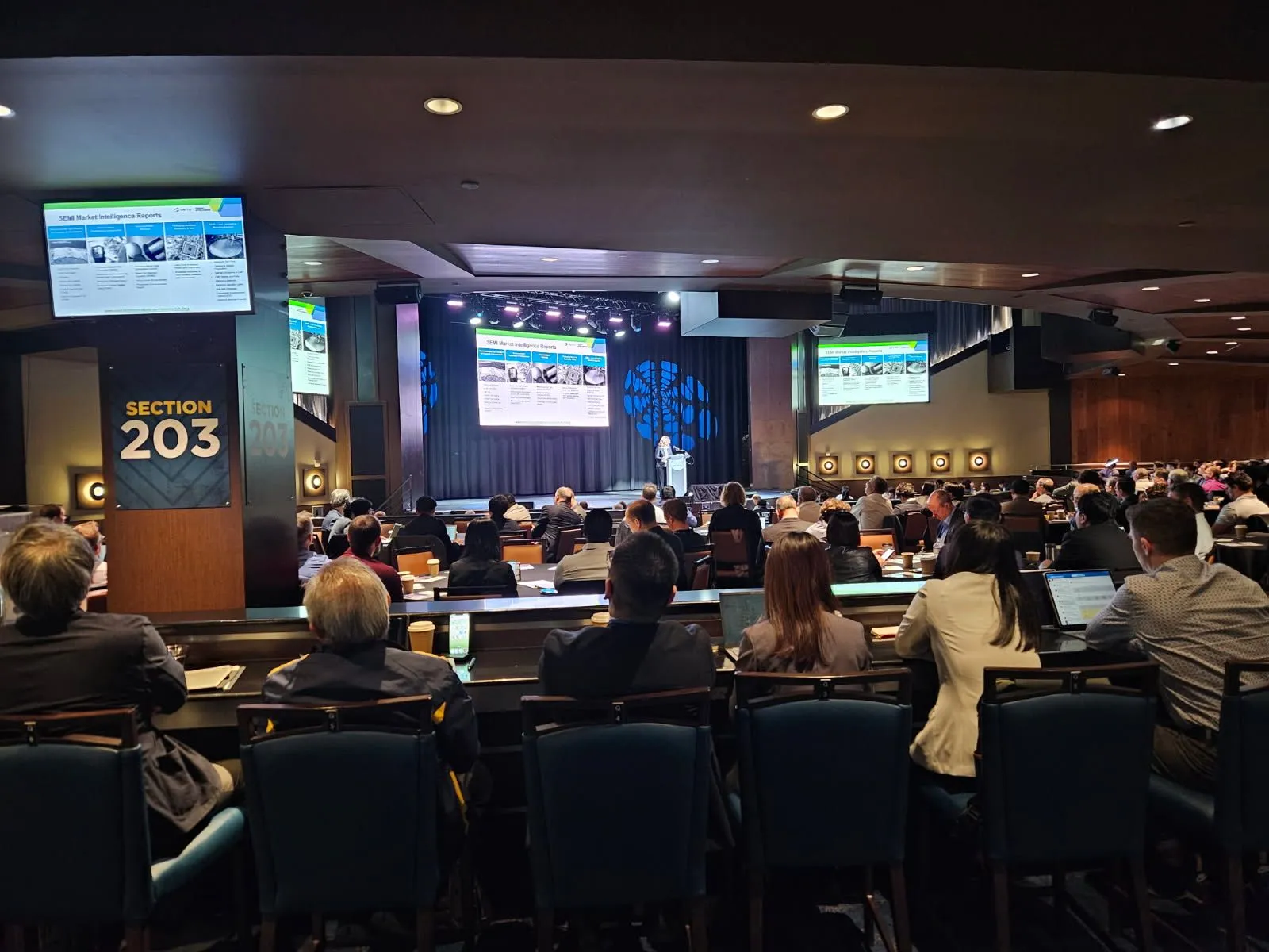
SEMI’s annual Surface Preparation Cleaning Conference (SPCC) brought industry experts to Chandler, Arizona, to address the biggest challenges affecting this area of the semiconductor industry. As the premier technical forum dedicated to advancing surface preparation, cleaning technologies, and wet processes, the conference featured dozens of speakers who shared insights on the current market, emphasizing key themes like advanced packaging, power delivery, advanced DRAM, sustainability, and more.Ahead of this year’s conference, SEMI and Global Net Corp. (GNC) developed a new report, Glass Core Substrate Market and Development Trends, examining manufacturing challenges, supply chain structure, and market outlooks through 2040. This resource helps organizations evaluate the glass core substrate landscape before committing to production. A sample of the report is available for complimentary download. High-Level Updates and SEMI Insights Joe Stockunas, president of SEMI Americas, kicked off SPCC 2026 by announcing that the industry is entering its biggest era yet, on pace to reach $1 trillion in annual revenue in 2026 – 4 years ahead of prior forecast. The semiconductor industry has become the third most valuable global industry with top companies' market capitalization surging over the past decade. By 2030, industry analysts expect annual revenue to soar to $1.9 trillion, driven largely by demand for AI infrastructure, with logic and micro capacity also expected to nearly double. However, Stockunas also noted headwinds including geopolitical tensions and a growing talent shortage.Duncan Meldrum from Hilltop Economics offered a cautionary macroeconomic view, warning that AI growth is now concentrated among a handful of hyperscalers and leading-edge chipmakers, creating concentration risk. Geopolitically driven inflation is squeezing consumers, while supply chain disruptions are impacting critical materials like sulfuric acid, helium, and tungsten. Meldrum also highlighted concentration risk in production, with a few ODMs and manufacturers dominating the AI server market.SEMI analyst Inna Skvortsova provided materials market updates, emphasizing that advanced devices are driving materials intensity per wafer. Lithography, wet chemicals, and CMP are already seeing double-digit growth, led by increasing number of processing steps, rising count of EUV layers, and tightening CMP process windows at advanced nodes. Deposition materials were noted as another fast-growing segment that is forecast to grow at a 13.5% CAGR through 2030, driven by molybdenum adoption and backside power networks. Furthermore, introduction of new materials, including Ruthenium and Tungsten Carbon Nitrite (WCN) hardmasks, brings new opportunities and challenges with regards to wet processes.On memory, Skvortsova confirmed that AI pull has made memory a compute-stack bottleneck, driving capital toward leading-edge logic and HBM. Logic and micro capacity nearly doubles by 2030, but growth is highly concentrated in advanced nodes (≤7nm) pressuring non-AI segments.Skvortsova also highlighted a supply chain shift from globalization to localized production networks, with China emerging as a significant player in areas like bulk wet chemicals, gases, and deposition materials. While alternative sources are emerging, supplier re-qualification may result in higher material costs.Theme 1 - Hybrid Bonding FluxSPCC 2026 highlighted cleaning innovations for hybrid bonding, a core technology enabling AI scaling and glass core substrates. Srini Raghavan (ProSys) presented a paper based on the collaborative work between Intel and ProSys in the area of megasonic removal of flux from narrow gaps in advanced packaging structures. His team found that application of 10 msec pulses of 925 kHz sound wave at 90% duty cycle was very effective in flux removal in a semi-aqueous formulation Acoustic streaming rather than cavitation appears to be the primary cleaning mechanism under the test conditions.Koji Nakata (Kurita Industries) tackled particle contamination, copper corrosion, and chemical consumption in 3D stacking. His solutions include:Functional water + megasonic cleaning for higher particle removal than SC-1.Alkaline water rinsing to reduce copper pad recessing vs. DI water.Functional water to lower chemical consumption, cost, and environmental impact.Theme 2 – Wet Etch, Gate-All-Around, SelectivityTwo presentations highlighted next-gen logic wet etch challenges. IBM's Alma Vela Ramirez showed that an oxide-selective wet chemistry reduced buried void defects by over 20× during dummy gate polysilicon removal in GAA nanosheet flows. From her findings, chemistry 1 showed higher defectivity, while chemistry 2, selective to gate oxide and compatible with spacers, drastically reduced void formation by preserving the bottom oxide layer.Mitsubishi Chemical Corporation’s Tomoki Nara demonstrated a Si/SiGe selective etchant achieving a record 750:1 selectivity, critical for protecting thin SiGe layers during Si thinning in backside power delivery networks (BSPDN). His new alkaline wet etchant and single-wafer spin process address conventional etchants' inability to stop cleanly on SiGe, significantly expanding the process window during Si thinning and reducing the risk of SiGe damage.Theme 3 – Scaling DRAM to Advanced NodesMicron presented two DRAM manufacturing breakthroughs. Shihui (Adara) Yang introduced a dilute sulfuric peroxide clean achieving 3.59× BCF:TCF (bottom container fill and top container fill) selectivity—solving uniformity issues where conventional fluorine-based chemistries etch both layers at similar rates, causing container shorts and yield loss at advanced nodes.Hiroki Uoyama introduced a wafer backside polishing brush incorporating diamond or silicon carbide, achieving over 90% defect height reduction with no wafer thickness loss. This physical cleaning approach improves focus control, alignment accuracy, and overall yield — critical as lithography margins narrow dramatically at smaller nodes.Theme 4 – Sustainable Materials Stripping Solutions Sustainability was another core focus at SPCC 2026, with three distinct approaches taking center stage — each addressing a different facet of environmental impact in the fab.PFAS are among the major pollutants in semiconductor manufacturing waste streams, whose separation and destruction are challenging. As demonstrated by imec’s Sina Kaabipour, representing the collaborative research work between imec, Purdue University, and Enspired Solutions, UV destruction can achieve more than 99% PFAS destruction efficiency for simulated semiconductor manufacturing waste, showcasing great potential for scale-up and direct mineralization from liquid fab waste effluents.Diane Bijou from Technic launched TechniStrip® Micro 680, an NMP-free stripper with sub-2-minute stripping time, better loading capacity, extended bath life, and lower cost per wafer than NMP/amine-based strippers.Chihiro Kobata of JSR unveiled a water-rich stripper removing both photoresist and spin-on glass without NMP, DMSO, and TMAH, at lower temperatures (40–60°C), with ECO conscious, high performance, and high material compatibility and fab-part compatibility.Connect With SEMI SEMI would like to thank all speakers, sponsors, and attendees for the success of SPCC 2026. Download a preview of SEMI and GNC’s new report, Glass Core Substrate Market and Development Trends, and stay connected with SEMI on LinkedIn and X. Clark Tseng is Senior Director of Market Intelligence at SEMI.
Read More
John Barr, Portfolio Manager of the top-ranked Needham Aggressive Growth Fund, is known for his disciplined, long-horizon investment style — a style distinctive enough to earn him a profile in Stock Market Maestros, a book featuring 12 of the world's best investors.Julie Rogers, Executive Director of the ESD Alliance, sat down with Barr to explore his strategies, habits, and investing mindset. For readers in the EDA and semiconductor community, his perspective will feel familiar: Barr spent 14 years in EDA before moving to Wall Street, and he credits that experience as foundational to everything he does today."The EDA industry of the '80s and '90s was an amazing place to learn about technology and business," he says. "Those lessons carry forward."Rogers: How do you stay on top of a changing investment landscape?Barr: I've been managing this Fund for 17 years. I call my investment process "Hidden to Quality Compounders." A “Hidden Compounder” meets four criteria. First, the company has an established business but is investing in something new beyond the typical Wall Street horizon of 12 to 18 months. That requires understanding both the current business and where it's going. Second, the company has the potential to grow five to ten times its current size. Because I invest for the long term — my Fund averages a ten-year holding period — I believe that kind of upside is the only way to reliably beat the market.Third is great management. To me, that usually means founders, family members, or long-tenured executives. I came to that view through my EDA experience. These are people who think long-term and don't veer off course technologically. Finally, I look for availability at a margin-of-safety price — one that reflects the value of the new business or is supported by the balance sheet. Then, I hold while the company transitions and the new business begins to contribute meaningfully.Where do I invest? Broadly defined infrastructure. That starts with technology and manufacturing infrastructure — the tools and products used by engineers — which means semiconductors and data centers, general manufacturing, and traditional infrastructure: concrete, the grid, water, and energy.Defense is another area. Since Russia's invasion of Ukraine, I've thought more seriously about deterrence and the role technology plays in it—autonomous systems, drones, maritime operations, and cybersecurity. Labor is part of this too. The U.S. has a serious shortage of skilled trade workers, and there are publicly-traded skilled-labor trade schools training people to become HVAC technicians, electricians, electrical linemen, welders, auto and aviation technicians. The architecture, engineering, and construction firms that employ those graduates are worth watching.That's my universe: tech and industrials, broadly defined. Finding opportunities means reading conference call transcripts and federal filings, piecing together signals the market hasn't yet recognized. None of it would be possible without my years in EDA.Rogers: It sounds like most of these are small cap stocks.Barr: It's a small cap fund. When I own a small cap stock for ten-plus years and it succeeds, it doesn't stay small. Some of them, anyway.Rogers: Do you hold on at that point, or do they exit the portfolio?Barr: Generally, we hold on. If a position crosses 7.5% of the portfolio, we may trim. If something is off track, we may sell. Once a company crosses the $10–15 billion market cap range — the upper end of small caps — we may opportunistically purchase shares, but generally, we let the position appreciate.Rogers: How do you research a portfolio company’s competition?Barr: The same way: read the transcripts and the filings, and talk to competitors and customers. It's reading, writing, and talking to people — constantly. Everywhere I go, I'm trying to observe what's happening and find connections that may not be obvious.Rogers: As more companies pass the baton to the next generation, how do you build trust in new leadership? Do you develop that second-tier relationship that you had with the founder?Barr: Ideally, I've gotten to know them before the transition. Formally, that happens when companies make their next-tier leaders available to investors. Informally, it happens at trade shows and industry events. The best practice approach is for companies to introduce the heir apparent to the investing community well before any leadership change. That gives everyone time to build a relationship.Rogers: How long does the “Hidden Compounder” stage typically last?Barr: When I invest, these companies are small — market caps of $200 million to $2 billion, often with a single product or business line. They're already investing in the next thing; that's what I'm really investing in. The new business might start contributing within a year or two of my investment, but the company has probably been working on it for two to five years before it crossed my radar.In my experience, about half of my “Hidden Compounders” successfully transition to the next stage. Of those, about half become what I call “Quality Compounders,” which are companies that have clearly hit their stride, like Cadence and Synopsys did years ago.Of that final group, a handful become the big successes — stocks that appreciate between five and 100 times. I have one at roughly 230x since time of first purchase. The full arc, from “Hidden” to “Quality,” can take a decade. Synopsys and Cadence are great examples. Unfortunately, I did not invest in either, despite my background. It's a long-term proposition, and it happens to a minority of companies. But that's exactly where I want to be invested — at the beginning of that journey.Rogers: What's your geographic focus?Barr: The Fund predominantly invests in U.S.-listed companies. But like everything in electronics, it's a global business. Asia matters a great deal. Europe, less so, but you have to know what's happening on all sides.Rogers: Do you have some all-time favorites? Barr: PDF Solutions is at the top of the list. Co-founders John Kibarian and Kimon Michaels have led the company since the beginning and they think in decades, not quarters. I first bought PDF Solutions in 2010 at $4 a share. The Fund is up over 15x on those initial shares.The company has gone through three distinct transitions in that time. We added to our position between 2015 and 2018 as it navigated the loss of Samsung as a major customer and began investing in the Exensio data analytics platform, and its Design-for-Inspection™ contactless E-beam tool. By 2020, those investments started generating returns. In my framework, I still place PDF Solutions in the late “Hidden/early Transition” stage — there's more to come.What makes John and Kimon stand out, beyond their engineering leadership, is their approach to compensation. Since their IPO in 2001, they have never taken a stock option grant — preferring, as their proxy states, to leave those shares for employees and contractors. Their base salaries are a fraction of what comparable small cap CEOs earn. They own substantial stock and rarely sell it. I believe they are building PDF for their customers, their team, their public investors and themselves, in that order. No one else does this. It's extraordinary. I use PDF Solutions as an example of best practice in management compensation and stock ownership.Rogers: What other advice would you have for readers of our blog and individual investors?Barr: Start with Peter Lynch's One Up On Wall Street: How To Use What You Already Know To Make Money In The Market. His core message is to invest in what you know — and your readers know a lot. That's a real edge.Second, be patient. Some people make money through trading and with options, but lasting wealth comes from holding. Have a clear reason for buying and then give it time. Some investments won't work. Some companies will fail. Some will peak and decline. But a few will more than make up for the inevitable mistakes.Third, learn basic financial statement analysis. It doesn't need to be complicated — just enough to navigate an income statement, balance sheet, and cash flow statement. For people in the EDA industry, that's genuinely straightforward. You can teach yourself in about ten hours.And fourth: past performance is not indicative of future results. Things can go wrong. Be careful. Diversify — though if investing isn't your full-time job, you don't need to follow 20 companies. Studies suggest owning around ten, across different industries, captures most of the benefit of diversification.I must add a disclaimer from a compliance perspective that not everything works out and be careful. Consult a financial advisor or expert.About John BarrSince 2010, John Barr has served as Co-Portfolio Manager of the Needham Growth Fund and Portfolio Manager of the Needham Aggressive Growth Fund. He began his Wall Street career in 1995 at Needham Company as a sell-side analyst covering technical software companies. He was named an Institutional Investor All-Star and led a top-ranked software team recognized by Reuters.From 2000 to 2002, Barr was a senior analyst at Robertson Stephens covering semiconductor technology. In 2002, he joined Buckingham Capital Management as a portfolio manager and analyst for a long/short domestic equity hedge fund. From 2009 to 2017, he served on the board of directors of Coventor, Inc., prior to its acquisition by Lam Research. He joined Needham Asset Management in 2009.Before his Wall Street career, Barr spent 14 years in the EDA industry in marketing, sales, and corporate development. In 2020, he co-founded the Wall Street Development Accelerator Internship Program, which introduces students to career opportunities in financial services.Julie Rogers is Executive Director of the ESD Alliance, a SEMI Technology Coalition.
Read More
The semiconductor industry is in one of the largest construction booms in its history, fueled by surging demand for advanced chips, particularly those powering artificial intelligence (AI). AI is fundamentally reshaping both the technology landscape and the infrastructure required to support it. Meeting the construction demand requires collaboration across the semiconductor ecosystem and a strong talent pipeline.What it Takes to Build a Fab Modern semiconductor fabs are complex. These sites include cleanroom fab buildings, central utility plants, electrical substations, wastewater treatment facilities, support buildings, offices and logistics infrastructure.Constructing such facilities requires a highly coordinated, multi-phase approach. Firms like Skanska are typically involved early through design-build models, working alongside owners and stakeholders from the outset. The fab construction process typically has three phases:Core and shell construction, where the structural building is erected and enclosedFit-out, focused heavily on mechanical, electrical and plumbing (MEP) systems Tool installation and utility connection, where the fab becomes fully operational Each phase demands precision and synchronization. A large project can host around 10,000 workers per day—a small town’s worth of activity requiring seamless coordination, logistics planning and rigorous safety protocols.The Workforce ChallengeThe biggest constraint on the semiconductor boom isn’t capital or technology—it’s skilled labor. It’s faced with a shortage of qualified tradespeople, particularly in critical disciplines like electrical and mechanical work.Electricians are in extremely high demand. The rise of both semiconductor fabs and data centers has created concentrated construction activity, where companies compete for the same limited talent pool. But this is not just a numbers problem—it is a challenge of increasing technical skills.Fab construction is far more technical than traditional commercial building. It requires highly trained journeymen and master electricians, pipefitters and welders who understand complex systems and can work in specialized environments such as cleanrooms. Workers must be trained not only in their trade, but also in contamination control, safety protocols and the unique operational requirements of semiconductor manufacturing.Compounding the issue is a generational gap in the workforce. The construction industry is seeing experienced workers retire or leave the field, while the next generation is only beginning to enter the workforce, leaving a shortage of experienced professionals in the middle of the pipeline. At the same time, attracting and retaining next-generation talent is a challenge, as many gravitate toward careers perceived as more analytical, technical and specialized rather than field-based project management work.Ironically, semiconductor construction is exactly that—highly technical, increasingly digital and deeply connected to the future of AI and advanced manufacturing. The challenge lies in communicating that reality and creating clear, compelling career pathways.Beyond Hiring: Building Skills and CapacityOne strategy is to create mentorship models within the trades. Rather than relying on a single large subcontractor to deliver the entire scope—such as electrical work—projects can break the work into smaller packages. This enables multiple firms to participate by pairing experienced trades with newer firms entering the market. These mentor-mentee structures help expand the labor pool while maintaining quality and knowledge transfer. Assumptions about workforce capability cannot be taken for granted. Even when working with established contractors or unions, skill levels can vary by region. This requires more rigorous qualification processes, targeted training and closer oversight, particularly in highly technical areas like MEP systems, which can account for roughly 25% of a fab’s total construction cost.Off-site manufacturing (OSM) is another lever. By prefabricating components in controlled environments, companies can reduce on-site labor demands, improve quality and mitigate workforce shortages. This approach requires tight coordination across the supply chain and early alignment between design, construction and equipment installation teams.Efforts to build the talent pipeline are underway, but many remain localized or in the early stages. In Arizona, for example, Skanska is partnering with community organizations, trade schools and veteran groups to attract new workers into construction careers. Initiatives include job fairs, training programs and “day of discovery” site tours that expose students to real-world projects.Engagement is also expanding to younger audiences. Programs with organizations like the Girl Scouts and STEM-focused institutions are introducing K-12 students to construction and semiconductor manufacturing, helping reshape perceptions and spark early interest.Subcontractor engagement programs are another important component. By supporting small, local subcontractors, companies can broaden participation in the ecosystem while creating new pathways for workforce entry and development, opening capacity for other firms.Subcontractor engagement is not simply a supporting initiative—it is a critical lever for expanding workforce capacity. By intentionally developing and integrating small and local subcontractors into projects, companies can unlock new pools of labor, strengthen regional capabilities and reduce reliance on a limited set of established firms. These efforts create meaningful entry points into the industry, accelerate skill development and enable a more scalable delivery model. When paired with mentorship and structured onboarding, subcontractor engagement becomes a powerful mechanism for both immediate project execution and long-term workforce growth.Yet these efforts are not enough on their own. The scale of the semiconductor boom demands a more coordinated, industry-wide response.A Call for Greater Industry AlignmentEquipment manufacturers, material suppliers and construction firms all share a common customer: the semiconductor manufacturer striving to bring capacity online quickly and competitively. Success depends on how effectively this ecosystem works together.That collaboration must begin early in the project lifecycle. Facilities should be designed with equipment integration in mind, ensuring that tools can be installed efficiently and without rework. Construction schedules must align with equipment delivery timelines. Suppliers must provide clarity on requirements and constraints. All stakeholders must consider how their decisions impact labor demand and workforce readiness.Equally important is a shared commitment to workforce investment. This includes:Developing standardized training programs for semiconductor construction Expanding apprenticeship and mentorship models Partnering with educational institutions and community organizations Promoting construction as a high-tech, future-oriented career path Leveraging innovation, such as OSM, to optimize labor utilization Building the Future TogetherThe semiconductor fabs being built today will underpin the technologies of tomorrow—but these facilities do not build themselves. They require thousands of highly skilled, specialized workers who operate in sync and are supported by a network of companies that must collaborate more closely than ever before. This is the time for the semiconductor value chain to operate as an integrated ecosystem rather than a series of isolated players. Through shared commitment to workforce development, collective responsibility and sustained investment in talent, the industry has the opportunity not just to meet demand, but to fundamentally shape the future of advanced manufacturing.Joycelyn Yue is National Director - Subcontractor Engagement at Skanska, where she leads a team of professionals in 23 offices. Yue partners with regional and national leadership to further develop and elevate the company’s Supplier Diversity Compliance program. In her role, Yue maximizes opportunities for small and diverse businesses while establishing relationships with the communities where Skanska builds.Yue joined Skanska from Southern California Edison where she served as Supplier Diversity Senior Program Manager. Yue has a B.S. in Business Management from California State Polytechnic Pomona and is based Los Angeles.
Read More
The SEMI Startups for Sustainable Semiconductors (S3) program, now in its 5th year of inviting startups to apply, is pleased to announce the 33 startups chosen to move to the semifinalist virtual pitch event happening July 29-30. From this pool, 10-12 finalists will be selected and invited to pitch to a live audience at SEMICON West 2026 in San Francisco, October 13-15, 2026. The committee, made up of experienced Corporate Venture Capitalists (CVCs) from the global semiconductor industry, received impressive submissions in all four categories for 2026:Decarbonized Semiconductor ManufacturingDesign for Sustainability – Chips PackagingDatacenter Efficiency in Power Delivery and ThermalsNew Frontiers in Sustainable ComputingLed by Micron this year, the program’s strongest feature is the exposure to the CVCs, as well as the personal mentoring each semifinalist receives. The mentoring topics are tailor-made to align with the greatest need of the startup and can range from a basic introduction to semiconductor manufacturing, to connecting them to funding sources. A full analysis of the program kicked off this year’s efforts and is captured in a report available here.The program saw an increase in quality applications with a geographically diverse group of semifinalists who will all share their solutions for the building and use of more sustainable electronics. Are you an investor and would like to receive notice of the virtual and live pitch events around S3? Register your interest here. 2026 S3 SemifinalistsAikido TechnologiesSan Francisco, CA, USAAikido Technologies is building clean, marine datacenters - AI-grade compute on the ocean, built faster, cheaper and more efficiently than conventional infrastructure. Axonal NetworksMontreal, QC, CanadaAxonal Networks develops digital photonics technology (paraLITE™) that performs computation directly in silicon photonics. Our devices eliminate electronic bottlenecks, enabling ultra-high-speed, energy-efficient computing for AI infrastructure and next-generation semiconductor systems. C1 BioChicago, IL, USAC1 Bio is building a biomanufacturing platform that converts low-cost agricultural waste into high-performance photoresist materials for semiconductor manufacturing. Our initial product, bio-based 4-acetoxystyrene (ASM), is a drop-in replacement for petroleum-derived monomers, enabling sustainable, domestic production of critical lithography materials without compromising cost, purity, or performance. CHIPADD, Corp.Binghamton, NY, USACHIPADD is the first to additively manufacture ultra-efficient copper cooling features directly onto the surface of GPU, CPU, and other high power silicon chips. The company’s innovation includes materials and methods for robust bonding, manufacturing of solid and porous cooling features, enhanced materials for cooling, manifold and precision jet design. EMTAR Technologies IncRichmond, VA, USAEMTAR Technologies designs highly integrated beamforming SoCs and RF front-end ICs for 6G non-terrestrial networks. Our chips enable low-latency, high-throughput satellite communications while reducing power consumption and hardware complexity, improving energy efficiency of satellite communication infrastructure. enaDyneLeipzig, Saxony, GermanyenaDyne builds a fully electric, modular abatement system for semiconductor fabs based on non-thermal plasma catalysis. Our reactor destroys PFCs, VOCs, and NOx at 99% DRE through electron-impact chemistry at near-ambient temperature, fitting the same footprint as burn-wet for direct drop-in replacement. Same hardware extends to electrified chemical synthesis. FlexcomputeBoston, MA, USAFlexcompute builds a GPU-native physics simulation platform: Tidy3D (photonic/electromagnetic FDTD), PhotonForge (photonic design automation), Flexcompute RF (full-wave EM), and Flow360 (CFD/thermal), delivering results 50-500x faster than legacy CPU tools. FlexAgent, our AI assistant, enables engineers to run and iterate simulations via natural language, accelerating chip and data center component design. Floadia CorporationTokyo, JapanAI data centers are consuming large power. This is a global issue. Floadia developed analog CiM (Computing in Memory) technology that execute AI matrix calculation at 1/1000 power of digital way to solve AI data centers power issue using unique memory technology. FS2Saint Louis, MO, USAFS2 is developing a revolutionary Monolithic 3D (M3D) integration platform and memory. We are building next-generation stacked 3D SRAM and Process-on-Memory (POM) architectures. Our product delivers memory solutions with superior bandwidth, capacity, low latency, high energy efficiency, and lost cost for AI workloads. HEXAspec IncHouston, TX, USAHEXAspec develops advanced molding compounds for semiconductor encapsulation using high-aspect-ratio hexagonal boron nitride (hBN) nanosheets in polymers. Its scalable, patent-protected exfoliation process enables 10x — higher thermal conductivity while maintaining electrical insulation, mechanical strength, and compatibility with standard OSAT and foundry packaging for HPC, automotive, and edge-AI applications. IL-BSC TechnologiesBrooklyn, NY, USAHelium-free wafer thermal stabilization system for electrostatic chuck applications. Replaces helium backside cooling with low-vapor-pressure ionic liquid thermal fluid, tier-specific chemical getter, dual-mode acoustic purge, and plasma-resistant barrier integrity sensor. Eliminates dependence on critical helium supply while maintaining thermal uniformity required for advanced node semiconductor manufacturing. IWI Australia Pty LimitedSydney, NSW, AustraliaWe have developed and piloted a patent-pending catalytic quench of hydrogen peroxide (CQ) in fab wastewater, especially in complex water matrix with high peroxide load, extreme acidity and heavy metal. We have also developed a patent-pending oxidation process for triazole, another pain-point of fab operation and water reuse. K1 SemiconductorChicago, IL, USAAt K1 Semiconductor, we create engineered semiconductor wafers by peeling thin layers from high-quality single-crystal “parent” wafers. Our patented wafer splitting method releases a 5-50 micron-thick layer of single-crystal material from the parent wafer, which is then transferred and bonded to a handle wafer to create a custom semiconductor wafer. KoolMicro, Inc. Dongtan, Gyeonggi-do, South KoreaKoolMicro is engineering the "Thermal Highway" for the AI era. We develop Integrated Manifold MicroChannel (IMMC) modules that handle 4,000W+ thermal loads. Our Direct-to-Chip solution utilizes vertically sprayed coolant to remove heat directly from the chip level, ensuring next-gen GPUs and CPUs never throttle. NanoPattern Technologies, inc.Chicago, IL, USAAt NanoPattern, we are commercializing a photodefinable hardmask (PDH) liquid formulation for advanced semiconductor packaging. Our resin-free, sustainable, metal-oxide formulation enables the use of non-photosensitive polymer dielectrics to form sub-micron lines and vias for high-resolution RDLs. We eliminate expensive vacuum deposition tools, drastically improving design freedom for next-generation AI chips. NicslabRochester, NY, USANicslab develops advanced electronic and photonic control systems that enable precise testing, operation, and deployment of photonic integrated circuits and semiconductor devices. Its platforms replace complex lab equipment with scalable, software-driven solutions, helping transform photonics from research into reliable, real-world applications across AI, data centers, quantum technologies, and advanced sensing. NordAmpsLund, Skåne County, SwedenNordAmps develops ultra‑high‑performance RF circuits using vertical III‑V nanowire transistors on standard silicon. The architecture delivers higher frequency performance, lower power use and smaller footprint than GaAs, GaN or SiGe, while being fully compatible with existing semiconductor fabs for true scalability. Normal ComputingNew York, NY, USANormal EDA is a purpose-built AI platform for semiconductor design that applies auto-formalization, combining LLMs with formal logic, to accelerate chip design and prove correctness. Deployed with half of the top ten semiconductor companies by revenue, and used to design our silicon: CN101, the world's first thermodynamic computing chip. NSS WaterGothenburg, Västra Götaland County, SwedenAt NSS water we are building a solution to drastically decrease water and chemical use in semiconductor industry and doing advanced solvent reclaim of downstream waste from rinse processes such as wafer cleaning, etch and more. With our new patent technology we can do IPA-reclaim and produce extremely pure water Plaid SemiconductorsAtlanta, GA, USAPlaid is building a modular platform that enables rack-on-package integrating large numbers of AI processors onto a single package. By collapsing distance within systems, we deliver higher bandwidth, lower power loss, and dramatically improved performance for next-generation AI infrastructure. Power to HydrogenColumbus, OH, USAPower to Hydrogen is building industrial-scale AEM electrolysers that reduce the stack costs by 65% for clean hydrogen production. For semiconductor manufacturing, we are developing a pathway from a 10 kW pilot to a 500 kW fab-ready module for onsite, ultra-high purity, low-carbon hydrogen production. Powerlattice Technologies Inc.Phoenix, AZ, USAThe first true monolithic integrated voltage regulator designed for high wattage ( 1kw) ASICs and XPUs. Project LegacyLondon, England, United KingdomA neuromorphic semiconductor for autonomous systems (robotics). Our chip architecture consists of neurons taken from the 7-brain regions within neuroscience. This will allow for predictive learning and tasks to occur once a software algorithmic layer is applied. We see current neuromorphic hardware layers as the problem. Rise Technology srlMilano, Lombardy, ItalyRiseTech develops next-generation semiconductor equipment based on its proprietary Dynamic Drop™ technology, overcoming the limits of conventional electroplating. The platform enables high-uniformity, high-throughput formation of interconnects, improving yield and enabling advanced architectures in heterogeneous integration, including chiplets, DRAM stacking, and 2.5D/3D packaging. SolidT Technologies LtdPetach Tikva, Central District, IsraelSolidT develops thin-film thermoelectric solutions enabling localized, active thermal control in semiconductor systems. Our technology mitigates hotspots, reduces thermal gradients, and improves efficiency and reliability. It integrates at chip or module level alongside existing cooling systems, supporting high-performance computing and advanced semiconductor applications. Stellar Engiine Milpitas, CA, USAInnovation is plasma chemistry creation, 100 C, atmospheric to vacuum pressures, with significantly lower energy than legacy RF and microwave methods. Product is plasma reactor and pulsed high voltage generator controlled by advanced recipe algorithms. Applications are PFC abatement, followed by NF3 chamber cleaning, advanced packaging surface conditioning and PEALD. Supra Elemental Recovery, Inc.Austin, TX, USASupra is a technology startup addressing the key chokepoint in the global critical minerals supply chain: element-specific separation. While existing technologies struggle to separate individual minerals at high-purity—leading to inefficient and expensive processes—Supra is building an affordable and effective solution. TopoLogic Inc.Tokyo, JapanWe are developing a high-speed, high-capacity memory design IP technology, that can be directly embedded to CMOS based processors. It is capable of 1~2ns write speeds, and be 5~10x high capacity compared to conventional SRAM technology, based on a material innovation to conventional MRAM platform. UNISERSZurich, Canton of Zürich, SwitzerlandUNISERS has developed a novel wafer defect inspection and characterization technology to help fabs find and identify minute contaminants (sub 10nm), which are mostly invisible to currently used inspection equipment. As transistor nodes move to 3nm and below, these very small particles cause huge yield issues in state-of-the-art wafer fabs. VEIR, IncWoburn, MA, USA Superconducting power solutions (cables and supporting infra). From grid to rack. Wise IntegrationFranceWise-Integration digitalizes power converters to overcome power limitations for AI data center and electrification. We build smaller, faster and more efficient AC/DC and DC/DC converters by combining WiseWare®, a 32-bit digital controller, and WiseGan®, a digital-first GaN power IC, enabling smarter regulation, higher power density and reduced system complexity. xMEMS LabsSanta Clara, CA, USAWe are building µCooling, a novel active thermal management solution for high-density data centers. We provide precision active cooling that targets severe component hot-spots directly. Acting as a third cooling option beyond liquid and fans, it maximizes density and minimizes complexity, covering SSDs, VRMs, optical transceivers, and DIMMs. YPLASMAMadrid, Community of Madrid, SpainYPlasma develops solid-state ionic wind cooling using Dielectric Barrier Discharge (DBD) plasma actuators—no moving parts, silent, and ultra-thin. Our technology replaces fans in Edge AI devices, data centers, and high-performance electronics, delivering targeted airflow with higher reliability, lower acoustic signature, and form factors impossible for mechanical cooling. Kenneth Guertin is Program Manager, Operations at SEMI.
Read More