downloadGroupGroupnoun_press release_995423_000000 copyGroupnoun_Feed_96767_000000Group 19noun_pictures_1817522_000000Member company iconResource item iconStore item iconGroup 19Group 19noun_Photo_2085192_000000 Copynoun_presentation_2096081_000000Group 19Group Copy 7noun_webinar_692730_000000Path
Skip to main content
Cybersecurity vulnerabilities within the semiconductor supply chain are a growing concern, ranging from individual threats to whole supply chain cyber resilience. It is imperative that the semiconductor industry addresses these risks. Last year, the Semiconductor Manufacturing Cybersecurity Consortium (SMCC) at SEMI introduced Semiconductor Supplier Cybersecurity Assessment (SSCA), providing a streamlined framework allowing suppliers to complete one standardized questionnaire to comply efficiently. The assessment process involves suppliers presenting evidence to support their claims of security controls and measures put in place. Such a body of evidence is critical to establish confidence in the suppliers’ ability to manage risk and comply with standards. The SSCA is a free, open-access resource for the semiconductor industry. This is intentionally made openly available to support SMCC’s mission to strengthen cybersecurity across the semiconductor manufacturing ecosystem. The questionnaire aligns with the six functions of the National Institute of Standards and Technology (NIST) cybersecurity framework 2.0: Govern, Identify, Protect, Detect, Respond and Recover. A recent project led by Swansea University’s Systems Security Group (SSG), in close collaboration with SEMI SMCC, is mapping the evidence requirements necessary for SSCA assurance. The project is funded by the UK Research and Innovation (UKRI) as part of seed funding to support UK/US/Germany collaborative research and innovation projects in the field of semiconductor security. UKRI supports such collaboration in the interest of “maintaining confidence in security throughout the design and manufacturing processes,” and particularly to support research addressing “what tools and techniques could help to reduce the risks associated with third-party hardware design and manufacturing services?”.The project ensures that the global ecosystem is engaged so that evidence requirements developed are acceptable, cost-effective, in line with the latest standards and practice, and ultimately suitable for adoption. As part of this project, two workshops are being organized, one in Germany at Bavarian Chip Alliance, Nuremberg on Tuesday, March 10 and one in the UK at Swansea University on Thursday, March 12, aiming to introduce SSCA and the evidence requirements, gather feedback and inspire early adoption. Join either of these workshops to help shape the evidence requirements and help prepare for effective supply chain security assurance. Participants must download the SSCA framework prior to the workshop.Register for the Germany Workshop on March 10Register for the UK Workshop on March 12Key TopicsIntroduction to Semiconductor Manufacturing Cybersecurity Consortium (SMCC)Standardized Semiconductor Cybersecurity Assessment (SSCA)Supply chain assurance and evidence mappingGroup discussion to feedback on evidence requirementsOpen Q A with cybersecurity and compliance expertsWho Should AttendCybersecurity and compliance professionalsSemiconductor suppliersLegal and regulatory affairs professionalsFabless chip designers and foundriesTesting, packaging, design software, R D tools and IPManufacturing/assembly equipment and ancillary fab servicesIntegrated device manufacturersAbout the authors:Siraj Shaikh is a Professor in Systems Security at Swansea University (UK). His research interests lie at the intersection of cybersecurity, systems engineering, and computer science addressing cyber-physical systems security for automotive and transport systems. He is also Co-Founder and Chief Scientist at CyberOwl, which is dedicated to risk analytics and security monitoring for the maritime sector.Mayura Padmanabhan is a Technical Project Manager at SEMI who manages the Cybersecurity Technology Coalition and Traceability activities.
Read More
Every time a transistor switches, it generates heat. Pack enough transistors together and you hit a wall: the chip melts before it computes. This thermal ceiling is why Splunk notes that "as physical and economic limitations are reached, the pace predicted by Moore's Law is slowing."Light solves this problem. Photons carry information without generating heat. Semiconductor Engineering details how heat dissipation and bandwidth bottlenecks make optical solutions the only viable path forward.But photonics introduces a different problem. Silicon has an indirect bandgap, which means it cannot emit light efficiently enough to produce lasers. Building photonic systems requires III-V compound semiconductors like indium phosphide (InP) and gallium arsenide (GaAs). These materials come with manufacturing constraints: InP substrates remain limited to 150mm, and GaAs wafers top out at 150mm, while silicon runs at standard industrial diameters of 200mm or 300mm. You cannot build a complete photonic system on silicon alone, so heterogeneous integration becomes mandatory. The result is that chief technology officers (CTOs) now manage two incompatible material systems, doubling technical complexity and supply chain risk.How Different Regions Are RespondingUnited States Intel has shipped 8 million photonic chips with 32 million integrated lasers. But the move that matters most is NVIDIA adopting TSMC-Broadcom co-packaged optics in its 2025 GB300 chips. When the dominant AI hardware company makes an architectural choice, competitors either follow or lose relevance.EuropeEuropean companies are solving their scale problem through consolidation. The market grew from €124.6 billion (2022) to a projected €175 billion (2027). Between January and June 2025, EPIC recorded 125 transactions worldwide, with European companies leading 50 of them. ZEISS established a new strategic business unit with €200 million in annual revenue across 6 countries. The strategy is to build on existing strengths in materials science and precision manufacturing.ChinaChina is building a parallel system designed for self-sufficiency. CHIPX produces 6-inch lithium niobate wafers with 110 GHz bandwidth, built despite U.S. export controls. This aligns with national policy: Xi Jinping chaired a February 2023 Politburo session focused on "basic research for self-reliance in science and technology." Optics Valley now hosts 5,000+ high-tech companies, targeting self-sufficiency within 4 years.Asia-PacificJapan, Taiwan, and India are combining strengths rather than building everything domestically. Japan committed $25.7 billion to semiconductor development between 2022 and 2025, and TSMC opened its first overseas R D facility there. India offers up to 50% capital support for photonics fabs and contributes 20% of global chip designers.The Next DecadeMarket projections vary wildly because the category spans everything from mature LED lightbulbs to emerging quantum computing systems. Mordor Intelligence projects growth from $1.75 trillion in 2025 to $2.39 trillion by 2030, while MarketsandMarkets forecasts $1.09 trillion to $1.48 trillion. This uncertainty matters because executives must commit billions in capital to technologies with decade-long development cycles.2025-2026The near-term focus is power efficiency. Traditional pluggable optical modules create 22 decibels of signal loss, requiring 30W per port to compensate. Co-packaged optics cuts power consumption by 3.5x. Ayar Labs' TeraPHY will deliver 8 Tb/s using UCIe standard packaging. In automotive, entry-level LiDAR drops to $200.2027-2032Quantum photonics moves from laboratory to commercial deployment. The market grows from $850 million in 2025 to $3.78 billion by 2030, with PsiQuantum partnering with GlobalFoundries to develop million-qubit systems by 2027. Unlike superconducting qubits requiring near-absolute-zero cooling, photonic qubits function at room temperature.2032-2035+The quantum market reaches $17.4 billion by 2035. Architectures combining analog, digital, quantum, photonic, and neuromorphic computing will require new transducer technologies, which means CTOs can no longer specialize in a single computing paradigm.Energy demand accelerates all of this. Data center electricity consumption will reach 945 TWh by 2030, and photonics can reduce that by over 50% by 2035.What This Means for LeadershipEach executive role faces a distinct version of the same problem: making decisions now about technologies that won't mature for years.Chief Executive OfficersCEOs face timing decisions with no clear answer. Adopt co-packaged optics in 2025-2026 and risk immature technology. Wait until 2028 and watch competitors capture market share. Japan's $25.7 billion commitment means smaller firms now compete against sovereign capital.Chief Technology OfficersCTOs must hold technical depth across incompatible domains. Silicon photonics, III-V materials, and thin-film lithium niobate each require different knowledge bases and supply chains. Most engineers specialize in one; photonics CTOs need working knowledge of all three while balancing 15-year development cycles against 2-year product roadmaps.Chief Financial OfficersCFOs must model returns on infrastructure that doesn't exist yet. The 50% power reduction from photonics changes total cost of ownership calculations, but boards need convincing before savings materialize.Corporate Boards Boards face a knowledge gap that affects governance quality. Most members don't understand why quantum-neuromorphic-photonic convergence matters at the business level. Leadership transitions signal consolidation is underway: IPG Photonics replaced its CEO in June 2024, Lumentum in February 2025.The Leadership ProblemFinding people who can run photonics companies is difficult because the field barely existed a decade ago. The technical knowledge lives in research labs. The business experience lives in traditional semiconductors. The people who combine both are rare.The broader market reflects this scarcity: over 330 R D vacancies appeared in the first half of 2025 alone. When technical roles are that hard to fill, executive searches require a global reach that most firms lack. In our searches, we regularly build single leadership teams by recruiting across China, Romania, Russia, the U.S., Germany, France, the UK, and India.The companies that figure out leadership first will have an advantage that compounds over years.About the AuthorsJan-Bart Smits is a Managing Partner at Stanton Chase Amsterdam. He serves as Global Subsector Leader for the Semiconductor industry and holds an M.Sc. in Astrophysics from Leiden University. David Harap is a Managing Director at Stanton Chase Austin with over 25 years of executive search experience. A Cornell University graduate and Father Kelly Scholar, he lectures at the University of Texas at Austin.
Read More
On December 13, SEMI submitted its response to a Request for Information (RFI) from the U.S. Department of Commerce (the Department) regarding the newly launched American Artificial Intelligence (AI) Exports Program. The intent of this program is to position U.S. firms as global leaders in AI by connecting them with international buyers, leveraging the Department's export promotion tools and supporting industry-led consortia through targeted government backing. By issuing this RFI, the Department intends to solicit input on the development of industry-led consortia capable of delivering full-stack American AI export packages under the American AI Exports Program. Working with member companies, the SEMI Public Policy and Advocacy (PP A) team developed a response highlighting the importance of the semiconductor supply chain to the AI ecosystem, and offering various recommendations for consortium formation, federal support, strategic objectives, and proposal evaluation. The response was informed by direct discussions between SEMI PP A and Department officials implementing the program. Some of the key aspects of SEMI's response include the following:Broader AI Tech Stack Definition: The Department should recognize semiconductor manufacturing technologies, mature node semiconductors, and energy/environmental control systems as foundational elements of the AI technology stack. Evaluation Framework: Evaluation criteria for consortium proposals should align with CHIPS for America requirements and guardrails, focusing on national security, economic competitiveness, and commercial viability, as well as infrastructure needs.Consortia Governance: Consortia should be industry-led and feature: honest brokers capable of coordinating commercial actors while advancing national interest objectives; modularity to ensure that the various technology layers function as distinct yet interoperable units; and clear frameworks for intellectual property protections and regulatory compliance. Foreign Participation: Vetted foreign entities should be allowed to participate in the program in order to reflect the global nature of the AI ecosystem and to strengthen allied and partner nation supply chain resilience.Federal Support Mechanisms: The Department should leverage the unique capabilities of the National Institute for Standards and Technology, Center for AI Standards and Innovation, Bureau of Industry and Security, Export-Import Bank, Development Finance Corporation, and others, including expedited licensing, financing tools, tax incentives, and interagency liaisons to accelerate exports. National Security Compliance: SEMI's comments emphasize robust compliance programs, cybersecurity, supply chain security, and risk-based licensing to prevent misuse or diversion of AI technologies. Global Competitiveness and Standards: SEMI urges rapid implementation, international promotion of U.S. AI technologies, and leadership in global standards to ensure interoperability and trusted adoption worldwide.SEMI is grateful for the feedback provided by our member companies in developing this comprehensive response to the Department's RFI. Visit SEMI Global Advocacy to learn more about public policy efforts and developments as well as how your company or organization can get involved.Ben Kallen is Sr. Manager, Public Policy Advocacy at SEMI.
Read More
2025 was a milestone year for the Semiconductor Manufacturing Cybersecurity Consortium (SMCC). Across standards development, industry collaboration, and community engagement, the SMCC major advancements strengthened cybersecurity across the global semiconductor supply chain.From new guidance documents to standing-room-only conversations at SEMICON West, the past year demonstrated what’s possible when industry, government, and technology leaders come together with a shared mission: protecting one of the world’s most critical industries.More Than Just Standards: 2025 SMCC Created Key Assets One of the most significant accomplishments of the year was the release of the SEMI E187 Compliance Guidance Document. This new resource provides supplemental guidance, rationale, and example artifacts for all twelve E187 Standards requirements, helping organizations more clearly understand what good cybersecurity practice looks like in real-world semiconductor environments.In September, SMCC introduced the Semiconductor Supplier Cybersecurity Assessment (SSCA), a streamlined framework that allows suppliers to complete one standardized questionnaire showing their level of cybersecurity and share results with multiple customers thereby reducing compliance burden and improving efficiency. With the SSCA, suppliers can complete one standardized questionnaire and share results with multiple customers, cutting down on redundant requests while improving consistency and efficiency.Both the SEMI E187 Compliance Guidance Document and the SSCA are free resources for anyone in the industry. These assets were intentionally made openly available. SMCC’s goal is to strengthen cybersecurity across the ecosystem, not to profit from it. By enabling broad adoption, these resources are designed to deliver collective benefits and accelerate progress for everyone.SMCC also collaborated with NIST through the development of the NIST CSF 2.0 Semiconductor Manufacturing Profile. The profile completed its public comment period in July and helped align semiconductor manufacturing needs with the latest version of the NIST Cybersecurity Framework.Cybersecurity Takes Center Stage at SEMICON WestJennifer Lynn from IBM shares her insights about the NIST CSF 2.0 semiconductor manufacturing profile during the Cybersecurity Forum.Cybersecurity was front and center at SEMICON West, where SMCC’s Cybersecurity Forum drew more than 100 attendees from across the semiconductor ecosystem. The program featured a strong lineup of speakers from device makers, equipment suppliers, cybersecurity firms, and government agencies, covering topics such as supply chain assurance, fab equipment security, vulnerability management, and regulatory trends.Poster Presentations at the Cybersecurity ForumThis year also marked a first for SMCC with the inaugural Cybersecurity Poster Presentation, showcasing innovative work from more than 10 companies and academic contributors. The session created space for deeper technical conversations and highlighted the breadth of thinking across the community.The event would not have been possible without the generous support of the Cybersecurity Forum sponsors: Applied Materials, Fasoo, PEER Group, Seclore, Tokyo Electron, and TxOne Networks. Their commitment underscores the growing recognition that cybersecurity is a shared responsibility.Celebrating the People Behind ProgressAt the heart of SMCC’s success are the volunteers who dedicate their time and expertise to advancing the consortium’s mission. A special Leadership Excellence Award was presented to Doug Suerich (PEER Group) in recognition of his exceptional contributions and lasting impact on SMCC’s work.During the forum, we awarded several Working Group members for their outstanding contributions:SZ Lin (Sun Square) receiving a certificate of merit for his contributions to SMCCAnu Machavarapu (ASML)Anusha Annapareddy (Applied Materials)Donato Kava (Advanced Energy)Jared Buckley (Texas Instruments)Mashiro Supika (Tokyo Electron)Pradeep Kumar (Lam Research)Ryan Daniel (PEER Group)SZ Lin (Sun Square)TxOne NetworksWe also honored the leadership and commitment of our Working Group Chairs, whose guidance and persistence continue to shape SMCC’s direction:Albert Fuchigami (PEER Group), Andrew Seward (Tokyo Electron), Bill Higgs (ASML), Daniel Platea (ASML), Dave Dunne (Applied Materials), Eiji Hagio (Tokyo Electron), Jennifer Lynn (IBM), Kim Daich (PDF Solutions), Konstantinos Papapanagiotou, Leon Chang (TSMC), Lori Kessler (Applied Materials, Retired), Mike Tanori (Intel Foundry), Quentin Ellis (PEER Group), Ryan Bond (Intel Foundries), Sukwon Kang (Applied Materials), Wilko Baks (ASML), and Youngwoo Son (SK Hynix).Looking AheadAs we close out 2025, we extend our sincere thanks to all SMCC volunteers, Working Group Chairs, forum speakers, poster presenters, sponsors, and the SMCC Governing Council. Your dedication continues to move the industry forward and strengthen cybersecurity across the semiconductor landscape.If you’re interested in getting involved in SEMI’s cybersecurity activities, we’d love to hear from you. Please contact Mayura Padmanabhan at [email protected] to learn more.
Read More
Advanced packaging is no longer operating behind the scenes. The technology of advanced packaging is helping to sustain the speed of the semiconductor industry’s improvement in power and performance, even as the Moore’s Law roadmap for wafer-level scaling comes under strain.At the Advanced Packaging Conference during SEMICON Europa 2025 in Munich, global experts examined the growth trajectory of this critical sector and Europe’s potential to lead in next-generation packaging solutions.Market Momentum Fueled by AI and HPCRomain Fraux, Chief Research Officer at Yole Group, forecasted that global revenues for advanced packaging will grow from $46.1 billion in 2024 to $79.4 billion by 2030. “Everything is linked to AI and high-performance computing (HPC),” said Fraux, while also emphasizing the growing relevance of automotive applications in driving demand.Romain Fraux, Chief Research Officer, Yole GroupThis demand is accelerating innovation across the supply chain. One emerging area is panel-level packaging, which breaks away from traditional round wafers. As Andreas Wocko, Sales Manager at Lam Research, observed, “Since the 1970s, the semiconductor industry has built on wafers. Now we are not just scaling, we are reshaping, building in a square format for the first time” – an innovation which substantially increases area efficiency and reduces device cost. Andreas Wocko, Sales Manager Europe, Lam ResearchTechnology Transformation from Lab to FabEurope is already investing in the foundational technologies that will power tomorrow’s packaging systems. Rolf Aschenbrenner, Deputy Director of Fraunhofer IZM, the home of the European Union’s APECS advanced packaging pilot line, discussed ongoing research into functional interposers, routing density, and organic interposers. “Our goal is to show how a new design philosophy incorporating chiplets can be brought to the industrial systems level,” said Aschenbrenner.Rolf Aschenbrenner, Director Deputy, Fraunhofer IZMThese breakthroughs are essential, as pitch sizes shrink and new materials emerge. Dr. Jessica Stubbe, Global Application Manager at MKS Atotech, described how interconnect densities have doubled in the past two years, with the industry moving to pitch sizes of less than 10µm. Stubbe said this new technology “will be enabled by a move from traditional solder-based interconnects to copper-to-copper hybrid bonding to provide higher density I/Os and lower resistance.” Jessica Stubbe, Global Application Manager, MKS AtotechInnovation Meets Real-World IntegrationThis increased density carries thermal risks with it. As Ram Trichur, Global Head of Semiconductor Packaging at Henkel Corporation, said, “New architectures enabled by advanced packaging are putting power devices on the backside, interposer or substrate, and this addition of more power delivery components in the package creates more local hotspots.”The reduced feature sizes inside the latest packages make it more difficult than ever to apply thermal interface materials. “At Henkel, we are now making 1µm-level fillers which enable the effective filling of gaps as small as 7µm,” said Trichur.Ram Trichur, Global Head of Semiconductor Packaging Market Segment, Henkel CorporationOne of the applications which stands to gain the most from the development of advanced packaging technology is silicon photonics. Dr. Himani Kamineni, Director for Advanced Packaging at GlobalFoundries, described how co-packaged optics (CPO) brings photonics directly inside the package, reducing connection lengths from centimeters down to millimeters, and providing higher bandwidth and lower latency at lower power. “Advanced packaging and CPO are foundational elements for AI and data centers to enable scalability to the next generation of compute,” said Kamineni. “But it will need a lot of packaging innovation: silicon interposers, copper-to-copper interconnects, and fiber-attach units for precise alignment.” Himani Kamineni, Director, Advanced Packaging, GlobalFoundriesReliability and Test Under PressureIn the transition to new packaging technology, it is crucial that the industry does not lose sight of the reliability standards which have made semiconductors so valuable in sectors such as automotive and aerospace. Amar Mavinkurve, Director of Materials and Labs Package Innovation at NXP Semiconductors, warned the finer spacing and smaller feature sizes in the latest packages posed a problem for reliability and long-term performance. He said, “We are dealing now not just with one failure mechanism, but with multiple. So, the way that we are used to describing behavior in models will not necessarily hold in future. Even industry standards might not hold.”Discussing new technologies such as copper-to-copper interconnects, Mavinkurve pointed out that failure would not be due to a single event, but to processes such as electromigration, corrosion, and thermomechanical effects. To model reliability properly in future, he said, “we need to move from a physics of failure to a physics of degradation.” Amar Mavinkurve, Director Materials and Labs Package Innovation, CTO, NXP SemiconductorsFabio Pizza, Business Segment Manager at Advantest Europe focused on quality and failure. With geometry scaling toward 1nm, early identification of known-good dies is essential to optimize cost and test coverage. Pizza said that, while device manufacturers need to keep time-to-market and the cost of test under tight control, they are also trying to figure out how to increase test coverage. “In a modern GPU, even a 100 DPPM quality process leaves 20 million transistors untested,” he said. Fabio Pizza, Business Segment Manager, Advantest EuropeEurope’s Position in the Global EcosystemThe conference concluded with a panel discussion about the prospects for Europe in the global advanced packaging market. According to Yole’s Romain Fraux, there is a strong ecosystem in Europe: “Europe’s strengths include specialized packaging service providers in the photonics and power market segments, as well as many packaging equipment manufacturers,” said Fraux. This resonated with the instincts of NXP’s Amar Mavinkurve and Advantest’s Fabio Pizza. Mavinkurve said: “We should focus on what we are already good at doing. It will be challenging to compete with advanced packaging providers elsewhere for AI and HPC business.”Ram Trichur of Henkel, however, urged the industry in Europe, “Do not take your foot off the gas on advanced packaging. You cannot do the full stack here, but in a technology such as CPO, there is a lot of innovation in Europe, and there is scope to add the manufacturing of these devices on top of the research capabilities.”Chris Scanlan, Senior Vice President of Technology at Besi, raised the idea of shifting production toward Eastern Europe. But Trichur cautioned that talent and infrastructure remain limiting factors in that strategy. From left to right: Chris Scanlan, Senior Vice President Technology, Besi;Amar Mavinkurve, Director Materials and Labs Package Innovation, CTO, NXP Semiconductors; Fabio Pizza, Business Segment Manager, Advantest Europe; Rolf Aschenbrenner, Director Deputy, Fraunhofer IZM; Ram Trichur, Global Head of Semiconductor Packaging Market Segment, Henkel CorporationCollaboration is the Path ForwardSpeakers throughout the conference echoed a common message: advanced packaging is reshaping the semiconductor landscape, and global collaboration will be essential to success. “It is impossible for one country or one region to do the entire stack,” Trichur concluded. “Innovation must be matched with strategic partnerships to bring advanced packaging from research to real-world impact.”On behalf of SEMI, the SEMI Europe team would like to thank the industry leaders whose expertise and enthusiasm made this conference a resounding success. SEMI ContactCassandra Melvin, Senior Director of Business Development and OperationsEmail: [email protected]
Read More
The semiconductor industry is the bedrock of modern technology, enabling everything from AI and cloud computing to electric vehicles. Yet, this critical sector is also one of the most resource-intensive globally, with a substantial dependency on water. A single fabrication plant can demand up to 10 million gallons of water daily, comparable to the consumption of a city with 300,000 residents. Much of this water is, of course, reused and recycled through sophisticated systems. This immense water usage, particularly the requirement for ultrapure water for processes like cleaning and etching, makes consistent access to high-quality water a non-negotiable for operational reliability and business continuity. The new insights report "Ripple Effects: Water Risk and Resilience Across the Semiconductor Value Chain" provides the first global baseline of water risk hotspots for the semiconductor sector, assessing water risks across 140 facilities across 89 water basins to inform future risk mitigation strategies.The analysis discusses how water risk can manifest itself as a financially material impact on business continuity by triggering idle time, recovery costs, and cascading delivery delays across global supply chains. S P Global projects that by 2050, water-related risks could cost the world's largest IT companies up to $24 billion annually. Crucially, the study identified flooding and reputational risks—such as strained relationships with local communities over water allocation—as the most significant immediate threats to the semiconductor value chain. These concerns are most acute in major hubs like Taiwan, South Korea, and parts of the U.S.While the industry is frequently criticized for its water usage, only 16% of the analyzed sites are currently affected by water scarcity. However, this metric offers a false sense of security. As climate change intensifies, the frequency and severity of water-related disruptions are set to exceed the scope of existing contingency plans. The long-term projections show that over 40% of semiconductor facilities announced since 2021 are located in watersheds projected to face high or extremely high water stress between 2030 and 2040. This underscores the urgent need to integrate forward-looking risk modeling into new site planning to ensure long-term operational resilience.Effective risk management is significantly hindered by the limited transparency surrounding supplier-level water data. While many companies perform water assessments for their direct operations, a comprehensive, industry-wide approach to supplier data and risk management is lacking. CDP data shows that 1 in 5 companies reported $77 billion under threat from supply chain water risks, yet only half of those companies engage with their suppliers on these issues. For semiconductor end users, these risks are often deep within multi-tiered networks, requiring engagement that goes well beyond Tier 1 suppliers.To manage these complex risks, the report stresses the necessity of moving toward a contextual approach that includes localized assessments. Contextual water risks are inherently location-specific, dependent on local availability, quality, and infrastructure, as well as broader catchment-level dynamics, regulatory pressures, and community expectations. Several structured methodologies support this necessary shift from basic operational management to corporate water stewardship, including the Alliance for Water Stewardship (AWS) Standard, the TNFD's LEAP framework, and the Science Based Targets for Nature (SBTN). This approach encourages companies to look beyond their own operations to safeguard regional water security.Because water is a shared resource, collective action is essential to deliver the scale and urgency needed to tackle common challenges within catchments. The semiconductor value chain is deeply interconnected, with companies often sharing suppliers within the same water basins, creating a strategic opportunity for collaborative stewardship. The report encourages companies to scale their impact by moving beyond isolated efforts to form sector-wide and cross-sector partnerships—especially at the catchment level—through public-private engagement. This collaboration, which includes proactive engagement with policymakers and local utilities, is key to aligning on water management and stewardship practices to address shared water challenges and build collective trust.Innovation and technology must play a central role in advancing water stewardship across the value chain. A major hurdle is the general undervaluation and mispricing of water, which perpetuates systemic underinvestment in water-focused technology. Despite this, leading semiconductor companies are deploying advanced solutions such as onsite recycling systems, real-time water monitoring, and utilizing alternative sources like municipal wastewater. Embracing AI-driven systems for scenario modeling and catchment-level risk forecasting further enhances adaptive capacity and resilience.The "Ripple Effects" report makes it clear that water challenges affect every segment, demanding tailored response tactics and strategies. Foundries, with their large operational footprints, must prioritize sourcing reclaimed water and expanding onsite reuse, while chemical and materials suppliers must proactively manage rising regulatory risks around water quality contaminants. The insights report also provides a practical roadmap for advancing corporate water stewardship, outlining progression from water risk assessment (Stage 1) to site-level action and collective engagement (Stage 2), and culminating in transparent validation and reporting (Stage 3). By following a structured water stewardship pathway, the semiconductor industry can build operational resilience and ensure a responsible future for the entire value chain.To learn more, download the report or watch the webinar recording. Alua Suleimenova is Senior Program and Staff Manager | Global Sustainability at Marvell Technology and leader of SEMI's ERMR Working Group.The Environmental Risk Mitigation and Reporting (ERMR) Working Group was established under SEMI's Sustainability Initiatives in January 2023, and it aims to develop a baseline and roadmap of best practices for identifying, managing, governing and reporting climate, water, and biodiversity risks across the semiconductor value chain. This insights report is a publication in SEMI’s ERMR Working Group thought‑leadership series on global environmental risks and resilience.
Read More
The semiconductor industry is expanding at an unprecedented pace. Global semiconductor revenues are now forecast to exceed $1 trillion annually by 2030, yet recruitment is struggling to keep pace with the demand for new workers. This is why talent development is a critical focus for SEMI and the SEMI Foundation.Young professionals and students are crucial stakeholders of future talent. Held during SEMICON Europa, Building the Talent Pipeline event provided a showcase for some of Europe’s most enthusiastic promoters of careers in the industry: the Student Ambassadors of the European Chip Skills Academy (ECSA). The session opened with Andra Bornea, a Master’s student of electrical engineering at the Technical University of Cluj-Napoca in Romania, who shared the inspiring story of her journey towards a career in electronics. “For me, it started when I attended the ECS Summer School in 2023 along with 39 other students. It was a life-changing experience,” Bornea shared.The Summer School is a week-long programme jointly organised by AENEAS, ECSA, EPoSS and Inside, bringing together lectures, demonstrations and interactive sessions that give students a first-hand glimpse into what a career in semiconductors can look like. For Bornea, the impact was immediate and decisive. “Attending the Summer School convinced me to shift the focus of my studies from telecommunications and pursue a Master’s in electrical engineering,” she added. Today, Bornea is one of 70 students across Europe who form the ECSA Student Ambassador Programme, a community she describes as “a vibrant network of motivated students working towards the goal of keeping Europe at the forefront of the global semiconductor industry.”Andra Bornea, Technical University of Cluj-Napoca The event also featured other ECSA student ambassadors who are actively promoting the semiconductor industry within their own academic communities. One of them was András Bálint Mészáros, an electrical engineering student at the Budapest University of Technology and Economics, who spoke about his determination to build a student electronics club despite facing administrative hurdles along the way. Reflecting on the process, Mészáros said, “ECSA provided good opportunities to start a community of students interested in observing how the microelectronics industry works.”András Mészáros, Budapest University of Technology and Economics A similar spirit of initiative was shared by Nassim Beladel, a Master’s student at ETH Zurich, who described founding Young Neuromorphs which is a student association focused on computational hardware design inspired by the structure of the human brain. Beladel outlined ambitious plans for the group, including an FPGA hackathon in 2026 supported by the Edge AI Foundation, as well as a proposal to present the association’s work at an IEEE event in Shanghai. Nassim Beladel, ETH Zürich These new initiatives supplement a vibrant network of clubs and events around Europe. Octavian-Constantin Axinte, a Master’s student at the Technical University of Cluj-Napoca, told the forum of a Romanian competition for electronics students which has its roots way back in 1992. The Technologies of Interconnections in Electronics (TIE) contest attracted 1,500 students to its final stage in 2025. Axinte said that the benefits of participation included “hands-on experience of professional work, interaction with teachers, and, if all goes well, a job offer!” Octavian Axinte, Technical University of Cluj-Napoca Pioneering Research Efforts of the Next Generation of Students The Building the Talent Pipeline event also gave ECSA student ambassadors an opportunity to describe the findings of research projects that they have undertaken. Laura Sondakh, a Master’s student at Ghent University, presented her research into the environmental and social impacts of tantalum and cobalt which are critical minerals used in electronic components such as capacitors. “These minerals mostly come from the Democratic Republic of Congo, a country which ranks very low on development indices,” she explained, noting that many mines are located in conflict-affected regions in the east of the country. Laura Sondakh, Ghent University Vuk Vulević, a Bachelor’s student of telecommunications and IT at the University of Belgrade, shared his work on the applications of quantum computing, highlighting its potential beyond classic engineering uses such as machine learning. He explained how quantum technologies could also be applied “in pharmacology, for simulating complex molecules and testing compounds virtually, and in finance, for performing risk analyses and Monte Carlo simulations at high speed.” Vuk Vulević, University of Belgrade Z Zainab, a Research Assistant at Hochschule Anhalt, shared insights from her research into how mechanical strain can be introduced during the wafer saw-dicing process which is a critical step in turning wafers into individual chips. Using Raman spectroscopy, her work helps identify how key process parameters influence wafer integrity, enabling manufacturers to better optimise dicing conditions and reduce hidden damage that can affect chip reliability and manufacturing efficiency.Z Zainab, Research Assistant, Hochschule Anhalt Future Plans for Building the Talent Pipeline The event concluded by looking ahead at how SEMI and its partners are scaling up programmes to support talent development worldwide. Victoria Cummings, Senior Manager for Workforce Development and EU Projects at SEMI Europe, introduced Reinforcing Skills in Chips Design for Europe (RESCHIP4EU), a Master’s program for training the next generation of semiconductor designers supported by SEMI Europe and STMicroelectronics. Outlining the project’s ambition, Cummings said, “The program has a broad curriculum, covering everything from silicon chips and SoCs to safety-critical software, how to run a team, and how to start a semiconductor business.” Victoria Cummings, Senior Manager, Workforce Development and EU Projects, SEMI Europe The focus then shifted towards engaging younger learners. Marco van Schagen and Tijl Bouman, co-founders of JuniorIOT, unveiled their newest workshop, Chips in Schools, which builds on their work to spark interest in electronics among younger students. During a hands-on demonstration, audience members of all ages were invited to examine LEDs under a microscope, learning how different chips can be identified and classified by function.The Chips in Schools workshop will soon be available on the ECSA e-learning platform as part of the ongoing collaboration between ECSA and JuniorIOT. Reflecting on the importance of early engagement, van Schagen noted: “When we talk about the talent pipeline, we need to ask where this pipeline really begins. For us, it’s so important that we reach out to children early to foster their sense of curiosity and discovery.”Marco van Schagen, Co-founder of JuniorIOT, demonstrating the Chips in Schools workshop with Victoria Cummings.Rounding off the session, Mike Glavin, Program Director for Workforce Development at the SEMI Foundation, spoke about efforts to significantly scale the foundation’s impact. He described how, despite hundreds of individual microelectronics education initiatives across schools and colleges in the United States, their collective impact has often been limited by fragmentation and a lack of coordinated promotion. To address this, Glavin introduced the National Network for Microelectronics Education (NNME), an initiative designed to unify and amplify existing programmes by connecting educators, students and regional partners. The goal, he explained, is to build scalable, sustainable talent pipelines: “We want to answer the questions, how do we train teachers to educate students about semiconductors? How do we connect to networks through which we can train educators at scale? And how do we develop resources so that a university can host its own semiconductor day, rather than requiring the SEMI Foundation to put it on?” Mike Glavin, Program Director for Workforce Development, SEMI Foundation From university labs to industry-aligned Master’s programs, the message at SEMICON Europa 2025 was clear: talent development is critical to sustaining Europe’s semiconductor ambitions. SEMI would like to thank its partners across academia and industry, as well as the vibrant community of ECSA Student Ambassadors, whose collaboration, commitment and creativity are helping to build a diverse, resilient talent pipeline and shaping the future of the global microelectronics ecosystem.SEMI Contact Jatin Mendiratta, Communications Coordinator, European Projects Email: [email protected]
Read More
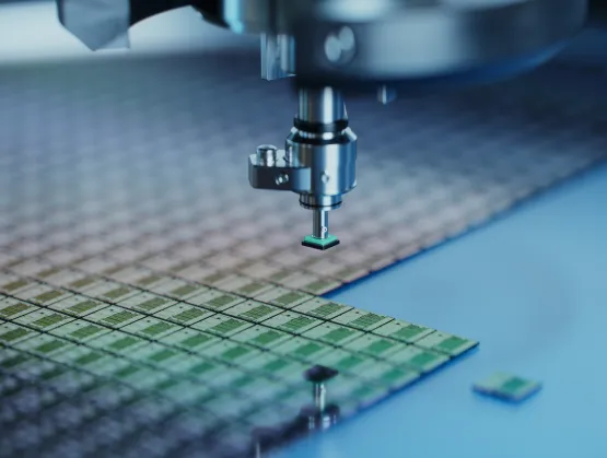
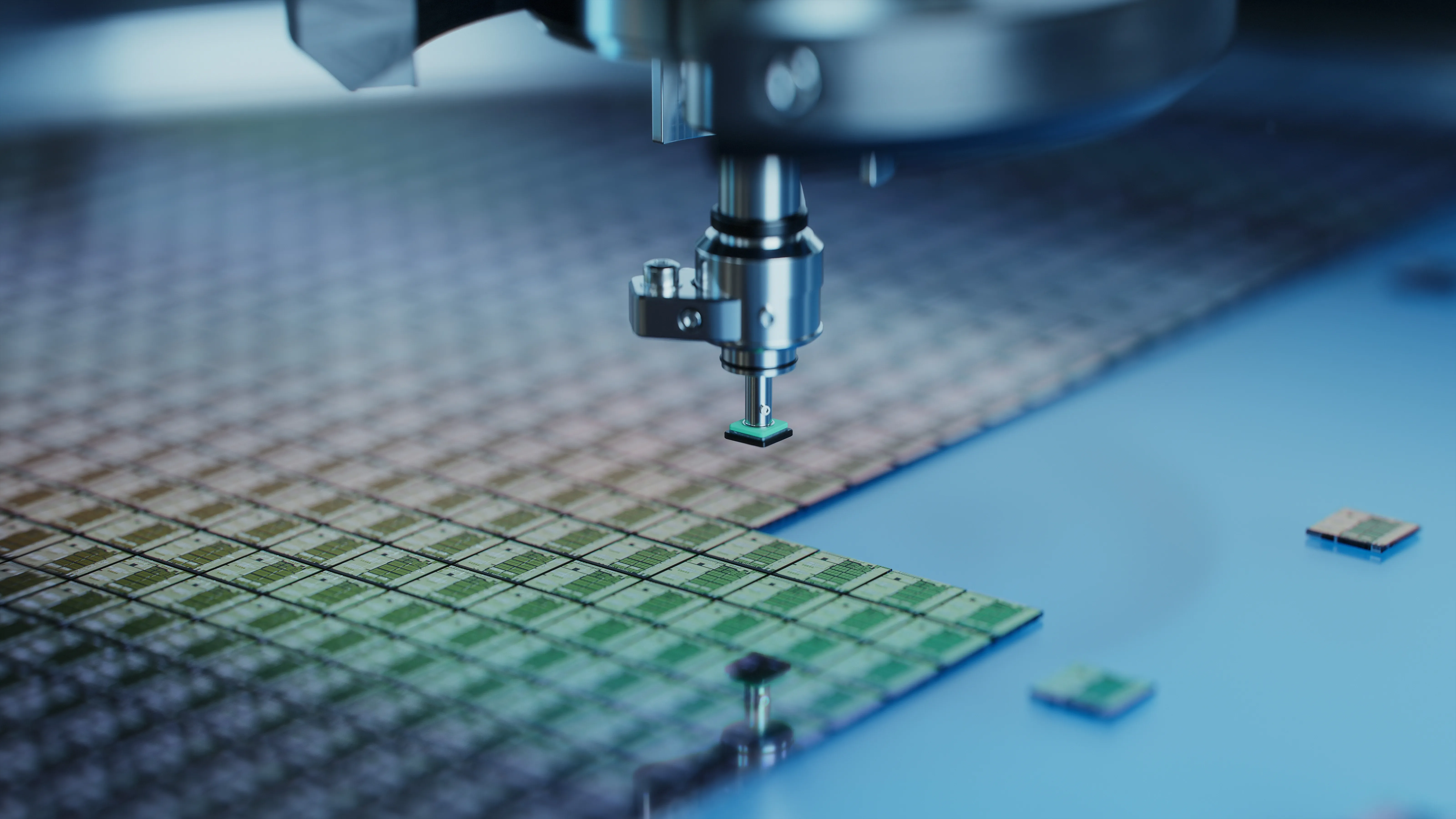
At SEMICON Europa 2025, the Executive Forum programs brought together experts from across the semiconductor value chain to address two critical challenges shaping the industry’s future in Europe: the transformation of the automotive sector and the pursuit of smarter, more competitive manufacturing.Smart Mobility in a Changing MarketKnut Krümmel, Senior Partner Automotive at Porsche Consulting, set the tone with a stark question, “Are we facing a Detroit scenario in Europe, especially in Germany?” – a reference to the decline since the 1990s of the famous “Motor City.” He pointed out that all three of Germany’s giant OEMs, Volkswagen, Mercedes-Benz and BMW, are rapidly losing market share in China in the face of a destructive price war, and have suffered large declines in reported earnings. Krümmel outlined four strategic imperatives for Europe’s auto industry: reduce complexity and increase standardization, become software-defined, design regulation that supports innovation, and build stronger partnerships across the ecosystem. He emphasized, “A new mindset is needed—people need to be hungry to win and prepared to suffer in pursuit of victory.”Knut Krümmel, Senior Partner Automotive, Porsche Consulting GmbHAndreas Aal, Head of Semiconductor Strategy at Volkswagen AG and Chair of Europe at SEMI Smart Mobility Global Automotive Advisory Council (GAAC), introduced a proactive approach to redefine the market. He shared Volkswagen’s vision for mobility-as-a-service, exemplified by its roboshuttle pilot in Hamburg. “It is very difficult for a traditional OEM to go into the full digital services world. But this is what we want to do,” said Aal.Andreas Aal, Semiconductor Strategy Volkswagen AG and Chair of Europe GAAC, VolkswagenJan-Philipp Gerhmann, Vice President of Marketing and Strategy for Automotive at NXP Semiconductors, added that the traditional value chain is being upended. The industry is shifting from a hierarchical supply chain to vertical integration, with companies like Tesla designing their own chips. Gehrmann introduced NXP’s CoreRide platform, a modular “skateboard” architecture enabling plug-and-play Advanced Driver Assistance Systems (ADAS) and infotainment features for future vehicles.Jan-Philipp Gehrmann, Vice President of Marketing Strategy, NXPA perspective on the future of semiconductors in autonomous vehicles was provided by Dieter Hoffend, Business Director for Automotive at imec: “For autonomous vehicles, you need a higher-end compute capability, which needs a transition to smaller nodes – and that is very costly. In fact, semiconductor companies will not want to commit volume to automotive customers for their most expensive leading-edge ICs. This means that a chiplet architecture will be the most cost-effective approach for vehicles, and will provide the greatest supply chain resilience. To support this, imec’s vision is of an open chiplet marketplace of heterogeneous chiplets which are interoperable.”Dieter Hoffend, Business Director Automotive Sector, imecAchieving End-to-end Manufacturing ExcellenceThe Executive Forum then shifted to a discussion of smart semiconductor manufacturing. Giovanni Notarnicola, Partner at Porsche Consulting, highlighted the untapped potential of AI in fabs. “AI requires massive amounts of data—but fabs often don’t own or control their data. And second, AI talent doesn’t typically reside in semiconductor companies,” said Notarnicola. His recommendation: “AI is not an IT issue—it’s a cross-functional technology. Isolating AI in the IT department is an old-fashioned view which will deter AI talent from joining the industry.”And Notarnicola encouraged the industry to leverage the new white paper produced by SEMI End-to-End Smart Manufacturing Group, which provides an in-depth report on the application of AI in semiconductor fabrication. Giovanni Notarnicola, Partner, Porsche ConsultingOliver Aubel, Corporate Lead for Automotive Solutions at GlobalFoundries, echoed the opportunity. “We have 1 billion sensors in a fab, but 30% of the signals are statistical noise. AI could help us make better sense of the data.”Oliver Aubel, Corporate Lead for Automotive Solutions at GlobalFoundriesA session on smart manufacturing brought to light other proven methods for improving the performance of fabs. Dr. Holland Smith, Director of Data Science at INFICON, described fab control technology that INFICON had helped STMicroelectronics to deploy. As Thomas Gimmig, Director for Industry 4.0 at STMicroelectronics, said, “Our model was a highway control room – a place where a single person controls 220km of road monitored by 400 cameras, and handles one alert every three minutes on average. This is only possible with a huge amount of automation.”Left: Thomas Gimmig, Director for Industry 4.0 at STMicroelectronics; Right: Dr. Holland Smith, Director of Data Science at INFICONAt STMicroelectronics, the new fab control room mimics this model, automating anomaly detection and problem solving. Smith described how the system will not be limited to detecting and handling anomalies which have already occurred. “There is a plan to look ahead at problems which could emerge in future, and to configure it to make proactive suggestions which will prevent anomalies from occurring in the first place,” said Smith. Jamie Potter, co-founder and CEO of Flexciton, showcased how intelligent scheduling tools based on real-time fab capacity are transforming operations. “In the modern fab decisions must be made more frequently, with more intelligence and with fewer people. And that is why fabs need to be made more autonomous,” said Potter.Jamie Potter, CEO Cofounder, Flexciton Ltd“Our tool is based on a dynamic capacity model of the fab, so WIP optimization is based on knowledge of what the fab can actually do now, rather than – as is normally the case in fabs today – on an abstract algorithm which is derived from operational results observed in the past.” Potter said. Robert Wallace, Solutions Architect at Seagate, which has deployed the Flexciton technology, confirmed the impact: “We increased throughput without increasing cycle times, and saw a 30% drop in deviations from forecast completion times.” Robert Wallace, Solutions Architect at SeagateAntoine Amade, President (EMEA) of Entegris, emphasized the importance of benchmarking to guide performance improvements: “We have a robust library of fab case studies. These benchmarks can become the foundation for best practices.” Antoine Amade, President (EMEA) of EntegrisRegulatory Burdens and Regional Challenges In a panel session, the discussion turned to the issues that European semiconductor manufacturing faces in particular. Herbert Blaschitz, Executive Vice President of Advanced Technology Facilities at Exyte, put a strong emphasis on the drag that European regulation imposes on the construction of new fabrication plants: “There is three times more paperwork to complete in Europe than in Asia.” Blaschitz made the contrast with Taiwan, “where they have standard codes of regulation specifically for a wafer fab. In Europe, we have regulations for skyscrapers, we have regulations for building family homes. But we have nothing for wafer fabs.”It could be worse for companies building all new fabs. According to Stephen Rothrock, President and CEO of ATREG, “We are affected by permits and politics most of all when trying to push through the repurposing of fabs.”From Left to Right: Mark Puttock, Sr. Director - Technology and Innovation, Entegris; Giovanni Notarnicola, Partner, Porsche Consulting; Stephen Rothrock, President/CEO, ATREG; Jean-René Lèquepeys, Deputy Director and Chief Technology Officer, CEA-Leti; Herbert Blaschitz, Executive VP of Advanced Technology Facilities, Exyte; Oliver Aubel, Corporate Lead Automotive Solutions, GlobalFoundriesSustainable Manufacturing Practices: A Source of Competitive Advantage?The forum ended with a debate on the value of and problems with Europe’s commitment to sustainability. As Mark Puttock, Senior Director for Technology and Innovation at Entegris, acknowledged concerns that sustainability practices could raise costs and reduce process efficiency. But Jean-René Lèquepeys, Deputy Director and Chief Technology Officer at CEA-Leti, countered: “sustainability can be a competitive advantage. For instance, the industry is under pressure to eliminate PFAS from its processes. CEA-Leti is working on this problem, and the whole world is looking for a solution.”The event concluded with a moment of celebration: Ilya Zabelinsky, Co-founder of the International Subfab Research Labs (ISRL), won a diamond prize sponsored by Nanores Lab,Left: Jakub GawczyńskiJakub Gawczyński, Head of Nanores Lab; Right: Ilya Zabelinsky, Co-founder of the International Subfab Research Labs (ISRL)On behalf of SEMI, we extend our sincere gratitude to the speakers, sponsors, and participants who contributed their expertise and vision to the programs at SEMICON Europa 2025.SEMI ContactAna Bernardo, Senior Manager of Technology Programs SalesEmail: [email protected]
Read More
The GENESIS EU project is reshaping how Europe thinks about semiconductor manufacturing. Its goal is simple but ambitious: reduce usage of harmful chemicals from chip production, cut emissions and waste, and make the industry more circular and resilient.Launched on 1 May 2025, GENESIS – GENerate in Europe a Sustainable Industry for Semiconductor – is a research and innovation project co-funded by the European Union through Chips JU and its participating member states. In addition, Swiss partners are supported by the Swiss State Secretariat for Education, Research and Innovation (SERI).Coordinated by CEA-Leti in Grenoble, GENESIS brings together 58 partners from across the semiconductor value chain: materials and chemistry suppliers, equipment manufacturers, semiconductor fabs, research and technology organisations (RTOs), universities, small and medium-sized enterprises (SMEs), recycling specialists and communication experts. Together, they are working to build a resilient, circular and environmentally responsible microelectronics sector aligned with the European Green Deal and the European Chips Act.Mission and VisionGENESIS exists to future-proof the European semiconductor industry. The project focuses on:Eliminating or replacing per- and polyfluoroalkyl substances (PFAS) and other hazardous substances used in manufacturing processes;Reducing waste and greenhouse gas emissions throughout the production chain;Securing access to critical materials through smarter use, reuse and circular strategies;Deploying advanced monitoring and sensing solutions for gas and liquid environments in fabs.Six Work Packages, One Integrated ApproachTo reach its objectives, GENESIS is structured into six work packages.Work Package 1 – Management, Specifications, and MethodsLead: CEA-LetiWP1 keeps the project on track. It manages the technical, administrative and financial coordination of GENESIS and defines common specifications and methodologies. This includes setting technical recommendations and carrying out environmental impact assessments so that shared targets and consistent methods guide all subsequent work.Work Package 2 – Process, Monitoring Sensing Hardware and SolutionLead: CSEMWP2 develops real-time monitoring technologies capable of detecting and quantifying emissions from process gases such as NF₃, CF₄ or SF₆. By improving transparency and enabling process feedback, GENESIS contributes to the transition toward low-emission semiconductor fabs aligned with EU climate goals.Work Package 3 – Environmentally Friendly Materials AlternativesLead: imecWith global PFAS restrictions tightening, the semiconductor sector urgently needs high-performance, safe alternatives. GENESIS in WP3, is designing and qualifying materials for key manufacturing steps including lithography, etching, cleaning, deposition, and packaging, that reduce industry dependence on PFAS and higher GWP gases while ensuring compatibility with industry performance requirements.Work Package 4 – Minimisation of Waste and EmissionsLead: FraunhoferWP4 addresses the complexity of semiconductor waste streams and explores innovations to enhance abatement efficiency. GENESIS develops recycling, recovery, and closed-loop solutions for gases, slurries, and solvents, with the aim of significantly reducing waste across fabs.Work Package 5 – Materials Scarcity Impact MitigationLead: Università degli Studi di Roma Tor VergataEurope’s dependence on critical raw materials—including gallium, indium, and rare earth elements—represents both an environmental and strategic challenge. GENESIS in WP5 focuses on reducing CRM usage through process innovation and strengthening circularity to enhance supply chain resilience.Work Package 6 – Regulations, Dissemination, Communication and ExploitationLead: SEMI EuropeWP 6 is dedicated to ensuring that GENESIS creates meaningful and lasting impact beyond its technical achievements. It integrates regulatory monitoring, dissemination, communication, and exploitation activities to connect the project’s innovations with industry needs, European policy developments, and wider society. WP6 is coordinated by SEMI Europe, supported by expert partners across the consortium, and serves as the bridge between GENESIS’s scientific work and its real-world influence.Long-term strategyGENESIS is built with one goal in mind: making sure the work happening inside the project translates into real change across Europe’s semiconductor ecosystem. To support this, the project focuses on four key impact areas that help move ideas from research into industry, policy and long-term community engagement.Helping Industry Put Results to WorkA core part of GENESIS is understanding how each partner can use the project’s results in their own environment. Whether it’s new materials, smarter monitoring solutions or better waste-reduction approaches, partners define clear pathways for adoption so GENESIS innovations can move naturally into real industrial use.Staying Connected to Europe’s Policy AgendaSustainability and chemical regulations in Europe are evolving fast, and GENESIS stays close to these developments. The project brings technical insights to discussions around the Green Deal, PFAS regulation, and critical raw materials. This makes sure GENESIS is not only aligned with policy trends, but also contributes to shaping them.Making Knowledge Accessible and Future-FocusedOpen access is an essential part of GENESIS. The project shares its research outputs publicly and supports the creation of educational material for universities and training programmes. This helps the next generation of engineers and specialists build on GENESIS knowledge and carry it forward.Keeping GENESIS Visible and RelevantGENESIS maintains a strong presence across events, conferences, publications and expert discussions. This ongoing engagement ensures that project results remain visible, understood and connected to wider conversations on sustainable semiconductor manufacturing—helping extend the project’s influence well beyond its duration.Towards a Sustainable Semiconductor FutureGENESIS shows that high-performance chips and environmental responsibility can coexist. By uniting materials science, process engineering, monitoring technologies, environmental assessment and policy insight, GENESIS is helping define what responsible, future-ready semiconductor manufacturing will look like tomorrow.Jatin Mendiratta, Communications CoordinatorSEMI Europe Phone: +49 160 402 8899Email: [email protected]
Read More
In an era where performance and efficiency are essential, heterogeneous integration is rapidly becoming a foundational technology. The webinar “Heterogeneous Integration in Action: Powering the Next Era of Connectivity” featuring speakers from the HiCONNECTS project dives deep into the advances, challenges, and ecosystem-building necessary to bring next-generation integrated systems to life across Europe and beyond.HiCONNECTS (Heterogeneous Integration for Connectivity and Sustainability) brings together more than 60 partners across Europe under the Chips JU to explore how packaging, materials, architectures and software can be co-designed for industrial uptake.A Bold Ambition: Why This MattersConnectivity is the lifeblood of our digital age. From smart mobility and data centers to consumer electronics and factory automation, demands on performance, energy efficiency, miniaturization and flexibility keep growing.Heterogeneous integration offers a path to meet those demands by enabling dissimilar technologies, for example chips, sensors, RF, photonics, advanced packaging and AI accelerators to work together more seamlessly than ever before.Set against the backdrop of Europe’s broader ambitions under the EU Chips Act to strengthen its semiconductor ecosystem and technological leadership, projects like HiCONNECTS demonstrate how coordinated R D can translate into industrially relevant demonstrators and use cases.Key Themes from the WebinarBelow are some of the most compelling takeaways from the session:From Components to SystemsAcross all talks, one message was clear: heterogeneous integration is no longer just about better individual devices, it’s about system-level co-design.Speakers showed this in very concrete ways:In power device manufacturing, improving yield, process control and data correlation across the wafer line directly improves the reliability of integrated systems.In smart logistics and manufacturing, autonomous mobile robots combine LiDAR, cameras, 5G, on-board compute and collaborative AI to operate safely on factory floors.In life-science imaging, cryo-electron microscopes, AI-assisted screening and high-performance computing are tied together into a single workflow.In connected and autonomous mobility, radar, V2X modems, explainable AI software and human–machine interfaces form one integrated chain.You can no longer treat sensing, connectivity, compute and packaging in isolation – the value lies in how they are composed into complete systems.Ecosystem Consortium DynamicsTo realize heterogeneous integration, no single entity can go it alone. The webinar highlighted how large consortia such as HiCONNECTS bringing in universities, research institutes, packaging houses, system vendors, and tool suppliers are key. A strong theme: modularity and interfaces must be agreed upon early to allow parallel work across partners.Why Europe’s Timing is CriticalHiCONNECTS sits within a broader European push to strengthen the continent’s semiconductor capabilities and reduce systemic vulnerabilities in critical value chains. Europe already hosts strong players in photonics, packaging, system integration, robotics, automotive and research.What the webinar underscored is that coordination and shared infrastructure are now decisive:aligning manufacturing know-how with AI and data analytics,connecting application-driven demonstrators with underlying technology platforms, andensuring results can be replicated and scaled beyond a single lab or pilot line.Final ThoughtsThe “Heterogeneous Integration in Action” webinar was a timely, forward-looking snapshot of how Europe’s microelectronics ecosystem is moving from component-level innovation to system-level co-design, grounded in real industrial use cases.The journey is far from complete, but the payoff is clear: higher-performance systems, new classes of products in mobility, health and manufacturing, and a stronger, more resilient European position in semiconductors.Kartikey Srivastava, Manager, EU ProjectsSEMI Europe Phone: +49 151 1436 6324Email: [email protected]
Read More