

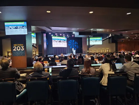
SEMI’s annual Surface Preparation & Cleaning Conference (SPCC) brought industry experts to Chandler, Arizona, to address the biggest challenges affecting this area of the semiconductor industry. As the premier technical forum dedicated to advancing surface preparation, cleaning technologies, and wet processes, the conference featured dozens of speakers who shared insights on the current market, emphasizing key themes like advanced packaging, power delivery, advanced DRAM, sustainability, and more.
Ahead of this year’s conference, SEMI and Global Net Corp. (GNC) developed a new report, Glass Core Substrate Market and Development Trends, examining manufacturing challenges, supply chain structure, and market outlooks through 2040. This resource helps organizations evaluate the glass core substrate landscape before committing to production. A sample of the report is available for complimentary download.
High-Level Updates and SEMI Insights
Joe Stockunas, president of SEMI Americas, kicked off SPCC 2026 by announcing that the industry is entering its biggest era yet, on pace to reach $1 trillion in annual revenue in 2026 – 4 years ahead of prior forecast. The semiconductor industry has become the third most valuable global industry with top companies' market capitalization surging over the past decade. By 2030, industry analysts expect annual revenue to soar to $1.9 trillion, driven largely by demand for AI infrastructure, with logic and micro capacity also expected to nearly double. However, Stockunas also noted headwinds including geopolitical tensions and a growing talent shortage.
Duncan Meldrum from Hilltop Economics offered a cautionary macroeconomic view, warning that AI growth is now concentrated among a handful of hyperscalers and leading-edge chipmakers, creating concentration risk. Geopolitically driven inflation is squeezing consumers, while supply chain disruptions are impacting critical materials like sulfuric acid, helium, and tungsten. Meldrum also highlighted concentration risk in production, with a few ODMs and manufacturers dominating the AI server market.
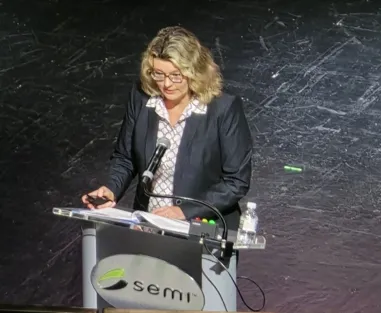 SEMI analyst Inna Skvortsova provided materials market updates, emphasizing that advanced devices are driving materials intensity per wafer. Lithography, wet chemicals, and CMP are already seeing double-digit growth, led by increasing number of processing steps, rising count of EUV layers, and tightening CMP process windows at advanced nodes. Deposition materials were noted as another fast-growing segment that is forecast to grow at a 13.5% CAGR through 2030, driven by molybdenum adoption and backside power networks. Furthermore, introduction of new materials, including Ruthenium and Tungsten Carbon Nitrite (WCN) hardmasks, brings new opportunities and challenges with regards to wet processes.
On memory, Skvortsova confirmed that AI pull has made memory a compute-stack bottleneck, driving capital toward leading-edge logic and HBM. Logic and micro capacity nearly doubles by 2030, but growth is highly concentrated in advanced nodes (≤7nm) pressuring non-AI segments.
Skvortsova also highlighted a supply chain shift from globalization to localized production networks, with China emerging as a significant player in areas like bulk wet chemicals, gases, and deposition materials. While alternative sources are emerging, supplier re-qualification may result in higher material costs.
Theme 1 - Hybrid Bonding & Flux
SPCC 2026 highlighted cleaning innovations for hybrid bonding, a core technology enabling AI scaling and glass core substrates. Srini Raghavan (ProSys) presented a paper based on the collaborative work between Intel and ProSys in the area of megasonic removal of flux from narrow gaps in advanced packaging structures. His team found that application of 10 msec pulses of 925 kHz sound wave at 90% duty cycle was very effective in flux removal in a semi-aqueous formulation Acoustic streaming rather than cavitation appears to be the primary cleaning mechanism under the test conditions.
Koji Nakata (Kurita Industries) tackled particle contamination, copper corrosion, and chemical consumption in 3D stacking. His solutions include:
- Functional water + megasonic cleaning for higher particle removal than SC-1.
- Alkaline water rinsing to reduce copper pad recessing vs. DI water.
- Functional water to lower chemical consumption, cost, and environmental impact.
Theme 2 – Wet Etch, Gate-All-Around, & Selectivity
Two presentations highlighted next-gen logic wet etch challenges. IBM's Alma Vela Ramirez showed that an oxide-selective wet chemistry reduced buried void defects by over 20× during dummy gate polysilicon removal in GAA nanosheet flows. From her findings, chemistry 1 showed higher defectivity, while chemistry 2, selective to gate oxide and compatible with spacers, drastically reduced void formation by preserving the bottom oxide layer.
Mitsubishi Chemical Corporation’s Tomoki Nara demonstrated a Si/SiGe selective etchant achieving a record 750:1 selectivity, critical for protecting thin SiGe layers during Si thinning in backside power delivery networks (BSPDN). His new alkaline wet etchant and single-wafer spin process address conventional etchants' inability to stop cleanly on SiGe, significantly expanding the process window during Si thinning and reducing the risk of SiGe damage.
Theme 3 – Scaling DRAM to Advanced Nodes
Micron presented two DRAM manufacturing breakthroughs. Shihui (Adara) Yang introduced a dilute sulfuric peroxide clean achieving 3.59× BCF:TCF (bottom container fill and top container fill) selectivity—solving uniformity issues where conventional fluorine-based chemistries etch both layers at similar rates, causing container shorts and yield loss at advanced nodes.
Hiroki Uoyama introduced a wafer backside polishing brush incorporating diamond or silicon carbide, achieving over 90% defect height reduction with no wafer thickness loss. This physical cleaning approach improves focus control, alignment accuracy, and overall yield — critical as lithography margins narrow dramatically at smaller nodes.
Theme 4 – Sustainable Materials & Stripping Solutions
Sustainability was another core focus at SPCC 2026, with three distinct approaches taking center stage — each addressing a different facet of environmental impact in the fab.
- PFAS are among the major pollutants in semiconductor manufacturing waste streams, whose separation and destruction are challenging. As demonstrated by imec’s Sina Kaabipour, representing the collaborative research work between imec, Purdue University, and Enspired Solutions, UV destruction can achieve more than 99% PFAS destruction efficiency for simulated semiconductor manufacturing waste, showcasing great potential for scale-up and direct mineralization from liquid fab waste effluents.
- Diane Bijou from Technic launched TechniStrip® Micro 680, an NMP-free stripper with sub-2-minute stripping time, better loading capacity, extended bath life, and lower cost per wafer than NMP/amine-based strippers.
- Chihiro Kobata of JSR unveiled a water-rich stripper removing both photoresist and spin-on glass without NMP, DMSO, and TMAH, at lower temperatures (40–60°C), with ECO conscious, high performance, and high material compatibility and fab-part compatibility.
Connect With SEMI
SEMI would like to thank all speakers, sponsors, and attendees for the success of SPCC 2026. Download a preview of SEMI and GNC’s new report, Glass Core Substrate Market and Development Trends, and stay connected with SEMI on LinkedIn and X.
Clark Tseng is Senior Director of Market Intelligence at SEMI.


