downloadGroupGroupnoun_press release_995423_000000 copyGroupnoun_Feed_96767_000000Group 19noun_pictures_1817522_000000Member company iconResource item iconStore item iconGroup 19Group 19noun_Photo_2085192_000000 Copynoun_presentation_2096081_000000Group 19Group Copy 7noun_webinar_692730_000000Path
Skip to main content
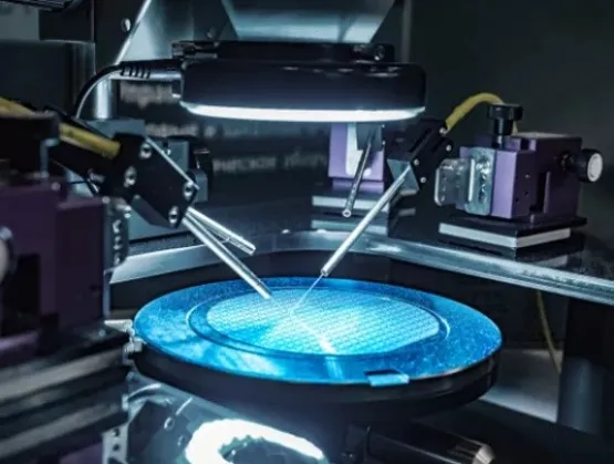
Artificial intelligence (AI) and high-performance computing (HPC) are driving unprecedented demand for data movement. As bandwidth requirements climb and conventional electrical interconnects encounter limitations in power consumption, latency and reach, silicon photonics, near-packaged optics (NPO), and co-packaged optics (CPO) are becoming increasingly important technologies for next-generation data centers.Much of the industry’s attention has focused on photonic device innovation. But demonstrating a high-performance photonic integrated circuit (PIC) is only part of the challenge. Turning these devices into products that can be manufactured reliably and economically at high volume requires a test infrastructure that can keep pace.This represents a significant shift. Semiconductor manufacturing has benefited from decades of refinement in automated electrical test. Silicon photonics adds an optical dimension that brings new requirements for fiber alignment, coupling efficiency, polarization management, and optical instrumentation—while still requiring conventional electrical characterization.As silicon photonics moves from development environments toward high-volume production, test becomes more than a quality gate. It is an integral part of the manufacturing strategy.An HVM-ready test solution requires a full complement of supporting hardware and software.Bringing precision optical alignment to productionOne of the most fundamental challenges is establishing a reliable optical connection to the device under test. Unlike electrical probing, where physical contact provides a relatively straightforward interface, optical testing depends on precisely coupling light into and out of very small structures.That coupling must be repeatable from device to device and wafer to wafer. Even small variations in fiber position or angle can affect insertion loss and measured optical performance, potentially making it difficult to distinguish actual device variation from variation introduced by the test setup.For this reason, high-volume testing requires automated alignment capabilities that can quickly locate the optical interface and optimize coupling. This can involve visual or image-based positioning to bring a fiber array unit close to the grating couplers, followed by area scans and gradient-search techniques to identify the optimal position via feedback loops – a technique typically referred to as “active alignment.” The process may also require optimization across six degrees of freedom—X, Y, and Z positioning plus three rotational axes—to maximize coupling efficiency and minimize channel-to-channel variation.The problem becomes more complex as optical interfaces add channels. Alignment must not simply maximize one channel's performance; it must produce consistent coupling across multiple channels. Rotational alignment, for example, can influence how evenly an optical beam overlaps multiple grating couplers. Other angular adjustments can affect both insertion loss and center wavelength.Polarization presents another variable. Because photonic structures can respond differently depending on the polarization state of incoming light, polarization must be characterized and controlled as part of a repeatable production methodology. Together, these requirements make alignment an active measurement and optimization process rather than a simple mechanical positioning step. The manufacturing challenge is to automate these functions without allowing alignment time to become a throughput bottleneck.Combining electrical and optical test without sacrificing throughputAlignment is only one part of the equation. A PIC may incorporate photodetectors, modulators, and other components requiring combinations of optical and electrical measurements. Typical characterization can include insertion loss, channel-to-channel uniformity, optical attenuation, photodetector responsivity, and wavelength-dependent behavior.Performing these measurements sequentially can add substantial test time. A more scalable approach is to integrate electrical and optical capabilities so that operations can occur concurrently wherever possible. For example, electrical alignment can occur before optical alignment, while continuity and other electrical tests may run during automated optical probe alignment rather than waiting for that process to finish. This type of parallelism becomes increasingly important as device complexity and test coverage grow.The same principle applies to optical instrumentation. Rather than treating each instrument as an isolated resource, high-volume environments benefit from integrated control of lasers, power meters, and other optical equipment, enabling parallel operation of multiple instruments or channels. Automated calibration and compensation are also important for maintaining measurement consistency as the test cell becomes more complex. Advantest’s development work in this area supports multiple optical instruments and parallel power-meter operation within a common test environment.The broader objective is familiar from semiconductor test: maximize useful test coverage while minimizing test cost. What changes with silicon photonics is the number of physical and measurement domains that must be coordinated to achieve it.Collaboration will be essential to ecosystem scalingNo single supplier controls all of the elements required for high-volume PIC test. The complete solution can span automated test equipment, wafer probing, optical positioning, fiber interfaces, optical instrumentation, device design, and manufacturing processes.That makes ecosystem collaboration particularly important. Test equipment providers need to work with probe and positioning specialists, photonic device developers, foundries, and manufacturers so the interfaces among these technologies function as an integrated production system rather than individual laboratory instruments.As an example, Advantest has collaborated closely with FormFactor to develop a wafer-level photonics test environment that combines electrical test instrumentation with wafer handling, optical instruments, and automated fiber alignment capabilities. The significance lies less in individual components than in the integration required to create a repeatable manufacturing workflow.As silicon photonics, NPO and CPO move toward broader adoption, these collaborative efforts will become increasingly important. The industry must develop practical test methodologies that accommodate evolving device architectures while delivering the repeatability, throughput, and economics expected of semiconductor manufacturing.Numerous photonics developments on the horizon will require broad industry effort to bring to fruition.The transition from promising photonic technology to high-volume commercial products will depend on more than advances in the devices themselves. Test must evolve alongside them. By treating optical alignment, electrical and optical measurement, automation, and ecosystem interoperability as parts of a single manufacturing challenge, the industry can build the infrastructure needed to bring silicon photonics fully into the era of high-volume production. About the AuthorDr. Clemens Leichtle is Senior Director and V93000 Photonic Business Lead for Advantest Corp. He has more than 25 years of experience in the semiconductor industry, with companies including Siemens, Agilent and Verigy, specializing in testing and developing respective application solutions for emerging technologies. For more than 15 years, he has been leading the V93000 Center of Expertise at Advantest; more recently, he co-led test solution development for silicon photonics and co-packaged optics targeting data center applications. Dr. Leichtle holds a Ph.D. in physics from the University of Ulm, Germany.
Read More
As Taiwan’s semiconductor, high-tech, artificial intelligence, and export-oriented sectors continue to grow, renewable energy has evolved from an ESG option into an increasingly important consideration for supply-chain competitiveness, decarbonization commitments, and long-term business planning.Surplus Renewable Energy Does Not Mean “Too Much Renewable Energy”One distinction is essential when discussing Surplus Renewable Energy (Surplus RE): its existence does not mean that Taiwan has too much renewable energy, nor does it indicate system-wide market oversupply.Recent RE100 observations continue to identify high costs and limited supply as key barriers to corporate renewable energy procurement, indicating that corporate demand remains clear while both supply and procurement pathways still have room to expand. Data presented by Taiwan’s Executive Yuan Office of Energy and Carbon Reduction at the September 4 Energy Collaborative Forum likewise showed that renewable electricity generation increased from 4.8% of Taiwan’s power mix in 2016 to approximately 13.1% in 2025, underscoring the growing role of renewables in the electricity system.Two distinct phenomena are at work: Taiwan’s overall market still needs more renewable energy, while individual companies may experience unmatched electricity as long-term procurement expands. The first concerns whether Taiwan’s renewable energy supply is sufficient to meet corporate demand. The second arises when contracted generation profiles and procurement volumes do not align with a company’s electricity load within the applicable time periods.In this article, Surplus RE refers to renewable electricity that has already been procured but cannot be wheeled as originally intended because generation and consumption do not align within the applicable time parameters. Its occurrence and scale vary according to corporate load profiles, procurement volumes, energy mix, and project commercial-operation schedules. It does not mean that all companies currently face a Surplus RE issue. Rather, it reflects a market-matching and institutional-design challenge that becomes increasingly relevant as corporate renewable energy procurement expands—not an oversupply of renewable energy across Taiwan.Taiwan has also recently made concrete institutional progress in corporate renewable energy matching and Surplus RE treatment, including greater flexibility in wheeling allocation and continued policy work on the treatment of unmatched electricity and its associated environmental attributes. These developments are more than technical refinements: they increasingly respond to practical considerations in long-term corporate procurement, project investment and financing, and the continued development of Taiwan’s renewable energy market.Rigorous Matching and Certificate Rules Are an Important Foundation of Taiwan’s Renewable Energy MarketTaiwan applies a relatively rigorous framework to corporate renewable energy wheeling and recognition. Under the current arrangement, generation and consumption are matched primarily using 15-minute metering data. Once renewable electricity is successfully wheeled, Taiwan Renewable Energy Certificates (T-RECs) are issued based on the actual wheeled volume. This closely links certificate issuance to electricity delivery, strengthening the traceability of environmental attributes, the connection between generation and consumption, and the credibility of corporate renewable energy claims.This differs from some international markets, where certificates are generally issued against eligible renewable electricity generation and may subsequently be traded separately from the physical electricity. In the U.S., Renewable Energy Certificates (RECs) are created when renewable electricity is generated and delivered to the grid, while in the U.K., one Renewable Energy Guarantee of Origin (REGO) is issued for each 1 MWh of eligible generation. Taiwan, by comparison, more directly links certificate eligibility to actual wheeling outcomes. Time matching therefore affects both whether electricity can be wheeled as intended and whether the corresponding environmental attributes can be obtained and recognized.Where contracted renewable electricity cannot be matched as intended because of differences between generation and load, the unmatched volume does not, under the existing treatment, receive the corresponding certificates in the same manner as successfully wheeled electricity. The matching and certificate framework itself does not cause Surplus RE; rather, it turns underlying timing differences between generation and consumption into practical market issues involving certificate access, cost allocation, and commercial arrangements.Recent RE100 data provide another useful perspective. While the share of recognized renewable electricity among RE100 members in Taiwan still has room to grow, the gap between reported and ultimately recognized renewable electricity remains relatively limited. This suggests that a substantial share of reported corporate renewable energy procurement meets the applicable recognition requirements.The next stage for Taiwan is therefore not to lower existing standards for recognition or environmental integrity, but to increase flexibility in how companies allocate and use renewable energy while preserving credibility and traceability — allowing market efficiency and environmental integrity to advance together.The Nature of Renewable Electricity Makes Perfect Matching DifficultSurplus RE is closely related to both renewable electricity generation characteristics and corporate consumption patterns. Solar has a distinct daytime generation profile, wind output varies with wind conditions, and hydropower has its own supply characteristics. At the same time, different companies, facilities, and manufacturing processes have different electricity-load profiles.Companies can combine wind, solar, hydropower, and projects across different locations to improve the match between renewable electricity supply and their own load. Even so, generation and consumption profiles are unlikely to align perfectly at all times. Where contracted renewable electricity exceeds the company’s matchable load during a particular period, part of that electricity may be unable to complete the originally intended wheeling arrangement and become Surplus RE.The actual scale of Surplus RE depends on the volume of renewable energy procurement relative to the company’s load, its energy mix, project generation profiles, and project commercial-operation schedules. Where current procurement volumes can still be fully absorbed by the company’s own load, Surplus RE may remain limited. As long-term procurement volumes increase or medium- and large-scale renewable energy projects progressively reach commercial operation, time-matching issues may become more material.Surplus RE is therefore not a fixed percentage faced by all companies at the same time. It is a market-design issue that becomes increasingly relevant as corporate procurement and new renewable energy supply expand.When Take-or-Pay Meets Time MatchingFor corporate buyers, Surplus RE is more than a technical settlement issue. It is closely tied to the commercial structure of corporate power purchase agreements and the financing of renewable energy projects. Medium- and large-scale CPPAs are typically long-term contracts and may include take-or-pay provisions. These commitments improve revenue predictability for developers and are an important factor in financial institutions’ assessment of project cash flows and bankability.Under a take-or-pay structure, however, a company may still be contractually required to pay even if part of the renewable electricity cannot be wheeled as intended because of time-matching constraints. Under the original framework, the unmatched portion was also unable to receive the same certificate and environmental-attribute recognition as successfully wheeled electricity. As procurement volumes increase, corporate buyers therefore need to consider not only how much renewable energy they contract, but also how much electricity can actually be wheeled and utilized, and how any unmatched portion will be treated.To avoid conflating statutory renewable energy obligations with voluntary corporate procurement, the following simplified scenario illustrates the potential commercial scale of unmatched electricity under a long-term CPPA. The assumptions are illustrative only and do not represent average procurement volumes, an average Surplus RE ratio, or a forecast for the Taiwan market.Assume that a company enters into a CPPA for 50 GWh per year to support its renewable energy and supply-chain objectives. At an illustrative energy price of NT$6 per kWh, the annual notional purchase value would be approximately NT$300 million. If, after load management, portfolio diversification, and cross-facility allocation, 20% remains unmatched, approximately 10 GWh per year would fail to complete the intended wheeling arrangement, corresponding to a notional purchase value of approximately NT$60 million per year.This article uses 25 years as an illustrative contract term, reflecting the midpoint of approximately 20- to 30-year CPPA terms already seen in Taiwan’s large-scale offshore wind market. This does not imply that all CPPAs use the same tenor. Assuming price, generation volume, and the unmatched share remain constant, and excluding discounting, price adjustments, and other contractual terms, the cumulative notional value associated with the unmatched portion would be approximately NT$1.5 billion over 25 years.Table: Illustrative Long-Term Corporate CPPA Scenario:ItemAssumption / FormulaResultAnnual CPPA procurement volumeIllustrative assumption50 GWh/yearCPPA energy purchase priceIllustrative assumptionNT$6/kWhAnnual notional contracted purchase value50,000,000 kWh × NT$6/kWhApprox. NT$300 million/yearIllustrative unmatched shareIllustrative assumption20%Annual unmatched electricity volume50 GWh × 20%10 GWh/yearNotional value associated with unmatched volume10,000,000 kWh × NT$6/kWhApprox. NT$60 million/yearIllustrative CPPA termMidpoint of 20–30 year long-term offtake arrangements25 yearsCumulative notional value of unmatched portionNT$60 million × 25 yearsApprox. NT$1.5 billionNote: The 20% unmatched share is an illustrative assumption informed by scenarios reflected in industry discussions. It does not represent the average Surplus RE ratio among Taiwan companies or a future market forecast. The 25-year term is based on the midpoint of approximately 20- to 30-year long-term CPPAs already seen in Taiwan’s large-scale offshore wind market and does not represent a standard market tenor. Actual outcomes will vary according to corporate load profiles, procurement volumes, energy mix, project generation characteristics, contractual terms, and commercial-operation timing. NT$6 per kWh is likewise an illustrative energy purchase price and does not represent the full cost of corporate renewable energy procurement.This calculation should not be read as treating unmatched electricity as a direct “market loss.” Its purpose is to show how Surplus RE treatment can affect long-term procurement decisions. Where treatment mechanisms, environmental attributes, and related costs lack sufficient predictability, companies may reflect those risks in procurement volumes, pricing, or contractual terms.These decisions can in turn affect developers’ offtake arrangements and revenue predictability, with implications for project investment and financing. The significance of Surplus RE therefore lies not only in reducing unmatched volumes, but also in improving predictability for long-term procurement and financing, supporting continued growth in corporate renewable energy procurement and new supply.Public-Private Collaboration Is Gradually Improving Market DesignSurplus RE intersects with corporate procurement contracts, renewable energy certificates, project finance, transmission and distribution costs, and power-system operations. It is therefore a cross-institutional, multi-stakeholder market-design issue that cannot be addressed by any single mechanism or participant.The public-private collaboration approach recently articulated by Taiwan’s Executive Yuan Office of Energy and Carbon Reduction is consistent with this need. Relevant government agencies, Taiwan Power Company, and industry participants have held multiple rounds of discussion on flexible allocation, Surplus RE certificates, cross-time treatment of unmatched electricity, and tariffs, bringing policy objectives, corporate needs, commercial conditions, and power-system constraints into a common framework.The SEMI Energy Collaborative has also contributed through member input and policy dialogue, bringing corporate procurement practices, project commercial conditions, and market experience into policy discussions. This helps stakeholders examine practical issues together and identify arrangements that balance market efficiency, investment viability, environmental integrity, and system stability.Monthly Matching Within the Same Time-of-Use Period Is an Important StepOn September 3, 2026, Taiwan Power Company revised the Flexible Allocation Pilot Program for the Renewable Energy Market and its related operating rules. Under the existing pilot framework, the revision introduced monthly matching by time-of-use period and extended the pilot through September 30, 2028. This represents a further step in improving matching and allocation flexibility in Taiwan’s corporate renewable energy market. The revised mechanism continues to use the original 15-minute metering data as its underlying basis, aggregating generation and consumption into four time-of-use periods—peak, semi-peak, off-peak, and Saturday semi-peak—before conducting wheeling-volume matching and flexible allocation within the same month and the same time-of-use period.Table: Key Adjustments to the Flexible Allocation Mechanism for Renewable EnergyAspectPrevious FrameworkDirection After the AdjustmentUnderlying metering data15-minute generation and consumption dataStill based on 15-minute dataMatching approachMatching based on the existing time-based rulesMonthly matching within the same month and the same time-of-use periodTime-of-use periods—Peak, semi-peak, off-peak, and Saturday semi-peakAllocation modelsExisting wheeling arrangementSingle legal-entity allocation; electricity retailer allocationMain objectiveMaintain traceability and recognition qualityImprove matching and allocation flexibility while preserving traceabilityPilot periodExisting pilot frameworkExtended through September 30, 2028Note: The adjustment does not eliminate 15-minute metering. Rather, it builds on the existing metering basis by introducing monthly matching and flexible allocation within the same time-of-use period.The program retains two allocation models: “single legal-entity allocation” and “electricity retailer allocation.” This gives companies greater flexibility to allocate renewable electricity across different facilities, electricity account numbers, and load profiles, while allowing electricity retailers to play a role in electricity-volume aggregation and allocation.The core value of the mechanism lies in improving the matching and use of existing renewable electricity while preserving traceability. The longer pilot period also gives the market more time to build operating experience, validate practical needs, and inform further refinement.The Next Step for Surplus RE Goes Beyond “Eliminating Surplus”Monthly matching within the same time-of-use period can improve flexibility in matching generation and consumption. Even after flexible allocation, however, differences between generation and consumption profiles may remain across time periods. The next question therefore becomes how unmatched electricity should be treated and how its associated environmental attributes can be preserved, valued, and effectively used.There has also been concrete progress on the certificate framework. In April 2026, Taiwan’s Bureau of Standards, Metrology and Inspection (BSMI) proposed draft amendments to the Regulations Governing the Implementation of Renewable Energy Certificates. Under the proposal, renewable energy generators that have not entered into a surplus-electricity purchase and sale agreement with Taiwan Power Company could still obtain renewable energy certificates for Surplus RE, while certificates that have not been used or claimed could be transferred to other recipients.Subsequent policy discussions have also moved toward treating physical electricity and environmental attributes separately. Under the approach being examined, physical electricity that does not complete its intended wheeling arrangement would be handled through the power system, while corresponding certificate issuance based on actual unmatched volumes remains under consideration, with certificate ownership determined by contractual arrangements. The core concept is to separate the treatment of physical electricity from the preservation of environmental attributes, so that failure to complete time matching does not necessarily mean losing the associated environmental value.This does not weaken the traceability established under the existing wheeling and certificate framework. Rather, policy discussions are examining how environmental attributes associated with unmatched electricity can be treated appropriately while keeping the status of different electricity volumes clearly distinguishable. Note: The accompanying illustration reflects the current direction of policy discussion. It does not indicate that all rules governing the issuance, transfer, or compliance use of Surplus RE certificates have been finalized.Even if a future framework allows corresponding certificates to be issued for Surplus RE, two issues will still require clarification. The first is market value. Under take-or-pay contracts, corporate payment obligations generally do not change with the final matching outcome. If the unmatched portion primarily retains its environmental attributes, its cost and value structure may differ from that of a conventional certificate transaction, while the time value of electricity and the value of environmental attributes will still need to be clarified through market practice.The second is regulatory use. How such certificates should be identified, and whether they may be used for domestic greenhouse-gas inventories, carbon-fee offsets, or other environmental-management purposes, will require further coordination among the relevant energy, certificate, and environmental authorities.Cross-time unmatched electricity may require additional market tools. Energy storage is one possible pathway, but its economics, transaction structure, and practical operation still require market validation. It is therefore better considered as one of several possible solutions rather than the single answer.Beyond Market Efficiency, Cost Predictability Also MattersSurplus RE treatment also involves costs associated with power-system balancing, dispatch, transmission, and distribution. For industry, the issue is not to challenge reasonable user-pays principles, but to clearly define the costs reflected in different tariff components and the logic used to calculate them, while improving the transparency and predictability of tariff adjustments. Recent policy and industry discussions have also begun reviewing these system costs alongside the existing wheeling-tariff framework, with the aim of developing clearer and more predictable charging arrangements.This is particularly important for long-term CPPAs. Corporate renewable energy procurement is typically built on multi-year cost assumptions, headquarters approvals, and financial planning. Reasonable recovery of system costs and greater cost predictability are not conflicting objectives. A transparent, phased, and predictable tariff framework can support longer-term procurement, investment, and financing decisions by companies, developers, and financial institutions.From Market Matching to System ReadinessAny discussion of the next step for Surplus RE also needs to distinguish between today’s market-matching issue and the power-system challenges that may emerge at higher levels of renewable energy penetration. The Surplus RE discussed in this article is fundamentally a matter of matching, allocation, and environmental-attribute recognition under existing renewable energy procurement and wheeling arrangements. It should not be equated with physical electricity oversupply at the system level.As renewable energy supply and new electricity demand grow in parallel, however, differences in when and where electricity is generated and consumed will place increasing demands on power-system capacity and flexibility. The current market-matching issue and future system-level challenges should therefore remain conceptually distinct, while still being connected within long-term energy-transition planning.Table: From Current Market Matching to Future System ReadinessAspectCurrent Surplus RE IssueSystem Issue at Higher Renewable Energy PenetrationCore issueGaps in corporate wheeling, matching, and recognitionSystem-level differences in when and where electricity is generated and consumedNature of the issueMarket and institutional matching issuePhysical power-system issueMain toolsMatching mechanisms, flexible allocation, certificate treatment, and contractual arrangementsGrid capacity, substations, storage, and other system-flexibility resourcesMain focusImprove the use and allocation efficiency of existing renewable electricitySupport higher levels of renewable energy penetrationShould not be interpreted asTaiwan already having too much renewable energy—Note: The current Surplus RE issue primarily concerns market matching and recognition under existing procurement and wheeling arrangements. It should not be confused with physical electricity oversupply at the power-system level.Recent BNEF analysis identifies data centers as a major driver of global electricity-demand growth, while stable and sufficient grid access has become an important consideration in large-scale data-center siting. As facilities grow in scale, requirements for power supply, connection capacity, substations, and overall system resilience also increase.Taiwan’s energy transition presents similar system-planning needs. Solar and wind are variable, and new generation may not always be located where new electricity demand emerges. At the same time, growth in AI, semiconductor manufacturing, and other high-tech industries is reshaping existing demand patterns. Future policy discussions therefore need to address grid capacity, substations, energy storage, and other system-flexibility resources alongside continued improvements in renewable energy supply and market design.These infrastructure requirements are better understood as a necessary evolution in response to changing generation and consumption patterns, rather than as evidence that the existing grid itself is somehow “the problem.” Just as the digital economy’s transition from traditional networks to cloud computing, streaming, and artificial intelligence has required continued upgrades to fiber networks, data centers, and network capacity, the energy transition likewise requires market mechanisms and physical power infrastructure to evolve with new generation and consumption patterns.Improving Surplus RE treatment therefore addresses today’s market-efficiency challenge, while strengthening the grid, energy storage, and system flexibility prepares Taiwan for the next stage of higher renewable energy penetration.An Important Milestone, Not the EndpointRecent institutional progress builds on years of policy dialogue and practical experience among government, renewable energy developers, corporate users, utilities, and other market participants. More than a year of engagement on Surplus RE has also reinforced an important lesson for the SEMI Energy Collaborative: the maturation of the corporate renewable energy market requires integrated consideration of corporate procurement, electricity matching, certificate recognition, cost structures, power-system operations, and project investment and financing.Improving Surplus RE treatment is not simply about reducing unmatched electricity in particular time periods. It is about establishing clearer and more predictable treatment mechanisms so that companies, developers, and financial institutions can more effectively assess long-term procurement, project revenues, and investment and financing conditions. Continued discussions among government, Taiwan Power Company, and industry on flexible allocation, Surplus RE certificates, cross-time treatment, and related tariffs are also building practical market experience and providing a foundation for further institutional refinement.This remains an interim milestone. Questions surrounding the value of physical electricity and environmental attributes associated with Surplus RE, certificate recognition for compliance purposes, cross-time treatment, and system readiness at higher levels of renewable energy penetration will continue to require validation through practical implementation and cross-agency coordination.For the SEMI Energy Collaborative, the next step is to continue bringing industry needs, international market developments, and Taiwan’s energy-transition conditions into the same dialogue, helping stakeholders identify workable shared pathways. This milestone is not the endpoint, but the starting point for the next stage of market development. Ultimately, the objective is not simply to ensure that companies can procure renewable energy, but to build a market in which renewable electricity can be used effectively, costs are predictable, and corporate investment and renewable energy supply can continue to scale.AcknowledgementsThe Surplus RE issues and related institutional developments discussed in this article build on long-term dialogue and practical experience accumulated across government, industry, research institutions, and other market participants.The SEMI Energy Collaborative sincerely thanks the Executive Yuan, the Executive Yuan Office of Energy and Carbon Reduction, the Ministry of Economic Affairs, the Energy Administration, the Bureau of Standards, Metrology and Inspection, Taiwan Power Company, the SEMI Green Energy and Sustainability Alliance (GESA), the Taiwan Green Energy Public Welfare Development Association, and Energy Collaborative member companies for their valuable input and support through policy exchanges, technical discussions, sharing of market experience, and institutional deliberations.Special thanks are extended to Dr. Jing-Ming Wang and Dr. Chung-Shun Chen of the Green Economy Research Center, Chung-Hua Institution for Economic Research (CIER), for their professional insights and discussion on relevant research, policy context, and market developments during the preparation of this article.These long-term, cross-sector exchanges have deepened shared understanding of corporate needs, policy objectives, and power-system operations, while supporting the continued improvement and maturation of Taiwan’s corporate renewable energy market.Key ReferencesPresentations by the Executive Yuan Office of Energy and Carbon Reduction, RE100, and BloombergNEF at the Energy Collaborative Forum on September 4, 2026. The 2016–2025 renewable electricity generation-share figures cited in this article are drawn from the presentation by the Executive Yuan Office of Energy and Carbon Reduction.Bureau of Standards, Metrology and Inspection, proposed amendments to the Regulations Governing the Implementation of Renewable Energy Certificates, announced on April 10, 2026.Policy exchanges among the SEMI Energy Collaborative, relevant industry representatives, government agencies, and Taiwan Power Company, together with the author’s synthesis.Taiwan Power Company, Flexible Allocation Pilot Program for the Renewable Energy Market and related operating rules, latest revised version.Ørsted, 2025, official project information for the Greater Changhua 2b 4 Offshore Wind Farms; the project is supported by a 20-year fixed-price corporate PPA arrangement.Northland Power, 2026, official announcement regarding the Hai Long Offshore Wind Project; the project includes a 30-year corporate PPA arrangement.U.S. Environmental Protection Agency, Renewable Energy Certificates (RECs); one REC is created for each MWh of renewable electricity generated and delivered to the grid, and the certificate may be traded separately from the underlying physical electricity.Ofgem, Renewable Energy Guarantees of Origin (REGO) – Guidance for Generators, Agents and Suppliers; one REGO is issued for each MWh of eligible renewable electricity generated, and the certificate may be transferred with or separately from the underlying electricity.David (Ta-Wei) Chiang is SEMI Energy Collaborative Lead at SEMI Taiwan.
Read More
Between January and July 2026, Stanton Chase developed three regional Semiconductor Spotlight reports focused on market dynamics and executive leadership imperatives. The research found that North America, EMEA, and Southeast Asia are all facing engineering and leadership talent shortages.The Semiconductor Bottleneck is Moving from Lithography to Advanced PackagingThe semiconductor industry is growing rapidly. Currently, IDC is forecasting that global semiconductor revenue will reach $1.29 trillion by the end of 2026, representing more than 50% growth over 2025. A separate McKinsey report takes a wider measure of the industry than sales alone, accounting for in-house design teams in its projections. On this wider measure, the semiconductor industry is projected to reach $1.6 trillion by 2030 under McKinsey’s base-case scenario.These revenue gains are being spent on innovations in memory and advanced packaging to help address the memory wall. IDC identifies high bandwidth memory (HBM) as the primary constraint in the AI accelerator supply chain. However, most HBM capacity is pre-committed through 2026, with forward allocations reaching into 2027. With strained capacity around the world, IDC does not expect any meaningful new supply before late 2026 at the earliest. Companies wanting to circumvent capacity limits must build their own facilities, but this requires experienced operations leaders.Why Semiconductor Subsidies Cannot Buy Packaging and Yield ExpertiseGovernments around the world have tried to solve the capacity shortage with public money. McKinsey’s analysis of the New Industrial Policy Observatory tracker noted a roughly 390% growth in industrial-policy actions between 2017 and 2024, listing defense, semiconductors, and high-end equipment as the focus.Government investments also go where skills are thinnest. For example, Deloitte found that expertise in back-end steps like molding and bumping is scarce in the United States and Europe. These are the two regions spending the most on bolstering their industries, and subsidies are quickly funding new packaging lines. Although facilities investments are being made, engineers who can ensure the success of these lines have typically been trained over decades. As it stands today, there are not enough skilled senior engineers to staff new buildouts.How Semiconductor Talent Shortages Differ Across North America, EMEA, and Southeast AsiaThe U.S. is rebuilding the manufacturing infrastructure that was moved offshore after the year 2000. Section 48D, a manufacturing investment tax credit to incentivize domestic semiconductor production, now offers a 35% investment credit for advanced manufacturing facilities, up from the 25% rate set in 2022. The higher rate applies to qualifying property placed in service after 2025, and the credit does not apply to projects whose construction begins after December 31, 2026.Although this incentive is large, the country’s workforce is not in place to staff new manufacturing sites. McKinsey’s 2024 labor analysis stated that the U.S. semiconductor manufacturing workforce was down 43% from its peak in 2000. While around 1,500 engineers join the semiconductor workforce each year, forecasts show demand for 88,000 new engineers by 2029.Europe’s shortage runs the other way. While the U.S. lacks engineers it never trained, Europe is losing its engineers to retirement. The European Court of Auditors highlighted that the EU’s 20% output target is very likely to go unmet and cited skilled worker shortages among the factors affecting implementation. The European Chips Skills Academy, coordinated by SEMI Europe, reported that nearly 30% of the European semiconductor workforce is expected to retire by 2030. At the same time, graduate inflow is rising by less than 1% each year.Furthermore, Southeast Asia trains a high volume of engineers, but some Southeast Asian countries struggle to keep them. Malaysia’s deputy trade minister noted that of every ten graduates trained, only three remain in the country after a few years. Those engineers typically move within Southeast Asia rather than out of it, but they move to Singapore, where pay is better. While Singapore represents 10% of the global chip market, it also struggles with an aging workforce. To keep pace with its demand, Singapore recruits from neighboring countries.Every Regional Semiconductor Facility Competes for the Same Talent PoolEven though each region is specializing in something specific, all of them are recruiting the same engineering experts. For example, Deloitte expects Southeast Asia and India to grow as hubs for high-volume, back-end manufacturing. Meanwhile, Taiwan, the U.S., Japan, and parts of Europe are furthering heterogeneous integration and advanced packaging innovation. Deloitte concludes that talent constraints in advanced packaging may hold back regional autonomy goals around the world, even as back-end capacity keeps expanding in Asia.Every program described exists to move advanced production out of Asia; however, the only people who have run advanced production at scale are in Asia. Public money can pay for a fab, but it cannot produce an experienced operator. This forces each region to compete for the same small group. For instance, hiring an engineer in the U.S. removes them from Taiwan.What Semiconductor Leadership Planning Should Look Like Before 2030To adequately staff new facilities and meet rising demand, hiring decisions must be made before 2030. Chipmakers that fill senior plant and engineering roles on time do so by planning for new hires years in advance rather than waiting until someone resigns. Companies that hire successfully also benchmark pay against Taiwan and South Korea and allocate enough budget for relocation.This article summarizes the key findings of the three Semiconductor Spotlight reports and their shared talent development roadblocks. Each white paper covers its own region in depth, outlining where investments have been committed and the roles that need to be filled.Read each report to learn more.Semiconductor Spotlight: North AmericaSemiconductor Spotlight: EMEASemiconductor Spotlight: Southeast AsiaAbout the AuthorJan-Bart Smits is managing partner at Stanton Chase Amsterdam, global sector leader for technology, and global subsector leader for semiconductors. In his more than 30-year career, his work has taken him across semiconductors, technology, and professional services, and his earlier global roles at Stanton Chase included global practice leader for professional services and global chair. He contributed to each of the three regional Semiconductor Spotlight reports and holds a master’s degree in astrophysics from Leiden University.
Read More
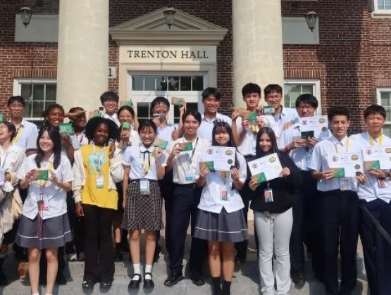
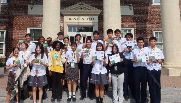
This summer, the SEMI Foundation brought together 16 high school students from Taiwan and four students from Pennsylvania for the inaugural SEMI Global Schools Academy, a five-day learning experience connecting sustainability, emerging technology, semiconductor careers, and global collaboration.The Academy is one part of the broader SEMI Global Schools model. Classroom and school-based programs give students opportunities to explore semiconductors, sustainability, artificial intelligence, and related careers where they already learn. The Academy builds on that approach by giving a smaller group of students a deeper opportunity to learn across institutions and communities.Students used Micro:bit sensors and AI-driven data analysis to explore environmental challenges including air quality, flooding, wastewater, and sea-level rise, with hands-on activities ranking among the most highly rated parts of the Academy.Following the Academy, nine in 10 participating students reported interest in the semiconductor industry—an encouraging indication that meaningful exposure can help young people see possibilities they may not have previously considered. Connecting Institutions Across BordersWhat made the Academy possible was not a single organization or campus, but a network of institutions working together.In Taiwan, schools, educators, government partners, and advisers helped prepare and support the participating students. In the United States, universities, local governments, educators, community organizations, and industry partners contributed expertise and learning opportunities.SEMI Global Schools serves as a connector across that ecosystem, bringing together institutions that already have strong relationships with students, communities, technology, and the semiconductor industry.That approach also makes the model adaptable. Rather than creating something entirely new in every region, Global Schools can build on the schools, universities, government partners, community organizations, and companies already there.Learning Through Technology, Sustainability, and CommunityStudents began their week at The College of New Jersey, where a sustainability professor from the New Jersey Institute of Technology (NJIT) introduced climate change, systems thinking, and the United Nations Sustainable Development Goals.Throughout the week, students explored artificial intelligence, semiconductors, sensors, coding, micro:bits, environmental monitoring, and data. They considered how technology might help address real-world challenges involving air quality, energy, transportation, infrastructure, and community well-being.The goal was not to turn students into semiconductor experts in five days. It was to help them understand that the technologies they use every day are connected to a much larger ecosystem—and that there are many different ways to participate in it.Students also learned that the semiconductor workforce extends beyond engineering to areas including sustainability, data science, supply chain, business, communications, education, public policy, and workforce development.Learning Beyond the ClassroomThe Academy also gave students opportunities to experience that ecosystem firsthand.Students learned at The College of New Jersey and the New Jersey Institute of Technology, participated in outdoor environmental learning at the New Jersey School of Conservation, visited Princeton University, and engaged with technology and semiconductor professionals.They also interacted with Princeton Mayor Mark Freda and Chester Mayor Stefan Roots, connecting their learning to broader conversations about education, technology, workforce development, and community opportunities.Just as importantly, Taiwanese and American students worked together throughout the week, sharing perspectives, solving problems, and learning across cultural and language differences.Building on What Already WorksThe Academy is one part of a broader Global Schools model that also includes classroom and school-based programs. Those programs can reach students where they already learn, while experiences like the Academy provide a deeper opportunity to engage across institutions and communities.The inaugural Academy offered an early example of what that model can look like: students from Taiwan and Pennsylvania learning together about sustainability, AI, semiconductors, and community challenges while engaging universities, industry, educators, and civic leaders.As the semiconductor industry grows globally, helping young people understand that ecosystem earlier matters.That is the vision behind SEMI Global Schools: connect strong institutions and create meaningful opportunities for more students to see where they might fit in the technology workforce of the future.As the semiconductor industry expands, workforce development, education, community capacity, and strong local institutions will increasingly be part of the infrastructure that supports sustainable growth.Learn more about the SEMI Foundation and SEMI workforce development programs addressing the global semiconductor industry’s talent gap.AcknowledgmentsDr. Prabhakar Shrestha, Assistant Director of Sustainability, New Jersey Institute of TechnologyRandall Solomon, Executive Director, Sustainable Jersey for Schools The New Jersey School of ConservationMelissa Taggart, Senior Director, Project Learning Tree Development and StrategyMary Westlund, Manager, Education Systems, Project Learning TreeBia Hamed, Ph.D., is Program Manager, Global Education Initiatives at the SEMI Foundation, Dr. Yi-Hsuan (Tim) Hsu is Adjunct Professor at National Tainan University in Taiwan, and Justin Harris is Senior Advisor for Climate Equity Social Impact at SEMI.
Read More
The European Chips Diversity Alliance (ECDA), a European Union-funded initiative coordinated by SEMI Europe, hosted the third Inclusive Chips Forum Bratislava: Bridging Education and Industry for Inclusive Talent at the Faculty of Electrical Engineering and Information Technology of the Slovak University of Technology in Bratislava on September 2, 2026. Co-organized with ECDA project partner Comenius University in Bratislava, the forum brought together educators, industry representatives, policymakers, and researchers to explore how collaboration between academic institutions and employers can open the semiconductor sector to a broader, more inclusive talent pool.The event addressed questions at the heart of Europe's semiconductor ambitions: how universities and employers can work together to attract and retain talent that is too often overlooked, what role institutional culture and leadership play in creating genuinely inclusive environments, and which models of cooperation are already proving effective across Europe and Slovakia. Through presentations, panel discussions, and exchanges of good practice, participants explored concrete approaches to building pathways into the semiconductor sector for people with a wide range of backgrounds and experiences. “Europe's semiconductor future depends on its ability to draw on the full depth of its talent,” said Cassandra Melvin, Senior Director, Business Development and Operations at SEMI Europe. “That means breaking down the barriers between education and industry, and making sure that the people who have historically been left out of this sector have a real path in."The program featured perspectives from across the ecosystem: from the counselling and psychological support systems that help students with diverse needs thrive in higher education, to the sharp decline in female enrolment at technical schools over recent decades, to what it means to build a semiconductor workforce that extends well beyond engineering. A closing panel, Connecting Education and Industry to Build Inclusive Semiconductor Talent, brought together representatives from SEMI Europe, the Czech and Slovak Semiconductor Centers, and onsemi Slovakia to discuss successful models of talent development and how education can better respond to the needs of a rapidly evolving sector.“Bringing educators and employers into the same room is necessary, not just useful,” said Janka Kottulová, Project Manager at Comenius University in Bratislava and co-organizer of the event. “The semiconductor sector cannot build the workforce it needs without universities and industry designing that future together, and forums like this one are where that work begins." SEMI Europe thanks the Slovak University of Technology in Bratislava, the Slovak Chips Competence Centre, and Comenius University in Bratislava for their partnership in organizing the Forum, with special thanks to Andrea Fábiková and Janka Kottulová for coordinating the event and its program.The Inclusive Chips Forum Bratislava is part of a series of events organized under the ECDA project, bringing together stakeholders across Europe to advance inclusion in the semiconductor sector. Information on upcoming forums will be announced shortly.About the European Chips Diversity AllianceThe ECDA is a collaborative initiative comprising 11 partners across Europe. ECDA works to expand access to training and employment in microelectronics by removing barriers for underrepresented and underserved communities, helping unlock the full spectrum of Europe's talent pool. Learn more at diversityinchips.eu or follow us on LinkedIn or Instagram. Frequently Asked QuestionsWhat is the Inclusive Chips Forum?The Inclusive Chips Forum is a series of public events organized by the ECDA bringing together educators, industry representatives, policymakers, and researchers to explore how diversity, equity, and inclusion can strengthen Europe's semiconductor talent pipeline. Each forum is hosted in a different European location and focuses on practical approaches to building more inclusive pathways into the sector.What topics were covered at the Inclusive Chips Forum Bratislava?The forum covered a wide range of topics, including inclusion practices in universities and companies, counselling and psychological support as tools for inclusion in higher education, gender representation in technical schools, diverse career pathways into the semiconductor sector beyond engineering, and how education and industry can collaborate more effectively to attract and retain underrepresented talent.Who attended the Inclusive Chips Forum Bratislava?The forum brought together educators and education managers from higher education and vocational training institutions, HR professionals and company representatives from the semiconductor sector, policymakers, and researchers from across Slovakia, Czechia, Austria, and wider Europe.How can educators and industry representatives get involved with ECDA?Organizations and individuals can engage with ECDA through its events, training programs, and online resources at diversityinchips.eu. ECDA welcomes participation from academic institutions, companies, and public bodies across Europe committed to building a more inclusive semiconductor workforce.When is the next Inclusive Chips Forum?Information on the next Inclusive Chips Forum will be announced shortly. Follow ECDA on LinkedIn and Instagram or visit diversityinchips.eu to stay up to date.Marta Scandella is Communications Coordinator for EU Projects at SEMI Europe.
Read More
The SEMI Quality Benchmark Consortium (QBC) met August 19–20 at Texas Instruments (TI) in Dallas, bringing together quality leaders from across the semiconductor industry to benchmark best practices and address common manufacturing challenges.Fern Yoon, VP of World Quality at Texas Instruments, hosted the latest face-to-face meeting, bringing together representatives from Infineon Technologies, STMicroelectronics, NXP Semiconductors, GlobalFoundries, and Intel Corporation for two days of technical discussions, benchmarking, and knowledge sharing.The QBC operates on a "give-to-get" philosophy, with members contributing survey data and participating in open discussions to build a shared library of industry best practices. This meeting centered on three topics: audit programs, failure analysis, and multi-source fab qualification.The office of Jack Kilby, inventorof the Integrated Circuit in 1958The meeting opened with an overview of Texas Instruments' business, global manufacturing footprint, and quality organization. Attendees also had the opportunity to tour Jack Kilby's historic office, offering a glimpse into the legacy of the co-inventor of the integrated circuit and the innovations that helped shape the semiconductor industry. Benchmarking Audit Programs and Quality SystemsThe first benchmarking session focused on internal audit programs and quality management systems. Participants compared how their companies qualify auditors, structure audit organizations, and comply with quality management standards. The discussion also covered supplier audits, management reviews, customer audits, and ways to improve audit effectiveness while reducing duplicate effort. Sharing Best Practices for Failure AnalysisThe second session focused on Electrical-Induced Physical Damage (EIPD), Electrical Overstress (EOS), and No Trouble Found (NTF) investigations. Participants compared failure analysis workflows, stress testing methods, customer communication practices, and criteria for closing investigations. Strengthening Multi-Source Fab QualificationWith manufacturers continuing to expand production capacity, multi-source qualification remains an important priority. Members compared strategies for technology transfer, risk assessment, customer communication, and qualification planning to demonstrate equivalent manufacturing capability across multiple fabs.Looking AheadThe meeting concluded with an update from the AI Product Quality Working Group, which is finalizing a white paper on AI-enabled Failure Mode and Effects Analysis (FMEA). Members also identified future benchmarking topics, including traceability, maverick lots, and quality at speed.Through open benchmarking and knowledge sharing, the SEMI Quality Benchmark Consortium continues to help members strengthen quality systems, improve manufacturing performance, and advance semiconductor quality across the industry. The consortium will continue its work at the upcoming meeting to be hosted by NXP in Eindhoven. Front row (left to right): Fern Yoon (Texas Instruments), Sumitra Sukumaran (Intel), Jens Luepke (Infineon), Lou Cerra (NXP), Roberto Lissoni (STMicroelectronics)Back row (left to right): Karim Somani (SEMI), Mark da Silva (SEMI), Eamonn McGovern (Intel), Mark Mason (Texas Instruments), Joe Beyer (NXP), Paul Tiner (Texas Instruments), Ivo Clerici (GlobalFoundries), Wesley Hirsch (TI)
Read More
The SEMI Startups for Sustainable Semiconductors (S3) program has announced 12 startups chosen as finalists for pitching to the industry at SEMICON West 2026 in San Francisco, California. The finalists were chosen from a field of 33 semifinalists after a virtual pitch event held over two days on July 29 and 30. Startups were evaluated by the organizing committee on five factors: the sustainability impact on our industry, commercial viability of product, company value proposition, the quality of the pitch and the startup team.The committee, made up of experienced Corporate Venture Capitalists (CVCs) from the global semiconductor industry and chaired by Micron, received submissions across four categories identified for 2026:Decarbonized Semiconductor ManufacturingDesign for Sustainability – Chips PackagingDatacenter Efficiency in Power Delivery and ThermalsNew Frontiers in Sustainable ComputingNow in its fifth year, the program is built around two strengths: exposure to semiconductor industry CVCs and the personal mentoring each startup receives. Mentoring topics are tailored to align with the greatest need of the startup and can range from a basic introduction to semiconductor manufacturing to connections with new funding sources. A full analysis of the program is available here.This year’s cohort spans six countries across four continents. The 12 finalists bring solutions across abatement, thermal management, water reuse, wafer inspection, power delivery, simulation, advanced packaging and memory architecture.The SEMI Startups for Sustainable Semiconductors pitch event will take place on the Sustainability Pavilion Stage on Wednesday, October 14, starting at 1:00 p.m. Andrew Byrnes, Director of Venture Capital for Artificial Intelligence at Micron Technology and chair of the S3 steering committee, will open the session and introduce the startup pitches.The finalist pitches will run through the afternoon, with each presenter given a 10-minute slot. Halfway through the pitch order, I will host a fireside chat with Steven Bakota, Corporate Vice President, Corporate Strategy and Corporate Development at Micron. The conversation will cover the role of startups in semiconductor sustainability and how they can build strong partnerships with large fabs.After the second group of pitches, votes for the winning startups will be tabulated during the S3 alumni panel, where past participants will inspire this year’s finalists with their stories of building partnerships in the semiconductor industry. An awards ceremony at 4:05 p.m., sponsored by Pangaea Ventures, will wrap up the S3 event and kick off the Sustainability Reception.Investors are welcome to attend the session at SEMICON West and to register their interest here to learn more about the 2027 program.2026 S3 FinalistsListed in presentation order.Rise Technology srlMilano, Lombardy, ItalyRise Technology develops next-generation semiconductor equipment based on its proprietary Dynamic Drop™ technology, overcoming the limits of conventional electroplating. The platform enables high-uniformity, high-throughput formation of interconnects, improving yield and enabling advanced architectures in heterogeneous integration, including chiplets, DRAM stacking, and 2.5D/3D packaging.KoolMicro, Inc.Dongtan, Gyeonggi-do, South KoreaKoolMicro is engineering the “Thermal Highway” for the AI era. The company develops Integrated Manifold MicroChannel (IMMC) modules that handle 4,000W and higher thermal loads. Its Direct-to-Chip solution uses vertically sprayed coolant to remove heat directly from the chip level, ensuring next-generation GPUs and CPUs never throttle.VEIR, Inc.Woburn, MA, USAVEIR develops superconducting power solutions, including cables and supporting infrastructure, from grid to rack.IWI Australia Pty LimitedSydney, NSW, Australia IWI Australia has developed and piloted a patent-pending catalytic quench of hydrogen peroxide in fab wastewater, particularly in complex water matrices with high peroxide load, extreme acidity and heavy metals. The company has also developed a patent-pending oxidation process for triazole, another pain point in fab operation and water reuse.enaDyneLeipzig, Saxony, GermanyenaDyne builds a fully electric, modular abatement system for semiconductor fabs based on non-thermal plasma catalysis. Its reactor destroys PFCs, VOCs, and NOx at greater than 99% destruction and removal efficiency through electron-impact chemistry at near-ambient temperature, fitting the same footprint as burn-wet for direct drop-in replacement. The same hardware extends to electrified chemical synthesis.Powerlattice Technologies Inc.Phoenix, AZ, USAPowerlattice has developed the first true monolithic integrated voltage regulator designed for high-wattage ASICs and XPUs operating above 1kW.UNISERSZurich, Canton of Zürich, SwitzerlandUNISERS has developed a novel wafer defect inspection and characterization technology to help fabs find and identify minute contaminants below 10nm, which are mostly invisible to currently used inspection equipment. As transistor nodes move to 3nm and below, these very small particles cause significant yield issues in state-of-the-art wafer fabs.CHIPADD, Corp.Binghamton, NY, USACHIPADD is the first to additively manufacture ultra-efficient copper cooling features directly onto the surface of GPU, CPU, and other high-power silicon chips. The company’s innovation includes materials and methods for robust bonding, manufacturing of solid and porous cooling features, enhanced materials for cooling, and manifold and precision jet design.FlexcomputeBoston, MA, USAFlexcompute builds a GPU-native physics simulation platform: Tidy3D for photonic and electromagnetic FDTD, PhotonForge for photonic design automation, Flexcompute RF for full-wave electromagnetics, and Flow360 for computational fluid dynamics and thermal analysis, delivering results 50 to 500 times faster than legacy CPU tools. FlexAgent, the company’s AI assistant, enables engineers to run and iterate simulations via natural language, accelerating chip and data center component design.HEXAspec Inc.Houston, TX, USAHEXAspec develops advanced molding compounds for semiconductor encapsulation using high-aspect-ratio hexagonal boron nitride nanosheets in polymers. Its scalable, patent-protected exfoliation process enables ten times higher thermal conductivity while maintaining electrical insulation, mechanical strength, and compatibility with standard OSAT and foundry packaging for HPC, automotive, and edge-AI applications.K1 SemiconductorChicago, IL, USAK1 Semiconductor creates engineered semiconductor wafers by peeling thin layers from high-quality single-crystal parent wafers. Its patented wafer splitting method releases a 5 to 50 micron-thick layer of single-crystal material from the parent wafer, which is then transferred and bonded to a handle wafer to create a custom semiconductor wafer.FS2Saint Louis, MO, USAFS2 is developing a monolithic 3D integration platform and memory, building next-generation stacked 3D SRAM and Process-on-Memory architectures. Its product delivers memory solutions with bandwidth, capacity, low latency, energy efficiency and cost advantages for AI workloads. Saifi Usmani is VP, Global Industry Sustainability Programs at SEMI.
Read More
For years, quantum computing has lived almost entirely in the research lab, but that is changing fast. The clearest sign of change came in spring of 2026, when IBM announced it would spin off Anderon as a standalone quantum foundry, separating its fabless chip design work from dedicated 300mm manufacturing. A company that had kept quantum fabrication tightly in house for over a decade realized that external demand now justified building a business around supplying wafers to others. When such a dominant incumbent decides to build a foundry business, that is a good indication the rest of the industry is not far behind.Over the past year, ATREG has spoken directly with a wide range of quantum hardware companies about their facility strategies. Nearly all of them are actively planning some form of scale-up, whether that means leasing cleanroom space, acquiring tools, or exploring options with existing fab operators. Alongside these conversations, we have tracked a wave of public funding rounds and cleanroom expansions from companies like QuantWare, IonQ, and IQM. Taken together, the pattern is unmistakable. Quantum computing is transitioning from a research curiosity into a manufacturing capacity question, and the companies driving this shift are bifurcating into two camps. These include vertically integrated players building or owning captive cleanrooms, and fabless designers routing wafers through commercial foundries. Both segments are now generating real fab transaction demand, which is relatively new.Why Now?Three forces are converging, with the first being government money. The U.S. Department of Commerce has signed letters of intent to invest roughly $2 billion into nine quantum computing companies in exchange for minority equity stakes. IBM’s Anderon spin-off and GlobalFoundries’ new quantum-focused business unit were granted the biggest incentives, while seven other venture-backed quantum hardware makers were granted smaller sums. Europe is moving in parallel, with France recently adding over €1 billion to its National Quantum Plan and Denmark building dedicated nanofabrication capacity for quantum chips near Copenhagen.Second, private capital is moving just as fast. Quantinuum's Nasdaq listing valued the company at over $15 billion. PsiQuantum's most recent raise pushed its valuation past $10 billion, and finally, IonQ's move to acquire SkyWater signaled that some fabless players are now willing to buy foundry capacity rather than wait for it. Third, although quantum computing is moving toward commercial production, the few specialized foundries capable of making quantum chips have already reached capacity with semiconductor demand. In discussions with foundry partners, we’ve learned that the U.S. Department of Commerce has received several proposals from companies looking for an industrialization partner and fab capacity for quantum manufacturing. Even before considering how many proposals ultimately get funded, the space available to absorb new quantum programs is limited. Separately, early company engagement is already happening well ahead of any formal facility buildout. This is a sign that demand is running ahead of infrastructure, and that latent demand is becoming active demand in real time. How Quantum Cleanroom Needs Compare to Traditional Fab Cleanroom RequirementsThe overlap with conventional semiconductor manufacturing exists, but it is narrower than the marketing suggests. Silicon-spin and superconducting modalities (the two furthest along commercially) map fairly directly onto standard 200mm-to-300mm wafer lines, running at mature nodes (16–28nm class) with no need for EUV lithography. While a qualified 200mm or 300mm metal deposition and etch line is one of the stronger brownfield fits available in the market today, quantum divergences can be seen in the following three areas. First, contamination control runs almost backwards from what logic manufacturers expect. For example, quantum fabs typically only need ISO 6 to 8 cleanroom classes. This is looser than what is standard for leading-edge logic, but specific materials like niobium, titanium nitride, and cobalt introduce isolation requirements that have nothing to do with particle counts. For instance, quantum hardware makers report that cobalt use in particular, creates friction with fabs built around conventional CMOS material rules. In addition, one major foundry noted that certain existing 300mm lines simply can't be converted for quantum work because of contamination risk from these non-standard materials.Second, packaging and assembly, not front-end fabrication, appears to be the primary roadblock. Bonding qubit chips to interposers, wiring for cryostats, and hybrid bonding require different tooling and tolerances than a front-end fab. In conversations with both foundry executives and quantum hardware companies, this stage was consistently described as the most fragmented and least mature part of the supply chain.Third, cryogenics and system integration are facilities problems, not cleanroom problems. Dilution refrigerators, cryostats, and helium supply require power capacity and vibration isolation more than particle control. In some cases, ISO 8 warehouse-grade space is sufficient. That reframes what "quantum-ready" facility space needs to look like, and it opens the door to buildings that wouldn't traditionally register as fab candidates.Where the Competitive Landscape is HeadedFewer than 100 meaningfully-funded quantum hardware companies exist today, but the small number of foundries qualified to serve them (including GlobalFoundries, imec, STMicroelectronics, Infineon, Tower, and SkyWater) are already seeing demand concentrate quickly. GlobalFoundries specifically, has emerged as an early plurality winner across multiple modalities. Whether that concentration holds, or whether scale-up costs push more players toward the SkyWater/IonQ model of outright acquisition, is one of the more consequential open questions in this space.What we are seeing in the market supports both scenarios simultaneously. Some companies are doing multi-year capacity planning well ahead of actual need, treating facility strategy as a long-lead problem to be solved early. Others are already outgrowing prototype-scale fabs and are looking to consolidate into shared or leased capacity. Both point to the same underlying reality: demand is forming faster than supply, and the packaging and assembly layer of the value chain remains particularly underserved.For a global industry built on brokering semiconductor fabrication assets, this is a familiar scenario with new variables. Brownfield capacity is a strong match for two of quantum computing's leading modalities today, with photonics and advanced packaging representing the next frontier. Ultimately, evaluating capacity gaps and moving before the rest of the market will be the next major opportunity for quantum computing's cleanroom moment. About Stephen M. RothrockStephen Rothrock is founder and CEO of ATREG, Inc. He founded ATREG in 2000 to help advanced technology companies divest and acquire infrastructure-rich manufacturing assets, including wafer fabs (front-and back-end) as well as MEMS, solar, display, and R D facilities. Over the last 25 years, ATREG has completed 40% of all global operational wafer fab sales in the semiconductor industry, representing a total of 60 transactions. Recent global acquisitions and dispositions have involved Allegro MicroSystems, Bosch, Elmos, Fujitsu, GlobalFoundries, IBM, Infineon, JDI, Maxim, Micron, Nexperia, NXP, onsemi, Plessey, Qualcomm, Renesas, Sony, Texas Instruments, TSI, VIS and more. Prior to founding ATREG, Rothrock established Colliers International’s Global Corporate Services initiative and headed the company’s U.S. division based in Seattle, Washington. Previously, he worked as director for Savills International real estate brokerage in London. There, he established the company’s corporate services platform serving large multinationals, many of whom were leading technology companies. Stephen also served on the U.K.-listed property company’s international board. He spent four years near Paris working for an international NGO. Stephen holds an MA degree in Political Theology from the University of Hull, UK and a B.A. in Business Commerce from the University of Washington in Seattle.
Read More
Daniele Pagano is a Project Manager at STMicroelectronics and standardization leader for the Heterogeneous Integration for Connectivity and Sustainability (HiCONNECTS) consortium, a coalition of 65 partners from 15 countries developing solutions for electronic components and systems. Through his work, Pagano is directly shaping the next generation of semiconductor manufacturing. SEMI spoke with Pagano about how integrating standards earlier in the development lifecycle can help bridge the gap between lab innovation and commercial deployment.SEMI: Could you tell us about your role at STMicroelectronics (ST) and what first drew you to semiconductor manufacturing?Pagano: At ST, I focus on advanced semiconductor manufacturing and innovation projects. I coordinate multidisciplinary teams, drive manufacturing development initiatives, and ensure that research outcomes translate directly into industrial applications.In parallel, I lead standardization activities focused on maintenance and cybersecurity for HiCONNECTS. These areas are central to our mission, which is to develop core technology solutions for heterogeneous integration. Through HiCONNECTS, we emphasize development in areas like RF infrastructure and IT data applications, which are quickly becoming the backbone of modern digital society. Semiconductor manufacturing attracted me because it combines science, engineering, and real-world impact. Semiconductors also underpin every technology we use today. They power everything from smartphones and electric vehicles to medical devices and industrial automation. I was also fascinated by the challenge of transforming cutting-edge research into innovations that are both highly scalable and reliable. SEMI: In HiCONNECTS, you're involved in both advanced manufacturing development and standardization. How do these two areas complement each other?Pagano: Both disciplines are closely interconnected. Advanced manufacturing focuses on creating technologies and processes that improve performance and reliability. Meanwhile, standardization helps ensure those innovations can be scaled. Without standardization, many promising technologies would struggle to move beyond the lab.Working across both areas within HiCONNECTS gives me a valuable perspective. As new technologies emerge, we can identify potential standardization needs early to ensure that available data is usable, complies with privacy and cybersecurity requirements, and can be broadly implemented across different applications. Daniele Pagano presenting at SEMICON Europa 2023SEMI: Your work explores areas like AI, digital twins, and data analytics. How do you foresee these technologies changing the way chips are produced over the coming years?Pagano: All of these technologies are becoming more crucial for the industry as semiconductor manufacturing processes get more complex. For instance, modern production environments generate large amounts of data, and AI can extract meaningful insights from that information to improve processes down the line. Digital twins are particularly valuable because they can generate virtual representations of entire production lines. They create a realistic environment for engineers to predict outcomes and improve operations without halting the entire production line. Within the HiCONNECTS project, new digital twins are being developed to optimize dispatching, scheduling, and shop floor productivity.Semiconductor factories will also become even more data-driven in the coming years, with higher levels of automation and real-time decision-making. Ultimately, digitization gives manufacturers greater freedom to produce the devices the world depends on. SEMI: Sometimes, standards are only considered after innovation. Why do you think it’s important to think about standardization throughout a research project like HiCONNECTS?Pagano: In reality, standardization should occur alongside innovation. When standards are considered at an earlier stage, researchers can better identify interoperability requirements, common terminologies, measurement methods, and best practices. However, due to the complexity of heterogeneous integration, addressing use-case requirements and standardization in tandem is key if we want to bring new technologies into production. To do this, we need cross-disciplinary collaboration. Ultimately, the goal can be broken into three steps. First, create innovative technologies in the lab. Second, ensure they can be successfully transitioned into high-volume manufacturing environments. And finally, leverage AI and digital twins to improve innovations over time. Standards play a crucial role in making all of that happen, and accomplishing each of these things is only possible when we work together. SEMI: HiCONNECTS brings together partners from industry, academia, and research organizations. What have you found most valuable about working in such a collaborative European project?Pagano: One of the greatest strengths of HiCONNECTS is our diversity of expertise. Industry partners contribute practical knowledge of manufacturing challenges and market needs, while academic and research organizations often bring fresh perspectives, novel methodologies, and deep scientific insights.Merging different disciplines also creates an environment where innovation can flourish. Challenges can be approached from multiple angles, and solutions benefit from more resources than any single organization can provide. From a personal perspective, I find the exchange of knowledge to be particularly valuable. Collaborative European projects like HiCONNECTS encourage openness, learning, and the creation of long-term professional networks. These relationships often continue beyond the life cycle of the project, and they help strengthen Europe’s semiconductor ecosystem. SEMI: Finally, what advice would you give to students and early career engineers who are considering a career in the semiconductor industry?Pagano: The first piece of advice is to embrace continuous learning. The semiconductor industry evolves rapidly, and new technologies emerge all the time. A strong foundation in engineering, physics, materials science, data science, or computer science can open several career opportunities in this field.Second, focus on developing strong technical abilities alongside effective collaboration skills. Modern semiconductor innovation relies on multidisciplinary teams, so the ability to communicate effectively and work across different domains is just as important as technical expertise.Lastly, do not underestimate the importance of resilience and problem solving. Semiconductor manufacturing is one of the most challenging engineering environments in the world, but it’s also one of the most stimulating. The technologies we develop directly impact society, so for anyone passionate about technology and innovation, it’s an exciting industry to build a career in. About HiCONNECTSHiCONNECTS (Heterogeneous Integration for Connectivity and Sustainability) is a three-year project bringing together 65 partners to develop sustainable, energy-efficient cloud and edge computing platforms. The project focuses on high-performance computing, storage infrastructure, network interfaces, and real-time analysis of IoT sensors and big data. SEMI Europe actively contributes to EU-funded initiatives, including Horizon Europe and Erasmus+ programs, capitalizing on its global member base and its role as the voice of the microelectronics industry. These activities enable SEMI to connect industry, research, and policy stakeholders while advancing European competitiveness and technological leadership. Learn more.Kartikey Srivastava is Lead of EU Projects at SEMI Europe.Daniele Pagano is Project Manager at STMicroelectronics Italy.
Read More
The SEMI Standards Team activities in Q2 focused on responding to the rapidly evolving needs of the microelectronics industry with critical revisions on key SEMI Standards. SEMI Standard F51, Guide for Elastomeric Sealing Technology, is a foundational standard for choosing and evaluating elastomeric seals. However, today’s manufacturing processes are demanding more seals with stronger chemical compatibility, lower particle and outgassing contribution, and other new and emerging considerations. SEMI is requesting industry feedback on F51 as part of its five-year review process. To participate in the next iteration of SEMI Standard F51, please complete the survey by October 15, 2026.Revisions are also underway for two important SEMI Standards. SEMI Standard E187, Specification for Cybersecurity of Fab Equipment, is currently being updated to include cybersecurity tiers based on application and need. Meanwhile, the revision to SEMI Standard E137, Guide for Final Assembly, Packaging, Transportation, Unpacking, and Relocation of Semiconductor Manufacturing Equipment, focused on an updated protocol that accounts for changes in the equipment handling environment. The revised version of E137, which included a title change, is being prepared for publication. The Korea Standards Team also hosted dedicated trainings for understanding and implementing SEMI S2, Environmental, Health, and Safety Guideline for Semiconductor Manufacturing Equipment. S2 covers the equipment used to manufacture, measure, assemble, and test semiconductor products, and it’s one of SEMI’s most widely referenced standards to date. With several new fabs coming online in 2026, SEMI Standard S2 is critical for establishing safety benchmarks ahead of tool installation. During Q2, the SEMI Water Management Group held a complimentary webinar that outlined its research findings for its two reports: Procedures Guide and Baseline and Water Savings Guide with Maturity Scale, and how the reports work with existing SEMI Standards. Some of these standards include SEMI Standard F98, Guide for Treatment of Reuse Water in Semiconductor Processing, and SEMI Standard F116, Guide for Drain Segregation for Semiconductor Manufacturing Tools to Support Site Water Reuse. The webinar can be accessed for free on demand. In addition, the SEMI Standards Team welcomed four new task forces chartered to respond to shifting industry demands. These task forces include the Flow Limiting Devices Task Force and the S2 Airborne Chemicals Task Force in North America, the Diagnostic Data Acquisition Task Force in China, and finally, the 310mm Square Panel Glass Carrier Task Force in Japan. Lastly, SEMI held 14 technical committee meetings in Q2 throughout Asia and Europe, with more than 20 standards either introduced or revised. To get involved in these SEMI Standards development efforts, become a member of the SEMI Standards Program. Membership is free. Feedback for SEMI Standard F51To adapt F51 to the modern manufacturing environment, the SEMI F51 Revision Task Force recently developed a feedback matrix outlining current priorities for this standard. For those working with elastomeric seals in any of the environments outlined on this webpage, please take a moment to provide additional input on which sealing characteristics, impurity concerns, and handling considerations should be most heavily considered in the revised version of F51. The SEMI F51 Revision Task Force is targeting a first draft by SEMICON West 2026, taking place from October 13-15. To have your feedback considered, please complete this survey by October 15, 2026. Revisions to SEMI Standards E187 and E137SEMI E187, Specification for Cybersecurity of Fab Equipment, is fundamental for outlining cybersecurity protocol for operating systems, network security, endpoint protection, and more. However, cyber threats are quickly evolving, and SEMI E187 will similarly need to be revised to address new and emerging concerns. One important revision to SEMI E187 is the introduction of three cumulative security levels (SLs), which will help equipment users and suppliers to select security profiles based on their needs. SL1 represents baseline compliance, while SL2 introduces stricter standards for equipment with greater exposure to cyber threats, like those with connections over public networks. Finally, SL3 is the most secure level of compliance, intended for applications with extremely sensitive assets to be protected. The revision of SEMI E187 represents an important step toward strengthening cybersecurity resilience across semiconductor manufacturing environments. The task force aims to advance this revision into the balloting stage this year, and continued industry participation will be essential to ensure that the final document reflects practical needs, global alignment, and broad technical consensus.Meanwhile, SEMI Standard E137, Guide for Final Assembly, Packaging, Transportation, Unpacking, and Relocation of Semiconductor Manufacturing Equipment, offers a reference for activities occurring between final assembly and moving equipment into a cleanroom. While today’s iteration covers recommended packing materials and step-by-step instructions for each subsequent process, it doesn’t account for changes in the equipment handling environment. In addition, the new version intends to be easier to understand while providing additional guidance on crating materials for specific circumstances. The revised document officially passed technical review and will be available soon. SEMI Korea S2 Safety Training From June 10-12, the SEMI Korea Standards Team hosted a SEMI Safety Standards training course. Divided into beginner and advanced sessions, the course offered a deeper understanding of safe semiconductor design and equipment evaluation. Held at the Suwon Convention Center in Suwon, Korea, it covered everything from safety standard basics all the way to in-depth explanations and practical implementation strategies for SEMI Standard S2. The June 10 program introduced the basics of SEMI Standard S2, explaining safety interlocks and emergency shutdown protocols, before diving into electrical design, fire protection, ergonomics, chemical, radiation, sound pressure, and more. For those more familiar with SEMI Safety Standards, the advanced course from June 11-12 provided more guidance on the installation of emergency stop and safety devices, chemical safety, machine safety, electrical design safety, and optimal risk assessment techniques. The advanced session went beyond SEMI Standard S2 and covered material related to SEMI Standards S6, S8, S10, S14, S17, and S28.The next SEMI Korea Standards course, SEMI Semiconductor Test Technology Training, will be held on September 9 in person at the same location. Apply today. Water Management Explanatory WebinarIn Q2, the SEMI Water Management Working Group held a webinar outlining its research for the Water Management Strategy Reports and explained how findings interact with SEMI Standards. The webinar covered procedure guidelines, water saving and baseline setting, and the solutions maturity scale. The reports were developed to help improve company water posture through recycling and reclaiming after implementing water saving strategies. They work to go beyond existing standards to help water managers understand water balance and set reasonable goals for new solutions. The reports can be downloaded here free of charge, and the webinar can be viewed on demand. New SEMI Standards Task Forces As the microelectronics industry continues to expand, four new task forces were developed in Q2 to address emerging needs. The Flow Limiting Devices Task Force was established in May 2026 to address issues identified during a reapproval ballot of SEMI S5, as well as other matters related to SEMI Standard S5 that are later identified. This task force is based and operated under the North America (NA) EH S Technical Committee Chapter. The revision to SEMI S5 was issued for ballot in Cycle 6-2026. The ballot results will be reviewed and discussed at the next task force meeting, which will be held in conjunction with SEMICON West 2026 in San Francisco, California.Also created in May, the S2 Airborne Chemicals Task Forcewill modify section 23.5 to require that the assessment criteria be demonstrated, but not necessarily during equipment evaluation. The task force leader believes that an equivalent level of safety can be achieved through alternative assessment methods. For example, industrial hygiene (IH) monitoring could be performed before opening a process chamber while personnel are wearing appropriate personal protective equipment (PPE). The results of the assessment would then determine whether PPE can be removed or should continue to be worn during subsequent work inside the chamber. This task force is based in North America and will fall under the EH S Technical Committee.Based in China, the new Diagnostic Data Acquisition Task Force will investigate problems with the implementation of Equipment Data Acquisition (EDA)/Interface A Standards in the China region and propose suggestions for improvement. This task force will also develop new SEMI Standards for EDA/Interface A and diagnostic applications as needed, in addition to promoting cooperation with other task forces in China involved with EDA/Interface A. This task force was approved in June and will fall under the China Information Control Technical Committee chapter. Finally, in response to a Line-Item Revision ballot for SEMI Standard 3D20, Specification for Panel Characteristics for Panel Level Packaging (PLP) Applications, that is being revised to include smaller panel sizes, the 310mm Square Panel Glass Carrier Task Force was formed on June 5 to revise SEMI Standard 3D23 to also include specifications for 310mm square glass carriers used in panel level packaging. Currently, 3D23 covers 510 x 515mm and 600mm x 600mm panel sizes. In its efforts to expand the standard, the task force will determine the length, width, thickness, and associated tolerances for the 310 mm panel, features like orientation corner and reference edges, backside ID mark location, and other necessary specifications. This task force is based in Japan and falls under the 3D Packaging and Integration Technical Committee. Interested in joining a task force? Apply for SEMI Standards membership.Outcomes from Q2 Technical Committee Chapter Meetings Q2 included several Technical Committee chapter meetings across Asia and Europe, where upcoming ballots and initiatives were discussed. To exchange ideas in real-time, a community page is now available on the Connect@SEMI platform. Japan Meetings The Automation Technology Japan Technical Committee met on June 19 and presented reports from the AI, Surface Mount Technology, and F-GEM task forces. The Information Control Japan Technical Committee convened on June 17 and approved SNARF 7476 , Guide for Maintenance Robot Communication.The 3D Packaging Integration Japan Technical Committee conducted ballot reviews on June 5 for a line-item revision to SEMI Standard G82-1115, Specification for 300 mm Load Port for Frame Cassettes in Backend Process, as well as a line-item revision to SEMI G95-1120, Specification for Mechanical Features of 450 mm Load Port for Tape Frame Cassettes in the Backend Process. The EHS Japan Technical Committee met on June 3 to present several task force reports, including one from the Global Seismic Protection Task Force, another from the Mobile Maintenance Robot Safety Task Force, and several more from various SEMI Standard revision Task Forces. The Gases and Facilities Japan Joint Technical Committee reviewed the revision ballot for SEMI Standard E137-0705 on May 29. The committee approved the revision and a title change. Once published, the Standard will be called Guide for Final Assembly, Packing, Transportation, Unpacking, and Moving of Semiconductor Manufacturing Equipment. The Physical Interface Carriers Japan Technical Committee proposed a new primary standard, Specification for Enhanced Handoff Interface, and a complementary subordinate standard, Specification for Modbus Communication for Enhanced Handoff Interface, on May 21. These documents passed review and are currently being processed for publication.The Liquid Chemicals Japan Technical Committee met on May 21 to present several task force reports, including Liquid Filter Task Force, Liquid-Borne Particle Counter Task Force, and Valve Fitting Task Force. Ballot 7267A, Revision to SEMI C77-0818 with title change to: Test Method for Determining the Counting Efficiency of Liquid-Borne Particle Counters for Which the Minimum Detectable Particle Size is in the Range of 20 nm and 100 nm, was authorized in Cycle 8-2026, which will be issued in late September.The Information Control Japan Technical Committee met on April 17 to report the Ratification Ballot results for Line-Item Revision to SEMI E170-0520, Specification for Secured Foundation of Recipe Management System (SFORMS) and SEMI E170.1-0520, Specification for SECS-II Protocol for Secured Foundation of Recipe Management System. This ballot passed, and both primary and subordinate standards will be available soon. The Silicon Wafer Japan Technical Committee convened on April 17 to review ballot 6570D for a new SEMI Standard, Guide for Measuring Bulk Micro Defect Density and Denuded Zone Width in Annealed Silicon Wafers by a Laser Scattering Tomography Technique. This document passed review and is currently being processed for publication.Korea MeetingsThe EHS Korea Technical Committee also met on June 19 to discuss its Field-Based Safety Subcommittee, Regulatory Alignment Subcommittee, Robot Safety Task Force, and S2 Major Revision Liaison Task Force.The Information Control Korea Technical Committee reviewed reports from the GEM300 Task Force, the Diagnostic Data Acquisition Task Force, and the Advanced Back-End Factory Task Force, on April 23.China MeetingThe Information Control China Technical Committee met on June 2 and approved SNARF 7475, Line Item Revision to E90-1224, Specification for Substrate Tracking and E90.1-1224, Specification for SECS-II Protocol Substrate Tracking. The goal is to help both equipment manufacturers and factories using E90 achieve precise and consistent information exchange regarding substrate state.Taiwan MeetingThe FPD Metrology Taiwan Technical Committee discussed and adjudicated ballot 7352, Revision to SEMI D056-0519, Test Method for Measurement for Ambient Contrast of Flat Panel Displays, which failed technical review, on May 22. The updated ballot 7352A is issued in Cycle 7-26 and is scheduled for review on November 20, 2026.Europe MeetingThe Compound Semiconductor Materials Europe Technical Committee met on April 14. Ballot 7111, Revision of SEMI M81-0418, Guide for Defects Found in Monocrystalline Silicon Carbide Substrates, passed technical review. The revised SEMI M81 standard is being processed for publication and will be available for purchase online.In Case You Missed It – Standards Suite Overview White Paper The SEMI Standards team released a complimentary, 23-page white paper, titled Selecting the Right Standards for Your Factory Use Case and Technology Needs. This paper covers four SEMI Standards Suites to support equipment communications and automation. It breaks possibilities into smaller groups of existing standards to help factories and suppliers scale more efficiently. Download the white paper. New and Revised Standards Released in Q2 April 2026May 2026June 2026Get InvolvedSEMI Standards development activities take place throughout the year in all major manufacturing regions. To participate, join the SEMI International Standards Program.SEMI Standards are available through individual download purchases or online via SEMIViews. Watch this video to learn more about how SEMIViews offers a cost-effective and streamlined way to access 1,110+ SEMI Standards. Sign up for a 30-day SEMIViews trial.For more information, please visit the Standards website and events page. For any questions regarding SEMI Standards activities, please contact your local SEMI Standards staff.Paul Trio is Director of Standards at SEMI.
Read More