downloadGroupGroupnoun_press release_995423_000000 copyGroupnoun_Feed_96767_000000Group 19noun_pictures_1817522_000000Member company iconResource item iconStore item iconGroup 19Group 19noun_Photo_2085192_000000 Copynoun_presentation_2096081_000000Group 19Group Copy 7noun_webinar_692730_000000Path
Skip to main content
Default Banner Image

Clark Tseng

SEMI’s annual Surface Preparation Cleaning Conference (SPCC) brought industry experts to Chandler, Arizona, to address the biggest challenges affecting this area of the semiconductor industry. As the premier technical forum dedicated to advancing surface preparation, cleaning technologies, and wet processes, the conference featured dozens of speakers who shared insights on the current market, emphasizing key themes like advanced packaging, power delivery, advanced DRAM, sustainability, and more.Ahead of this year’s conference, SEMI and Global Net Corp. (GNC) developed a new report, Glass Core Substrate Market and Development Trends, examining manufacturing challenges, supply chain structure, and market outlooks through 2040. This resource helps organizations evaluate the glass core substrate landscape before committing to production. A sample of the report is available for complimentary download. High-Level Updates and SEMI Insights Joe Stockunas, president of SEMI Americas, kicked off SPCC 2026 by announcing that the industry is entering its biggest era yet, on pace to reach $1 trillion in annual revenue in 2026 – 4 years ahead of prior forecast. The semiconductor industry has become the third most valuable global industry with top companies' market capitalization surging over the past decade. By 2030, industry analysts expect annual revenue to soar to $1.9 trillion, driven largely by demand for AI infrastructure, with logic and micro capacity also expected to nearly double. However, Stockunas also noted headwinds including geopolitical tensions and a growing talent shortage.Duncan Meldrum from Hilltop Economics offered a cautionary macroeconomic view, warning that AI growth is now concentrated among a handful of hyperscalers and leading-edge chipmakers, creating concentration risk. Geopolitically driven inflation is squeezing consumers, while supply chain disruptions are impacting critical materials like sulfuric acid, helium, and tungsten. Meldrum also highlighted concentration risk in production, with a few ODMs and manufacturers dominating the AI server market.SEMI analyst Inna Skvortsova provided materials market updates, emphasizing that advanced devices are driving materials intensity per wafer. Lithography, wet chemicals, and CMP are already seeing double-digit growth, led by increasing number of processing steps, rising count of EUV layers, and tightening CMP process windows at advanced nodes. Deposition materials were noted as another fast-growing segment that is forecast to grow at a 13.5% CAGR through 2030, driven by molybdenum adoption and backside power networks. Furthermore, introduction of new materials, including Ruthenium and Tungsten Carbon Nitrite (WCN) hardmasks, brings new opportunities and challenges with regards to wet processes.On memory, Skvortsova confirmed that AI pull has made memory a compute-stack bottleneck, driving capital toward leading-edge logic and HBM. Logic and micro capacity nearly doubles by 2030, but growth is highly concentrated in advanced nodes (≤7nm) pressuring non-AI segments.Skvortsova also highlighted a supply chain shift from globalization to localized production networks, with China emerging as a significant player in areas like bulk wet chemicals, gases, and deposition materials. While alternative sources are emerging, supplier re-qualification may result in higher material costs.Theme 1 - Hybrid Bonding FluxSPCC 2026 highlighted cleaning innovations for hybrid bonding, a core technology enabling AI scaling and glass core substrates. Srini Raghavan (ProSys) presented a paper based on the collaborative work between Intel and ProSys in the area of megasonic removal of flux from narrow gaps in advanced packaging structures. His team found that application of 10 msec pulses of 925 kHz sound wave at 90% duty cycle was very effective in flux removal in a semi-aqueous formulation Acoustic streaming rather than cavitation appears to be the primary cleaning mechanism under the test conditions.Koji Nakata (Kurita Industries) tackled particle contamination, copper corrosion, and chemical consumption in 3D stacking. His solutions include:Functional water + megasonic cleaning for higher particle removal than SC-1.Alkaline water rinsing to reduce copper pad recessing vs. DI water.Functional water to lower chemical consumption, cost, and environmental impact.Theme 2 – Wet Etch, Gate-All-Around, SelectivityTwo presentations highlighted next-gen logic wet etch challenges. IBM's Alma Vela Ramirez showed that an oxide-selective wet chemistry reduced buried void defects by over 20× during dummy gate polysilicon removal in GAA nanosheet flows. From her findings, chemistry 1 showed higher defectivity, while chemistry 2, selective to gate oxide and compatible with spacers, drastically reduced void formation by preserving the bottom oxide layer.Mitsubishi Chemical Corporation’s Tomoki Nara demonstrated a Si/SiGe selective etchant achieving a record 750:1 selectivity, critical for protecting thin SiGe layers during Si thinning in backside power delivery networks (BSPDN). His new alkaline wet etchant and single-wafer spin process address conventional etchants' inability to stop cleanly on SiGe, significantly expanding the process window during Si thinning and reducing the risk of SiGe damage.Theme 3 – Scaling DRAM to Advanced NodesMicron presented two DRAM manufacturing breakthroughs. Shihui (Adara) Yang introduced a dilute sulfuric peroxide clean achieving 3.59× BCF:TCF (bottom container fill and top container fill) selectivity—solving uniformity issues where conventional fluorine-based chemistries etch both layers at similar rates, causing container shorts and yield loss at advanced nodes.Hiroki Uoyama introduced a wafer backside polishing brush incorporating diamond or silicon carbide, achieving over 90% defect height reduction with no wafer thickness loss. This physical cleaning approach improves focus control, alignment accuracy, and overall yield — critical as lithography margins narrow dramatically at smaller nodes.Theme 4 – Sustainable Materials Stripping Solutions Sustainability was another core focus at SPCC 2026, with three distinct approaches taking center stage — each addressing a different facet of environmental impact in the fab.PFAS are among the major pollutants in semiconductor manufacturing waste streams, whose separation and destruction are challenging. As demonstrated by imec’s Sina Kaabipour, representing the collaborative research work between imec, Purdue University, and Enspired Solutions, UV destruction can achieve more than 99% PFAS destruction efficiency for simulated semiconductor manufacturing waste, showcasing great potential for scale-up and direct mineralization from liquid fab waste effluents.Diane Bijou from Technic launched TechniStrip® Micro 680, an NMP-free stripper with sub-2-minute stripping time, better loading capacity, extended bath life, and lower cost per wafer than NMP/amine-based strippers.Chihiro Kobata of JSR unveiled a water-rich stripper removing both photoresist and spin-on glass without NMP, DMSO, and TMAH, at lower temperatures (40–60°C), with ECO conscious, high performance, and high material compatibility and fab-part compatibility.Connect With SEMI SEMI would like to thank all speakers, sponsors, and attendees for the success of SPCC 2026. Download a preview of SEMI and GNC’s new report, Glass Core Substrate Market and Development Trends, and stay connected with SEMI on LinkedIn and X. Clark Tseng is Senior Director of Market Intelligence at SEMI.
Read More
The global economy has started down a gradual path to recovery from COVID-19 in recent months as the world continues to combat the virus. Yet one sector – semiconductors – has shown impressive growth powered by a transformation hastened by the pandemic across industries ranging from education and work-from-home to healthcare.Semiconductor sales increased 12% in September to mark a second consecutive month of double-digit growth, and year-to-date semiconductor receipts as of September jumped 5.5% compared to the same period in 2019, according to SIA/WSTS.While this upward trajectory is encouraging, it pales compared to 2020 semiconductor equipment billings growth, with results from SEMI showing worldwide global chip equipment billings in September soaring to a new high of $7.6 billion this year. During the first nine months of 2020, aggregate equipment billings logged a 23.6% rise compared to the same stretch in 2019, surpassing $51 billion. Better still, the total semiconductor equipment market in 2020 is on track to beat the previous high of $64.5 billion set in 2018.Investments in China, Taiwan and Korea are fueling the chipmaking equipment spending surge. With big domestic and international fab projects in the works, China this year is projected to become the world’s largest capital equipment market for the first time, surpassing Taiwan, which will follow at a close second. Korea will rank third in equipment investments. Taiwan and Korea growth will come on the strength of equipment spending for manufacturing leading-edge semiconductors.Equipment billings in North America and Europe declined year-over-year as the automotive and industrial sectors suffered the heaviest blows from COVID-19. Investment momentum in both regions is expected to pick up in 2021 after automotive production recovers to pre-pandemic levels while factory automation will boost industrial demand.For more information about monthly equipment billing trends by region and equipment segment, please see the SEMI Equipment Market Data Subscription.Clark Tseng is director of Industry Research and Statistics at SEMI.
Read More
Region’s Fab Capacity Expansion Picks up PaceUnwavering in its drive to build a strong, self-sufficient semiconductor supply chain, China plans more new fab projects than any other region in the world from 2017 to 2020, and its expansion of fab capacity recently picked up pace on the strength of new foundry and memory projects from both domestic and foreign companies, according to SEMI’s 2018 China Semiconductor Silicon Wafer Outlook report. China’s installed fab capacity is forecast to grow at a 12 percent CAGR from 2.3 million wafers per month (wpm) in 2015 to 4 million wpm in 2020, faster than all other regions.Well known for its semiconductor packaging prowess, China in recent years shifted its focus to front-end semiconductor fabs and a few key material markets. In 2018, the region’s surge in fab investment thrust it past Taiwan as the second largest capital equipment market in the world, behind only Korea. However, China’s semiconductor manufacturing growth faces strong headwinds. Chief among them is the tight supply of silicon wafers over the past two years due in large part to the sector oligopoly’s firm control of global production, with the top five wafer manufacturers accounting for over 90 percent of market revenue. In response, China’s central and local governments has made the development of its domestic silicon wafer supply chain a key initiative, funding multiple silicon wafer manufacturing projects.According to the 2018 China Semiconductor Silicon Wafer Outlook report, many of China’s domestic silicon suppliers capably provide wafers 150mm in size and smaller. And the while the region lags peers in 200m and 300mm processing technology and capacity, strong domestic demand and favorable policies have fueled progress in 200mm and 300mm silicon manufacturing with some Chinese suppliers having reached key large-diameter manufacturing milestones.However, it will take these new suppliers several years before they can meet capacity and yield requirements of the larger-diameter silicon wafer market. Company plans and announcements indicate that by the end of 2020, total silicon supply capacity in China will reach 1.3 million wpm for 200mm, possibly leading to a slight oversupply, and 750,000 wpm for 300mm.China’s equipment suppliers, particularly crystal furnace vendors, are also investing in the development of 300mm wafer manufacturing, and domestic tool suppliers have developed most of the necessary tools for wafer manufacturing, except for inspection.While China’s silicon wafer suppliers continue to lag international peers in manufacturing capabilities, the region’s silicon manufacturing ecosystem is maturing and becoming better integrated. The sector’s growth is driven and accelerated by significant domestic market demand and favorable policies.About the China Semiconductor Silicon Wafer OutlookSEMI’s 2018 China Semiconductor Silicon Wafer Outlook is a comprehensive research report with a Microsoft Excel® workbook containing in-depth analysis of China’s silicon wafer manufacturing ecosystem as it relates to the global semiconductor wafer industry. The report covers the latest developments in China’s silicon wafer supply chain, including details on the rise of China’s silicon manufacturing, polysilicon, and silicon wafer-related equipment companies. The report also examines policies, funding and their implications for China’s silicon wafer supply chain.Clark Tseng is director in Industry Research and Statistics at SEMI.
Read More
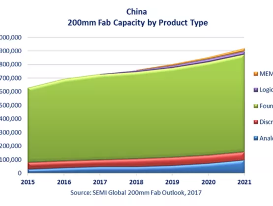
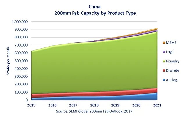
By Clark Tseng, Industry Research Statistics Group, SEMI China’s ambitious plans to build a world-class semiconductor manufacturing supply chain domestically certainly has the industry’s attention. With over a dozen new 300mm fab announcements lately from Foundries, DRAM, 3D NAND, and as well as CMOS image sensor companies (either from international semiconductor makers or from indigenous players), China has launched a huge investment in wafer fab capacity that is expected to ramp in the next five years. While advanced 300mm fab investment attracts most of the attention and resources, China does not skimp on the more “matured” 200mm fabs. China will have the most new 200mm fab projects and capacity additions in the next few years compared to other regions. According to SEMI’s latest 200mm Fab Outlook report, China currently has about 700,000 wafers per month (wpm) installed fab capacity, and this is forecasted to surpass 900,000 wpm by the end of 2021, or over 28 percent growth in five years. By then, China’s 200mm capacity is expected to surpass America, Japan, and Taiwan, and be second only to Europe. A further examination of China’s new 200mm fab projects shows a wide diversity in products. Beyond the usual 200mm foundry investment led by SMIC and Hua Hong Semiconductor, an increasing number of new projects are focusing on analog, power, and MEMS applications. According to SEMI’s latest 200mm fab Outlook report, China will add eight new 200mm volume fabs between 2016-2021: two for foundries, two for analog, two for MEMS, one for power, and one for logic. In the meantime, China is not limiting itself to adding wafer capacity. It is also developing material and equipment capabilities around 200mm wafer manufacturing. A number of silicon wafer suppliers are emerging in China targeting 200mm and smaller wafer markets. On the equipment side, the 200mm tool availability remains the biggest challenge for the industry in adding more 200mm capacity; some projects have been postponed because of it. China equipment suppliers are expected to take the opportunity to develop the tool sets needed to satisfy the upcoming demand for these fabs. China’s 200mm capacity will evolve to make more than “legacy” products, e.g., smart card, Analog IC, and Discrete IC. These manufacturers will become more versatile advancing into MCU, PMIC, CIS, fingerprints sensor, power, MEMS, and other devices. With the rise of China’s electronic OEMs and automakers, these 200mm fabs will play an even more important role supporting various manufacturing ecosystems in China. For more information, visit https://discover.semi.org/global-200mm-fab-outlook-registration.html
Read More