downloadGroupGroupnoun_press release_995423_000000 copyGroupnoun_Feed_96767_000000Group 19noun_pictures_1817522_000000Member company iconResource item iconStore item iconGroup 19Group 19noun_Photo_2085192_000000 Copynoun_presentation_2096081_000000Group 19Group Copy 7noun_webinar_692730_000000Path
Skip to main content
Prior to 1997, the industry enjoyed the “mask maker’s holiday” when IC feature sizes were larger than the lithography wavelength and the industry enjoyed the number of transistors per area doubling for no additional cost. This era ended when 248nm lithography was adopted. 248nm lithography enabled device manufacturers to extend traditional optical lithography but forced the adoption of resolution enhancement techniques such optical proximity correction and phase shift masks. 193nm lithography was introduced for 90nm features and the industry was required to adopt increasingly complex strategies to shrink device geometries further such as liquid immersion, double patterning, and more recently multiple patterning. These techniques have enabled device manufacturers to extend traditional optical lithography while next-generation lithography approaches, including extreme ultraviolet (EUV), maskless lithography, and nanoimprint remain in the background.EUV is the most favored next-generation lithography and has received the lion’s share of press and research dollars. EUV was initially scheduled to be used for 65nm feature processing but persistent challenges with this technology remain unsolved. Key obstacles associated with EUV are: finding adequate source power, EUV photoresists, and developing mask manufacturing infrastructure. Significant progress has been made and there are now beta EUV tools in the field. The extended delay of EUV forced chipmakers to extend 193nm immersion lithography with multiple patterning down to sub-10nm. With so much invested in optical lithography, even when EUV is ready, it is expected that chip makers will use a combination of EUV and 193nm immersion with multi-patterning for leading-edge devices.The delay in EUV for volume production has impacted the photomask market. Last month, SEMI reported that the worldwide semiconductor photomask market recorded a record high in 2016, reaching $3.32 billion. SEMI also noted that captive mask suppliers have significantly increased their market share due to the capital intensity required by leading-edge manufacturing.It remains to be seen what lithography solutions the industry will implement to maintain Moore’s law as the costs of advanced lithography increase faster than increased device density gains. What is clear is that the photomask market is mature and that captive shops, with their deep pockets, are assuming an increasingly important role. Still merchant shops continue to serve a vital function by servicing standard mask sets and providing manufacturing capability in the event of a service disruption.A recent SEMI published report, Photomask Characterization Summary, provides details on the 2016 Photomask Market for seven regions of world including North America, Japan, Europe, Taiwan, Korea, China, and Rest of World. The report also includes data for each of these regions from 2003 to 2018 and summarizes lithography developments over the past year.Please click here to download a copy of the SEMI Photomask Market Characterization Executive Summary. For information on all SEMI Market Information, visit: www.semi.org/en/MarketInfo.
Read More
They're calling it, “The most advanced, lowest power-consuming GPU-enabled MPU on the market.” It's NXP's new i.MX 7ULP general-purpose processor, and it's on 28nm FD-SOI. They've got a nifty video summing it all up – you can watch it here. [caption id="attachment_10388" align="alignleft" width="300"] NXP is first to market with a general-purpose processor on FD-SOI: the i.MX 7ULP. It's got both ultra-low power consumption and rich graphics for battery powered applications. (Courtesy: NXP)[/caption] With the i.MX 7ULP, NXP is first to market with an FD-SOI applications processor offering the industry’s lowest power consumption. The debut was made at the recent Embedded World Conference in Nuremberg, Germany, and it made a big splash in media across the globe. (Read the full press release here.) In deep sleep mode, it boasts power consumption of just 15 uW or less: 17 times less than previous (and highly successful) low power i.MX 7 devices. Dynamic power efficiency is improved by 50 percent on the real-time domain.The i.MX 7ULP applications processor family is currently sampling to select customers. Broader availability of pre-production samples is scheduled for Q3 2017.Hello, IoT!The high-performance, low-power solution is optimized for customers developing applications that spend a significant amount of time in standby mode with short bursts of performance-intense activity that require exceptional graphics processing. Sounds like IoT – and indeed it is, and more.With the i.MX 7ULP, NXP's targeting wearables, portable healthcare, smart home controls, gaming accessories, building automation, general embedded control and IoT edge solutions. Bottom line: it's designed to enable ultra-low-power and secure, portable applications – especially those demanding long battery life. (Read the current fact sheet here.)The detailsThe i.MX 7ULP features an advanced implementation of the ARM® Cortex®-A7 core, the ARM Cortex-M4 core, as well as a 3D and 2D Graphic Processing Units (GPUs). It's got a 32-bit LPDDR2/LPDDR3 memory interface and a number of other interfaces for connecting peripherals, such as WLAN, Bluetooth, GPS, displays, and camera sensors. [caption id="attachment_10387" align="alignnone" width="834"] (Courtesy: NXP)[/caption] NXP says this new design, based on FD-SOI’s lower voltage capability, enables rich user experience through extremely power-efficient graphics acceleration, a fundamental requirement in many of today’s consumer and industrial battery-operated devices that incorporate robust graphic interfaces. Further enablement includes rich Linux or Android ecosystem with the real-time capability supported by FreeRTOS.Leveraging body biasing and moreNXP credits the design’s extreme low leakage and operating voltage (Vdd) scalability to that FD-SOI specialty: reverse and forward body biasing (RBB/FBB) of the transistors, and its smart power system architecture.In presenting the new i.MX 7ULP to the tech press, the company highlighted the following FD-SOI design advantages: Large dynamic gate and body biasing voltage range Domain and subsystem optimization with custom standard cell library with mixed voltages Low quiescent current (Iq) bias generators Enhanced ADC performance with unique FD-SOI attributes Fail Safe I/O for simplified low power system design To that, add a note about security. As the chip's fact sheet says, “The processors deliver hardware-enabled security features that enable secure e-commerce, digital rights management (DRM), information encryption secure boot, and tamper detection.” Those are just the sort of things that demand the bursts of high performance that dynamic forward body biasing delivers where and when it's needed.Samsung fabs, Verisilicon adds IPTwo other SOI Consortium members – Samsung and Verisilicon – are particularly pleased with NXP's results.“We are excited that NXP is the first to bring the benefits of FD-SOI (28FDS) technology to the general purpose market,” says Ryan Lee, VP of the Foundry Marketing Team at Samsung Electronics. “28FDS technology will satisfy a growing and critical need for ultra low power designs that require power-performance at very low voltages. We plan to evolve 28FDS technology to a differentiated low-power single platform by implementing RF and embedded Non-Volatile Memory (eNVM) solution for our customers’ success.”NXP’s processor design enables robust low power graphics for the IoT and wearable markets through two graphic processor units (GPU) from Vivante: the GC7000 NanoUltra 3D GPU with a low power single shader, and the GC320 Composition Processing Core (CPC) for 2D graphics. The 3D GPU plays a critical role in enabling rich 3D based user interfaces, while the CPC can accelerate both rich 3D and simpler 2D user interfaces. Processors based on the combination of the two GPUs enable efficient display systems which offload and significantly reduce system resources, in turn providing rich user interfaces at low power levels to extend the battery life of devices.“Our 3D GPU is a result of a joint collaboration between Vivante and NXP to deliver industry-leading 3D capabilities with the lowest power consumption,” said Wei-Jin Dai CEO at Vivante Corporation and Chief Strategy Officer and GM of the IP Division at Verisilicon. “The power savings from using the right GPU in an ultra low power processor is one of the major attributes and advantages of the architecture.”So, now shall we dig in a little deeper into the “why FD-SOI” question? Read on in Part 2 of this article.-- By Adele Hars, ASN Editor-in-Chief
Read More
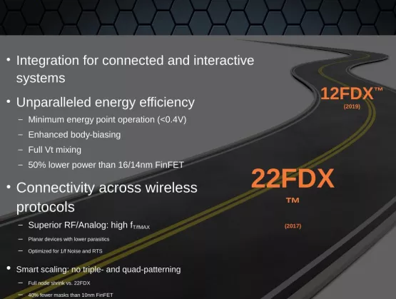
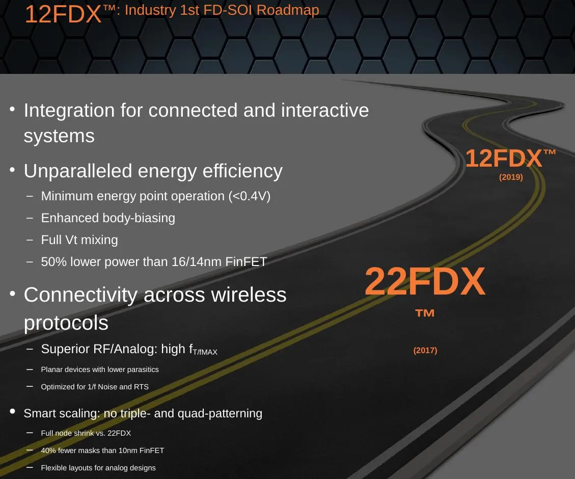
12nm FD-SOI has now officially joined the GlobalFoundries’ roadmap, targeting intelligent, connected systems and beating 14/16nm FinFET on performance, power consumption (by 50%!) and cost (see press release here). Customer product tape-outs are expected to begin in the first half of 2019. GloFo also announced FDXcelerator™, an ecosystem designed to give 22FDX™ SoC design a boost and reduce time-to-market for its customers (press release here). [caption id="attachment_9874" align="aligncenter" width="610"] (Courtesy: GlobalFoundries and SOI Consortium Shanghai FD-SOI Forum 2016)[/caption] The news turned heads worldwide (hundreds of publications immediately picked up the news) – and especially in China. "We are excited about the GlobalFoundries 12FDX offering and the value it can provide to customers in China," said Dr. Xi Wang, Director General, Academician of Chinese Academy of Sciences, Shanghai Institute of Microsystem and Information Technology. “Extending the FD-SOI roadmap will enable customers in markets such as mobile, IoT, and automotive to leverage the power efficiency and performance benefits of the FDX technologies to create competitive products." Wayne Dai, CEO of VeriSilicon (headquartered in Shanghai but designing for the world’s biggest names in the chip biz), added, “We look forward to extending our collaboration with GlobalFoundries on their 12FDX offering and providing high-quality, low-power and cost-effective solutions to our customers for the China market. The unique benefits of FD-SOI technologies enable us to differentiate in the automotive, IoT, mobility, and consumer market segments.” The ultra-thin FD-SOI wafers are where it all starts, and they’re ready to go in high volume, says Paul Boudre, CEO of SOI wafer leader Soitec. “We are very pleased to see a strong momentum and a very solid adoption from fabless customers in 22FDX offering,” he adds. “Now this new 12FDX offering will further expand FD-SOI market adoption. This is an amazing opportunity for our industry just in time to support a big wave of new mobile and connected applications.” All About 12GloFo’s 12FDXTM platform, which builds on the success of its 22FDXTM offering, is designed to enable the intelligent systems of tomorrow across a range of applications, from mobile computing and 5G connectivity to artificial intelligence and autonomous vehicles. Increased integration of intelligent components including wireless (RF) connectivity, non-volatile memory, and power management—all while driving ultra-low power consumption—are key 12FDX selling points that FinFETs can’t touch. The technology also provides the industry’s widest range of dynamic voltage scaling and unmatched design flexibility via software-controlled transistors—capable of delivering peak performance when and where it is needed, while balancing static and dynamic power for the ultimate in energy efficiency. [caption id="attachment_9873" align="aligncenter" width="610"] (Courtesy: GlobalFoundries and SOI Consortium Shanghai FD-SOI Forum 2016)[/caption] “Some applications require the unsurpassed performance of FinFET transistors, but the vast majority of connected devices need high levels of integration and more flexibility for performance and power consumption, at costs FinFET cannot achieve,” said GLOBALFOUNDRIES CEO Sanjay Jha. “Our 22FDX and 12FDX technologies fill a gap in the industry’s roadmap by providing an alternative path for the next generation of connected intelligent systems. And with our FDX platforms, the cost of design is significantly lower, reopening the door for advanced node migration and spurring increased innovation across the ecosystem.” Kudos came in from G. Dan Hutcheson, CEO of VLSI Research, IBS CEO Handel Jones, Linley Group Founder Linley Gwennap, Dasaradha Gude, CEO of IP/design specialists INVECAS, Leti CEO Marie Semeria and NXP VP Ron Martino (they’ve already started on 28nm FD-SOI for their i.MX line – read his superb explanations in ASN here). 22 Design Plug ‘n PlaySimultaneously to the 12FDX announcement, GloFo announced the FDXcelerator Partner Program. It creates an open framework under which selected Partners can integrate their products or services into a validated, plug and play catalog of design solutions. This level of integration allows customers to create high performance designs while minimizing development costs through access to a broad set of quality offerings, specific to 22FDX technology. The Partner ecosystem positions members and customers to take advantage of the broad adoption and accelerating growth of the FDX market.Initial partners of the FDXcelerator Partner Program are: Synopsys (EDA), Cadence (EDA), INVECAS (IP and Design Solutions), VeriSilicon (ASIC), CEA Leti (services), Dreamchip (reference solutions) and Encore Semi (services). These companies have already initiated work to deliver advanced 22FDX SoC solutions and services. Initial FDXcelerator Partners have committed a set of key offerings to the program, including: tools (EDA) that complement industry leading design flows by adding specific modules to easily leverage FDSOI body-bias differentiated features, a comprehensive library of design elements (IP), including foundation IP, interfaces and complex IP to enable foundry customers to start their designs from validated IP elements, platforms (ASIC), which allow a customer to build a complete ASIC offering on 22FDX, reference solutions (reference designs, system IP), whereby the Partner brings system level expertise in Emerging application areas, enabling customers to speed-up time to market, resources (design consultation, services), whereby Partners have trained dedicated resources to support 22FDX technology; and product packaging and test (OSAT) solutions. Additional FDXcelerator members will be announced in the following months.
Read More
By: Tamer Ragheb,Digital Design Methodology Technical Manager at GlobalFoundries and Josefina Hobbs, Senior Manager of Strategic Alliances, Synopsys It’s clear that getting an optimal balance of power and performance at the right cost is foremost in the minds of designers today. Designers who want either high performance or ultra low-power, or ideally both, have a choice to make when it comes to migrating to next generation nodes. For applications that push the envelope in performance, FinFET would be the optimal solution. For applications that require ultra low-power and more RF integration, FD-SOI is the right solution. The two technologies have different value propositions that need to be considered while designing for applications ranging from high-performance computing and server to high-end mobile and Internet of Things (IoT). GlobalFoundries 22FDX is the industry’s very first 22nm FD-SOI platform. The 22FDX technology is specifically designed to meet the ultra low-power requirements of the next generation of connected devices. The big advantage of this platform is its ability to provide software control at the transistor level through flexible body-biasing (Fig. 1). The ability to provide real-time trade-offs between power and performance via software-controlled body-biasing of the transistor creates new options for the designer. For example, imagine designing a processor for a Smartwatch that could match its power-performance tradeoff to your typical use and modify its performance based on how you’re using it that day. [caption id="attachment_9473" align="alignleft" width="610"] Figure 1: Benefits of 22FDX body-biasing[/caption] The full impact of the body bias capability of 22FDX becomes clear when compared to incumbent high-performance process technologies (Fig. 2). 22FDX compared to a 28nm high K metal gate (HKMG) technology can provide up to 50% less power at the same frequency, or 40% faster performance at the same total power than 28HKMG. In addition, 22FDX can be further optimized with forward body bias, shown on the blue curve, to further reduce the power or to further boost the speed in a turbo operation mode. [caption id="attachment_9474" align="alignleft" width="610"] Figure 2: 22FDX Body Bias Optimizes Performance and Power[/caption] In addition to the body bias, 22FDX offers capabilities for design flexibility and intelligent control that are not available in other technologies. These include: Improved electrostatic control of the transistor acts as a performance booster and enables lower VDD (i.e., lower power consumption) while reaching significant performance Low variability and body-biasing capability that can achieve 0.4 volt operation Complete RF enablement with ‘knobs’ to reduce RF power by up to 50 percent Manufacturing success is highly sensitive to specific physical design features, with advanced nodes requiring more complex design rules and more attention to manufacturability issues on the part of designers. However, there are essentially no additional manufacturing requirements to design in 22FDX beyond what is required for 28nm designs. There are four application optimized extensions available with 22FDX (Fig. 3). These are: 22FDX ULP- an ultra low-power extension that provides logic libraries and memory compilers that are optimized for 0.4 volt operation. 22 FDX ULL- an ultra low-leakage extension that brings in an expanded device suite capable of achieving one pico-amp per micron leakage. 22 FDX UHP- an ultra high-performance extension that leverages the overdrive capabilities and body-biasing features to maximize the performance of technologies in a turbo or a burst mode. It has high performance libraries and high speed interfaces and BEOL stacks optimized for competing architectures or applications. 22 FDX RFA- an RF and analog extension that brings in full characterization and enablement for RF applications, including optimized RF layouts and P cells, BEOL passives, and IP for Bluetooth LE and WIFI applications. [caption id="attachment_9475" align="alignleft" width="610"] Figure 3: 22FDX Platform and Extensions[/caption] GlobalFoundries reference flow for 22FDX has been optimized to support forward and reverse body bias (FBB/RBB), which provides the design flexibility to optimize the performance/power trade-offs. The reference flow supports implant-aware and continuous diffusion-aware placement, tap insertion and body bias network connectivity according to high voltage rules, double-patterning aware parasitic extraction (PEX), and design for manufacturing (DFM). This provides designers with the flexibility to manage power, performance and leakage targets for the next-generation chips used in mainstream mobile, IoT and networking applications. GlobalFoundries has been collaborating with Synopsys to enable and qualify their tools for the 22FDX Reference Flow. The recent qualification of Synopsys’ Galaxy™ Design Platform for the current version ofGlobalFoundries’ 22FDX technology allows the designer to manage power, performance and leakage and achieve optimal energy efficiency and cost effectiveness. Synopsys’ Galaxy Design Platform supports body biasing techniques throughout the design flow, including both forward and reverse body bias, enabling power/performance trade-offs to be made dynamically and delivering up to 50% power reduction. Key tools and features of the Galaxy Design Platform in the 22FDX reference flow include: Design Compiler® Graphical synthesis with IEEE 1801 (UPF) driven bias-aware multi-corner multi-mode (MCMM) optimization Formality® formal verification with bias-aware equivalence checking IC Compiler™ and IC Compiler II™ layout with physical implementation support for non-uniform library floorplanning, implant-aware placement, multi-rail routing, and advanced power mesh creation StarRC™ parasitic extraction for multi-rail signoff with support for multi-valued standard parasitic exchange format (SPEF) PrimeTime® timing analysis and signoff including distributed multi-scenario analysis (DMSA) static timing and noise analysis, using AOCV and POCV technology IC Validator In-Design physical verification The 22FDX technology leverages existing design tools such as the Galaxy Design Platform, manufacturing infrastructure and the broader design ecosystem. This speeds time to market and enables the creation of differentiated products.
Read More