downloadGroupGroupnoun_press release_995423_000000 copyGroupnoun_Feed_96767_000000Group 19noun_pictures_1817522_000000Member company iconResource item iconStore item iconGroup 19Group 19noun_Photo_2085192_000000 Copynoun_presentation_2096081_000000Group 19Group Copy 7noun_webinar_692730_000000Path
Skip to main content
Large semiconductor fabs can devour electricity at clip of 100 megawatts per hour -- enough to power 50,000 homes1 and, according to a McKinsey study, more than automobile plants and oil refineries consume. So ravenous is their electricity consumption that some fabs have resorted to building their own captive power plants. Oversize fabs, depending on their location and local rates, can run up utility bills as high as $25 million each year, with electricity accounting for up to 30 percent of operating costs.Fabs use electricity to power HVAC, run cooling water, and for basic infrastructure. But the vast majority of electricity is gobbled up by semiconductor manufacturing process tools and their sub-fab support equipment such as vacuum pumps and abatement systems. In a typical fab, as much as 44 percent of the electricity is consumed by the processing equipment2. It’s not so hard to imagine. Etch and deposition tools need power to strike and sustain plasma, with multiple 1,000+ Watt RF power supply feeds per chamber and four, six or more chambers per tool, and vacuum pumps spinning and abatement running. The power load adds up quickly. Watts and WattsThe good news is that process tools aren’t processing wafers all the time. The bad news is that, in the past, there was no good way for the fab to know when process tools and support equipment weren’t running processes. Turning equipment off, or reducing power when not processing, wasn’t coordinated and standby states weren’t defined for readiness for a seamless power-up and return to processing. So what to do? Take action. That just what industry volunteers did when they met within SEMI’s Standards program and defined an equipment “idle mode” (SEMI E167 and SEMI S233). More recently, a SEMI Standard (SEMI E1754) was developed to define energy saving modes – how process tools communicate with sub-fab equipment, to reduce utility consumption when wafers are not being processed by the tool. Importantly, it also provides guidance on the standby state to return to full performance when the tool is needed to process wafers.5Good to be IdleThe semiconductor industry is now increasingly adopting a “smart idle” approach using these SEMI Standards. Fabs implementing these standards to take advantage of process tool idle periods can save more than 4.3 million € annually, according to AIS Automation modeling.6 This study also points to a savings of more than 16,000 tons of CO2 per year, the equivalent of taking more than 10,000 cars off the road.Who knew that recognizing when to be idle could bring such big rewards? If only I could apply that to my own life, but, for now, I will have to leave it to the fabs. SEMI International Standards volunteers make a huge difference to our industry every day. If you want to join the over 5,000 SEMI Standards volunteers (or join SEMI’s Sustainable Manufacturing eForum), with representation from over 2,000 companies, it’s free! Don’t be idle for this one, click here to join! http://www.semi.org/en/standards/P041367 1Bringing Energy Efficiency to the Fab, McKinsey 20132http://semiengineering.com/saving-energy-in-the-fab/3SEMI E167-1213 - Specification for Equipment Energy Saving Mode Communications (EESM)http://ams.semi.org/ebusiness/standards/SEMIStandardDetail.aspx?ProductID=211 DownloadID=32573SEMI S23-0813 - Guide for Conservation of Energy, Utilities and Materials Used by Semiconductor Manufacturing Equipmenthttp://ams.semi.org/ebusiness/standards/SEMIStandardDetail.aspx?ProductID=211 DownloadID=31094SEMI E175-1116 - Specification for Subsystem Energy Saving Mode Communication (SESMC)http://ams.semi.org/ebusiness/standards/SEMIStandardDetail.aspx?ProductID=211 DownloadID=38765http://electroiq.com/blog/2017/06/how-semi-standard-e175-is-saving-energ...6SEMI Standards a Potential Help for Saving Energy, Bert Mueller, AIS Automation 2016
Read More
RF-SOI innovators Jean-Pierre Raskin of UCL and Bernard Aspar of Soitec changed the course for key RF chips. The industry has long recognized their contributions: their solution for “trap-rich” RF-SOI wafers is now the starting point to virtually every FEM in every smart phone on the planet (really!). And of course here at ASN we've been following their work for over a decade. Now more accolades are coming in. The latest is the 2017 European SEMI Award, which was given at ISS Europe 2018 for “...their seminal work with radio frequency silicon-on-insulator (RF-SOI) substrates” (read the press release here). As SEMI notes, the “...award winners’ pioneering research and collaboration with academia and industry led to major advances in RF switches and ushered RF-SOI technology from concept to worldwide adoption.” Aspar and Raskin were nominated and selected by their peers within the international semiconductor community. [caption id="attachment_11677" align="alignleft" width="150"] Bernard Aspar, Executive Vice President, Communication Power BU at Soitec Aspar founded CEA-Leti spinoff Tracit Technologies in 2003. He was appointed senior vice president of the Tracit Division (now the Communication Power business unit) when Soitec acquired Tracit in 2006. He has more than 15 years of experience in direct wafer-bonding and layer transfer. Aspar has filed more than 35 patents and co-authored some 100 scientific articles. He holds engineering and Ph.D. degrees in materials sciences and a master’s degree in microelectronics from the University of Montpellier, France.[/caption] [caption id="attachment_11678" align="alignleft" width="150"] Jean-Pierre Raskin, professor, Université catholique de Louvain (UCL) Raskin contributed to pioneering scientific studies demonstrating that silicon-based MOS technology could enable affordable, high-quality mobile devices. His findings led to the advent of RF-SOI technology and today impact the global microelectronics industry. He is an IEEE Senior Member, EuMA Associate Member and Member of the Research Center in Micro and Nanoscopic Materials and Electronic Devices of the Université catholique de Louvain, where he has been a full professor since 2007. He is author or co-author of more than 350 scientific articles.[/caption] Their advanced RF-SOI technology is now behind a wide range of applications and systems in areas including mobile devices, satellite communications, IoT, automotive radar and aerospace. If you want to better understand all this, a few years ago UCL and Soitec teams contributed an excellent article to ASN. It clearly explains how and why these new substrates came to be. You can still read it here. (Or if you're still a little confused about RF-SOI vs. RF on FD-SOI, here's a piece we did back in 2015 that explains the basics.)
Read More
China Mobile is the world's largest* telco. So when Danni Song, one of the company's high-level project managers presented at the SOI Consortium's 5th International RF-SOI Workshop in Shanghai, you can bet people listened. With each new slide, a glowing sea of cell phone cameras rose over the heads of the audience in the huge, packed ballroom. [caption id="attachment_11612" align="alignleft" width="300"] (Photo courtesy: SOI Consortium, Simgui)[/caption] Over the last month, there's been a lot more coverage of 5G in the press (especially after the recent Mobile World Congress (MWC) – check out Junko Yoshida's EETimes piece for example). For ASN readers who want to know more about 5G and RF-SOI in China, here's a reminder that Song's presentation, and many of the others given by leading companies at the RF-SOI Workshop last fall, are now posted on and freely available the Consortium website Events page. Click here for the listing and links.The theme of the workshop was IoT, mobile, 5G connectivity, and mmW. As Dr. Xi Wang, Director General of SIMIT/CAS (the Shanghai Institute of Microsystem Information Technology in the Chinese Academy of Sciences), said in his opening keynote, China is strong in RF-SOI. RF-SOI will be growing at a CAGR of over 15% for the next five years, and China has production, design, wafer manufacturing and good momentum. “We will make a great contribution to the whole IC industry,” he predicted.Of note, too, Russell Ellwanter, CEO of TowerJazz, gave what turned out to be a very inspirational keynote about Value Creation, and the importance of treating your suppliers with respect. He credits his company's close relationship with RF-SOI wafer-supplier Soitec for TJ's claim to the world's best linearity. Five of their seven fabs do RF-SOI. LNA (low-noise amplifers) are a big market driver, and with RF-SOI they can integrate the LNA with the switch.Here are some more highlights from the day – but by all means check out the presentations for details. (You can click on the illustrations to see them in full screen.)China MobileIn her presentation, Embrace a Brand New Cooperation in 5G Era, Song asked where RF-SOI could help in her wish list. Could it increase integration and decrease cost and power consumption? Can it help improve NB-IoT device performance? The supply chain needs to come back around into a circle, so that the telcos are connected to and get insights from the wafer substrate providers, she said. [caption id="attachment_11608" align="alignright" width="300"] (Courtesy: China Mobile, SOI Consortium)[/caption] China Mobile has a 5G Innovation Center, and has established test labs in 8 cities. And the government has announced a 5G launch in 2020, with pre-commercial trials now going into 20 cities. So she was at the RF-SOI Workshop as much to listen and learn as to share China Mobile's vision.Sony [caption id="attachment_11613" align="alignleft" width="300"] (Courtesy: SOI Consortium and Sony)[/caption] The presentation by Kidetoshi Kawasaki, GM of Sony Semiconductor Solutions, focused on antenna tuning, which he said is one of the fastest growing things in cell phones. Antenna Tuning Progress SOI Single Chip Integration for 4G/5G UE (note that UE = user equipment) looks at antenna aggregation, and why it is important for carrier aggregation (CA) and MIMO. Sony has developed an SOI-based next-gen process for 5G integrating passive components. That's why RF-SOI is important and will be continued to be used in the mobile market, he said.GlobalFoundriesGF has developed demo vehicles to help customers, said Sr. Director of the RF Business Unit, Peter Rabbeni. (Over the years they've shipped over 32 billion RF-SOI devices, btw.) In his presentation, RF-SOI: Delivering Performance Integration for the Next Generation of Mobile,he noted that RF is becoming more complex than digital. As a result there is a need to integrate to help reduce cost: this is a direct correlation to the standards that are driving complexity. At the same time, performance requirements are increasing, so the challenge is driving increased performance at the same or lower cost than previous generations of products. [caption id="attachment_11609" align="alignright" width="300"] (Courtesy: GlobalFoundries and SOI Consortium)[/caption] To meet 4G/LTE and 5G's evolving performance demands, GF has recently introduced two new RF-SOI platforms, which he detailed in the presentation. 8SW enables increased integration of front-end modules (FEMs), while 45RFSOI is for mmWave FEMs. (In a separate presentation, IDDO-IC CEO Denis Masliah presented a Differential Complementary Millimeter Wave Power Amplifier for 5G using 45RFSOI process, which is currently being fabbed by GF.)RF-SOI Wafer SuppliersThe two leading RF-SOI wafer suppliers, Soitec and partner Simgui, both gave excellent presentations. Though Soitec EVP Bernard Aspar's presentation Engineered Substrates as Foundation of Innovation in RF is not posted, he made some important points. Up til now, RF-SOI has mainly been about switches and tuners, he said, but there are other opportunities that offer the potential for huge growth. The full supply chain needs to be prepared, he said, and suppliers need to understand each other. Each technology requires the right substrate – and even as we move into sub-6GHz 5G, there is still work to be done in 4G. In fact Soitec is now offering services to help customers better understand new substrate options. [caption id="attachment_11611" align="alignright" width="300"] (Courtesy: Simgui, SOI Consortium)[/caption] Soitec's partner in China, Simgui, now uses Soitec's Smart CutTM technology for RF-SOI wafer production. Together the two are now producing over a million 200mm RF-SOI wafers/year, said Simgui Sr. Director, Kerui Wang. His presentation, RF-SOI – a Secured Substrate Supply Chain, looked at their strategic partnership with Soitec, wherein they use the same tools and processes to deliver the same products meeting the same specs.Fabs and FablessTwo leading fabless companies – RDA Microelectronics (which was acquired by Spreadtrum) and SmarterMicro also presented their RF-SOI activities. Although their ppts are not posted, here are a few highlights.Longtime ASN readers will recall that RDA has been shipping high-volume, RF-SOI based chips to Samsung and others for over five years. In the presentation, RF-SOI in Current and Future RFFE Solutions, Engineering AVP Joseph Jia said that over last two years alone they've released almost 50 RFFE (front end) chips on RF-SOI. They see RF-SOI as the right match for switches, tuners and NB-IoT because of the low-voltage and tunability advantages.SmarterMicro's CTO, Peter Li, sees RF-SOI as a cornerstone of 5G. In his presentation, Reconfigurable RFFE in 5G, he said the goal is smart systems on fewer dies to decrease size and cost.Jeff Zhu, assistant director at SMIC, presented SMIC, 0.13um RF-SOI Platform Updates. Mainland China's largest foundry has recently moved its RF-SOI process from 180 to 130um, and he walked us through some chip designs.Throughout the day, presenters noted that RF is a great opportunity for China to take a leadership position. As one panelist at the end of the day noted, RF depends more on expertise and talent than digital, which depends more on manpower.Nanjing: A China RF CapitalJust before the Shanghai events, there was a 2-day event sponsored by the City of Nanjing, co-organized by SOI Industry Consortium and the City of Nanjing. Over 200 participants attended the workshop and tutorials on SOI applications, SoC development and manufacturing, EDA IP ecosystem, as well as a design tutorial for More than Moore SOI ecosystem. Almost all of those presentations are now posted on the Consortium – click here to get them.Some of the participants in the SOI Consortium's delegation also had the opportunity to visit the enormous Nanjing Sofware Park. Nanjing, we learned, is often considered China's “RF capital”. The list of the world's major RF players working in partnership there is certainly an international who's who.So, lots of good RF-SOI/5G info on the SOI Consortium website – check it out!~ ~ ~*in terms of market value and subscribers.
Read More
After a record January, Taiwan-listed electronics companies, many of which manufacture in China, reported significant drops in February sales. A number of events likely contributed: Far fewer working days in February due to Lunar New Year factory shutdowns Inflated January production and shipments in anticipation of the February holiday shutdowns Downward adjustment in Apple iPhone X forecasted demand Normal seasonality and traditionally lower post-Christmas consumer products demand – including PCs and mobile phones Results (based upon composite revenues of large groups of Taiwan-listed companies): OEM sales dropped 28 percent from December to January (normal seasonality) and then an additional 24 percent from January to February. This 101-company OEM group saw record high sales in December 2017 followed by a two-year low in February 2018 (Chart 1). ODM sales dropped in sync with OEM sales, with Foxconn/Hon Hai sales declining from 675 billion NT$ (US$22.9 billion) in December to 401 billion NT$ in January and to 278 billion NT$ in February. Chip foundry sales (historically a leading indicator for global semiconductor shipments) also registered a large January to February decline (Chart 2). Other electronics firms (package and test, passive components, printed circuit boards) saw the same type of February declines. We await March results as the sharp February decline is very likely due to multiple causes. Historically, the annual recovery begins in spring.Walt Custer, Custer Consulting Group
Read More
Following through on his 2016 campaign promise, President Trump is implementing trade policies that buck conventional wisdom in Washington, D.C. and among U.S. businesses. Stiff tariffs and the dismantling of longstanding trade agreements – cornerstones of these new actions – will ripple through the semiconductor industry with particularly damaging effect. China, a chief target of criticism from President Trump, has again found itself in the crosshairs of the administration, with trade tensions rising to a fever pitch.The Trump Administration has long criticized China for what it considers unfair trade practices, often homing in on intellectual property. In August 2017, the Office of the U.S. Trade Representative (USTR), charged with developing and recommending U.S trade policy to the president, launched a Section 301 investigation into whether China’s practice of forced technology transfer has discriminated against U.S. firms. As the probe continues, it is becoming increasingly clear that the United States will impose tariffs on China based on its current findings. Reports suggest that the tariffs could come soon, hitting a range of products from consumer electronics to toys. Other measures could include tightening restrictions on the trade of dual-use goods – those with both commercial and military applications – curbing Chinese investment in the United States, and imposing strict limits on the number of visas issued to Chinese citizens. With China a major and intensifying force in the semiconductor supply chain, raising tariffs hangs like the Sword of Damocles over the U.S. and global economies. A tariff-ignited trade war with China could stifle innovation, undermine the long-term health of the semiconductor industry, and lead to unintended consequences such as higher consumer prices, lower productivity, job losses and, on a global scale, a brake on economic growth. Other recently announced U.S. trade actions could also cloud the future for semiconductor companies. The Trump administration, based on two separate Section 232 investigations claiming that overproduction of both steel and aluminum are a threat to U.S. national security, recently levied a series of tariffs and quotas on every country except Canada and Mexico. While these tariffs have yet to take effect, the mere prospect has angered U.S. trading partners – most notably Korea, the European Union and China. Several countries have threatened retaliatory action and others have taken their case to the World Trade Organization. Trade is oxygen to the semiconductor industry, which grew by nearly 30 percent last year and is expected to be valued at an estimated $1 trillion by 2030. Make no mistake: SEMI fully supports efforts to buttress intellectual property protections. However, the Trump administration’s unfolding trade policy could antagonize U.S. trade partners. For its part, SEMI is weighing in with USTR on these issues, underscoring the critical importance of trade to the semiconductor industry as we educate policymakers on trade barriers to industry growth and encourage unobstructed cross-border commerce to advance semiconductors and the emerging technologies they enable. On behalf of our members, we continue our work to increase global market access and lessen the regulatory burden on global trade. If you are interested in more information on trade, or how to be involved in SEMI’s public policy program, please contact Jay Chittooran, Public Policy Manager, at [email protected].
Read More
In Tokyo, Shanghai, Moscow, London, Paris or New York – wherever you are in the world –Japanese vehicles passing by on the roadways are a common sight. Three big reasons are their high quality, reliability and engineering. But Japan’s automakers are also legendary for their industry breakthroughs. A few highlights: In 1981, Honda introduced the first commercially available map-based car navigation system. The carmaker’s Electro Gyro-Cator used a gyroscope to detect rotation and other movements of the car. In 1990, Mazda equipped its COSMO Eunos with the world’s first built-in GPS-navigation system. In 1997, Toyota launched the world’s first mass-produced hybrid car -- Prius. In 1997, Toyota unveiled the world’s first production laser adaptive cruise control on its Celsior. In 2009, Mitsubishi rolled out the world’s first mass-produced electric car – i-MiEV. Off the roadways and often unheralded, it is supply chain companies including Japanese semiconductor makers that were a key engine of these innovations as they continue their rich history of driving automotive advances. Here’s a closer look at some of the key players and why they matter.Who Makes Automotive Semiconductors?Unlike other semiconductors, automotive chips are manufactured not only by integrated device manufacturers (IDMs) but also by captive fabs and automotive components makers such as Toyota and Denso.Denso, headquartered in Aichi prefecture, started in 1949 as a spin-off of Toyota’s electric components unit. Since 2009, the company has been the world’s largest automotive components supplier. Because Denso’s chips are mostly consumed internally, the company’s manufacturing revenue is not publicly available, but analysts estimate Denso’s chip business exceeds 200 billion JPY or USD $1.9 billion.Denso manufactures semiconductor components at two locations. Its Kota plant in Aichi prefecture manufactures power and logic chips, and the company’s Iwate (Iwate prefecture) facility, acquired from Fujitsu in 2012, produces semiconductor wafers and sensors.Denso Fab (Photo: Denso)Denso is developing SiC wafers for its power chips and plans to manufacture SiC inverters by 2020. Recently, the company announced joint research on Ga2O3 for power devices with FLOSFIA, a tech startup spun off from Kyoto University. In 2017, Denso established a semiconductor IP design company, NSITEXE, in Tokyo to design semiconductor IP cores – the semiconductor components that are key to autonomous driving.Toyota has been manufacturing semiconductor chips at its Hirose Plant since 1989. The semiconductor fab design and manufacturing technologies originated at Toshiba and moved to Toyota under a technology transfer agreement signed in 1987. In the power semiconductor arena, Toyota is jointly developing SiC devices with Denso and Toyota Central Research and Development Labs.Other car and component makers like Honda, Nissan, Hitachi Automotive Systems, Aishin Seiki and Calsonic Kansei are also developing and designing semiconductor chips.Microcontroller Units Microcontrollers (MCUs) were first employed in automobiles in the late 1970s to electronically control engines for higher fuel efficiency. Today, up to 80 MCUs are typically used in a car for powertrain controls (engine, fuel management and fuel injection), body controls (seat, door, window, air conditioning and lighting), safety controls (brake, EPS, suspensions, air bags and anti-collision) and infotainment.In December 2015, the microcontroller unit (MCU) supply chain experienced a major consolidation with the nearly $12 billion acquisition of Freescale Semiconductor by NXP Semiconductors, catapulting NXP to the top of the MCU market. NXP and Freescale were ranked second and third in global market share, after Renesas Electronics, at the time. Renesas held 40 percent global market share before its Ibaraki fab suffered severe earthquake damage in 2011 and hemorrhaged share after the loss of production capacity. Renasas continues to recapture market share at a rapid clip, with a growth rate of 5.2 percent and 24.6 percent, respectively, in the first two quarters of 2017, and claims it still leads the global MCU market for automotive applications with 30 percent share (source: Diamond Online, August 2017).Renesas was established as a joint venture of Hitachi and Mitsubishi and later merged with NEC Electronics. Consequently, Resesas’s MCUs, designed with Hitachi’s SH MCU cores, recently began a gradual shift to Arm cores. Renasas MCUs designed at 40nm or less nodes have been manufactured at TSMC, a Taiwan foundry, since 2012.CMOS Image SensorsCMOS image sensors serve as eyes of cars, performing camera functions on-chip. Today, automobiles typically are fitted with about 10 CMOS image sensors, a number forecast to grow to almost 20 by 2020 (source: Monoist, 2016). The sensor was originally used as a backup monitor but deployments grew with the advent of Advanced Driver-Assistance Systems (ADAS). The CMOS image sensor market is estimated to reach $2.3 billion USD by 2021, according to IC Insights. Sony is the global CMOS image sensor market leader, and ON Semiconductor and OmniVision Technology are big players in this growing segment.In 2016, Denso started using Sony’s CMOS image sensors to detect pedestrians during night driving. Sony manufactures CMOS sensors at Kumamoto TEC and Nagasaki TEC on Kyusyu Island. In 2017, Sony acquired Toshiba’s Oita plant to increase the capacity to respond to the growing demand for backside illumination CMOS image sensors for higher resolution images at a low-light environments.Sony’s 7.42 megapixel CMOS image sensor for automotive cameras (Photo: Sony Corporation)Power DevicesPower semiconductors provide electrical control functions such as rectification, voltage regulation (boost/step-down), and DA/AD conversion. The automotive industry’s migration from fossil fuel vehicles to hybrid and electric vehicles is driving strong demand for power devices. The leading power device makers are competing to develop higher performance devices on new materials such as SiC and GaN.For the past five years, the Japan government has funded SiC power device research and development (R D) projects and, in 2016, the National Institute of Advanced Industrial Science and Technology (AIST) and Sumitomo Electric Industries built a 150mm SiC wafer line at AIST’s Super Clean Room Facility in Tsukuba, Ibaraki. The facility supports volume manufacturing, reliability testing and quality assurance.Rohm is driving the Japan SiC power device industry. Rohm manufactures SiC power devices on 75mm, 100mm and 150mm wafers. In 2009, Rohm acquired a German SiC wafer maker, SiCrystal, which started supplying 150mm wafers to Rohm in 2013. Rohm also acquired Renesas Electronics’s Shiga plant (200mm line) in 2016 to manufacture SiC power and other discrete devices.Fuji Electric manufactures various power products including SiC power devices. Fully 30 percent of its products ship to the automotive industry. In 2013, the company built a new SiC line in its Matsumoto plant that includes both wafer process and packaging facilities. Fuji Electric now develops high-performance SiC devices on the latest 150mm SiC wafer technology.Toyota and Denso round out the Japan SiC power device industry. Denso markets its 150mm SiC technology under the “REVOSIC” brand. In 2013, Toyota built a SiC R D facility at its Hirose plant for future SiC captive manufacturing.SiC power semiconductors to improve vehicle’s fuel efficiency by 10 percent (target) (Photo: Toyota Motor Corp.)
Read More
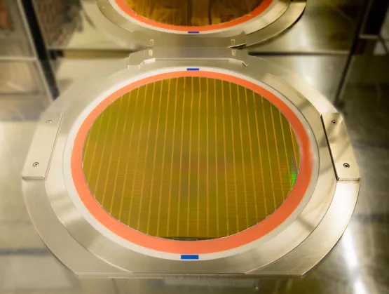
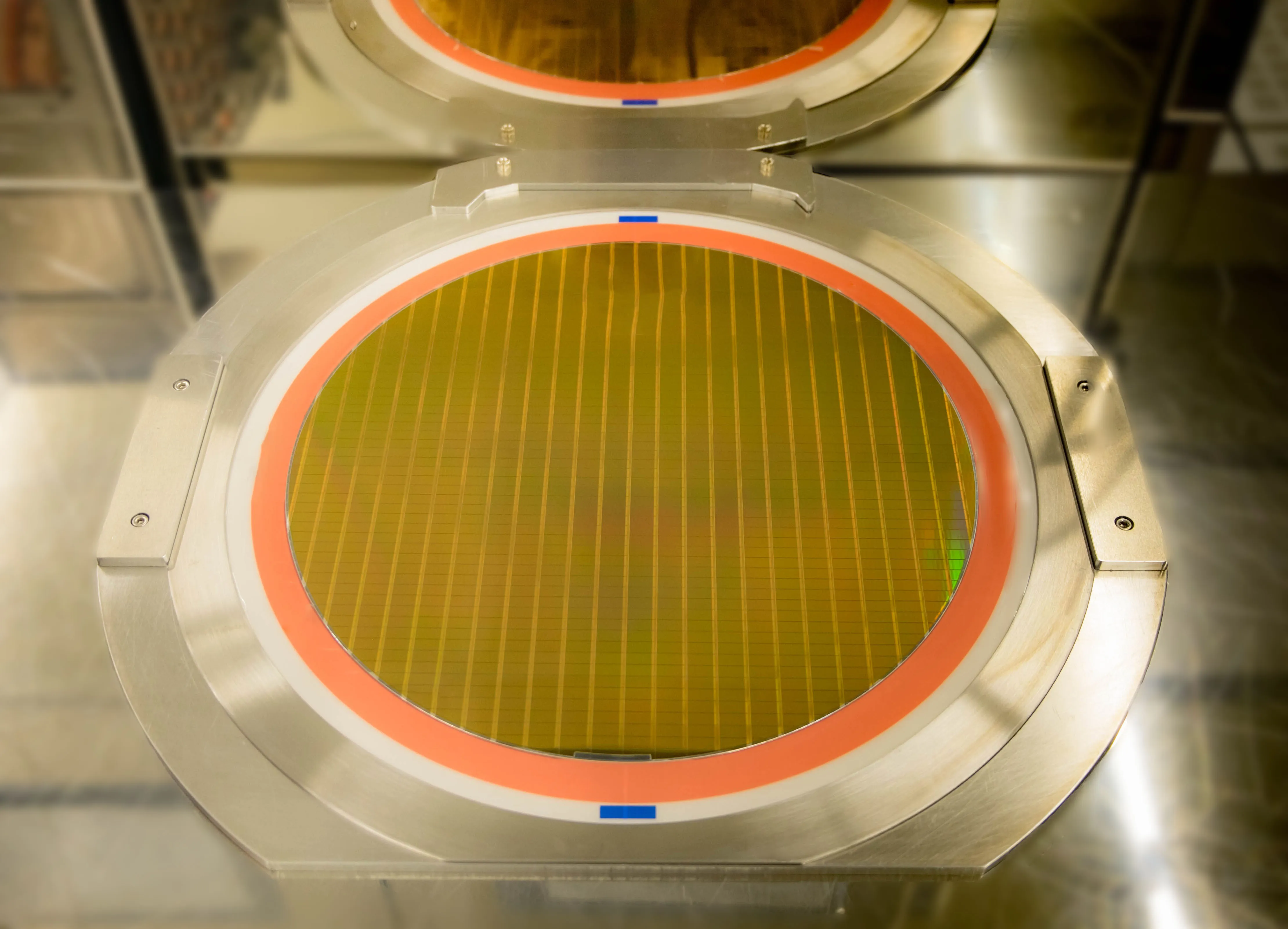
ST Fellow Dr. Andreia Cathelin gave a terrific presentation at the recent CMP Annual Meeting. Now posted and freely available, Performance of Recent Outstanding 28nm FD-SOI Circuits Taped Out Through CMP highlighted eight examples – though she told ASN that she had easily over 50 from which to choose.CMP is a Multi-Project Wafer (MPW) service organization in ICs, Photonic ICs and MEMS. They’ve been organizing prototyping and low volume production in cooperation with foundries for over 37 years. In partnership with ST since 1994, in the fall of 2012 they opened access to MPW runs in the 28nm FD-SOI process. More than 180 tape-outs have been fabricated since then using the process.As Dr. Cathelin said, this lets ST show their industrial clients just how good the technology is. The chips she chose to cover in her presentation get “spectacular performance”, she said, especially for low-power or power-sensitive SoCs.Here’s a quick recap of what she presented (some of which she co-authored), followed by some other SOI-related updates from the CMP meeting.8 (of Many) Great ChipsFD-SOI, said Dr. Cathelin, “...is unmatched for cost-sensitive markets requiring digital and Mixed Signal SoC integration and performance.” In the first dozen slides of her presentation, she gave the technical details on the advantages of FD-SOI in analog, RF/millimeter wave, Analog/Mixed-Signal and digital design. If you're a designer, you'll want to check those out.Then she ran through eight great chips – all manufactured by ST on 28nm FD-SOI through CMP's MPW services. Here they are. (You can click on the illustrations to see them in full screen.)1. A digital delay line with coarse/fine tuning through gate/body biasing in 28nm FDSOI [caption id="attachment_11559" align="alignnone" width="768"] (Courtesy: CMP, ST, ISEN)[/caption] This chip was presented at ESSCIRC '16 by a team from ISEN Lille, Professors Andreas Kaiser and Antoine Frappé (you can get the complete paper by I.Sourikopoulos et al on IEEE Xplore – click here.) As noted in the abstract, “Delay controllability has always been the major concern for the reliable implementation of circuits whose purpose is timing.” By leveraging body biasing in FD-SOI, this novel low-power design architecture for 60GHz receivers enables very high bandwidth together with fine-grain wide range delay flexibility, for implementing Delay Feedback Equalizer techniques in the Intermediate Frequency (IF) reception path. The results are state-of-the-art: ultra wide range, linear control, fs/mV sensitivity and energy efficient controllable delay cells. 2. 28FD-SOI Distributed Oscillator at 134 GHz and 202GHz [caption id="attachment_11560" align="alignnone" width="768"] (Courtesy: CMP, ST, ims)[/caption] Presented at RFIC '17 by a team from the IMS Bordeaux lab, Professor Yann Deval and STMicroelectronics, this chip demonstrates the highest oscillation frequency attainable so far at the 28nm node, be it planar bulk or FD-SOI. (Click here to get the full paper by R. Guillaume et al from IEEE Xplore.) As noted in the abstract, solutions on silicon for mmW and sub-mmW applications have been demonstrated for high-speed wireless communications, compact medical and security imaging. The main challenges are for the signal generation at high frequencies, and this implementation demonstrates spectacular oscillation frequencies close to the transistor’s transition frequency (fT). In this chip, they used body bias tuning to optimize the phase noise, demonstrated very low on-wafer variability, and simulation methods that permit measurement prediction precision within 0.1%.3. A 128 kb Single-Bitline 8.4 fJ/bit 90MHz at 0.3V 7T Sense-Amplifier-less SRAM in 28nm FD-SOI [caption id="attachment_11561" align="alignnone" width="768"] (Courtesy: CMP, ST, Lund U.)[/caption] Extremely energy efficient SoCs are key for the IoT era – but SRAM gets very tricky at ultra-low voltages (ULV). Presented at ESSCIRC '16 by B. Mohammadi et al (on IEEE Xplore here) from Professor Joachim Rodrigues' team at the Lund University, this is a 128 kb ULV SRAM, based on a 7T bitcell. The minimum operating voltage VMIN is measured as just 240mV and the retention voltage is as low as 200mV. FD-SOI enabled them to overcome ULV performance and reliability challenges by letting the Lund U.-lead team selectively overdrive the bitline and wordline with a new single-cycle charge-pump. Plus they came up with a new scheme so it doesn't need a sense amplifier, yet delivered 90MHz read speed at 300mV, dissipating 8.4 fJ/bit-access.4. Matched Ultrasound Receiver in 28FDSOI [caption id="attachment_11562" align="alignnone" width="768"] (Courtesy: CMP, ST, Stanford U.)[/caption] Presented at ISSCC '17 (with an extended relative paper at JSSC '17) by M-C Chen et al with Professor Boris Murmann's team at Stanford, the full title of the paper about this chip is A Pixel Pitch-Matched Ultrasound Receiver for 3-D Photoacoustic Imaging With Integrated Delta-Sigma Beamformer in 28-nm UTBB FD-SOI. (Click here to get it on IEEE Xplore.) It's a a proof-of-concept for a big ultrasound receiver: a “pixel pitch-matched readout chip for 3-D photoacoustic (PA) imaging.” PA is “...an emerging medical imaging modality based on optical excitation and acoustic detection.” It's used in studying cancer progression in clinical research, for example. As noted in the paper abstract, “The overall subarray beamforming approach improves the area per channel by 7.4 times and the single-channel SNR by 8 dB compared to prior art with similar delay resolution and power dissipation.” One of the (many) advantages of FD-SOI in this context is for front-end signal conditioning in each pixel. This unique type of pixel pitch-matched architecture implementation is possible only in a 28nm (or less) node of an FD-SOI technology, as it is matched with the pitch sizing needed for the ultrasound transducers in order to generate signals for a 3-D reading.5. SleepTalker - 28nm FDSOI ULV WSN Transmitter: RF-mixed signal-digital SoC [caption id="attachment_11563" align="alignnone" width="768"] (Courtesy: CMP, ST, UCL)[/caption] Presented at VLSI '16 and JSSC '17 by G. de Streel et al from Professor David Bol’s team at Université Catholique de Louvain la Neuve, the full title of the paper about this chip is SleepTalker: A ULV 802.15.4a IR-UWB Transmitter SoC in 28-nm FDSOI Achieving 14 pJ/b at 27 Mb/s With Channel Selection Based on Adaptive FBB and Digitally Programmable Pulse Shaping (get it on IEEE Xplore here). This chip tackles the IoT requirement for sensing functions that can operate in the ULV context. That means creating wireless sensor nodes (WSN) that can be powered on an energy harvesting power budget – and that's a real challenge if you want to incorporate an RF component that can handle medium data rates (5-30 Mb/s) for vision or large distributed WSN networks. The energy efficiency has to be better than 100 pJ/b. To get there, the UCL-lead team used wide-range on-chip adaptive forward back biasing for “...threshold voltage reduction, PVT compensation, and tuning of both the carrier frequency and the output power. [...] Operated at 0.55 V, it achieves a record energy efficiency of 14 pJ/b for the transmitter (TX) alone and 24 pJ/b for the complete SoC with embedded power management. The TX SoC occupies a core area of 0.93 mm2.”6. A 128x8 Massive MIMO Precoder-Detector in 28FDSOI [caption id="attachment_11564" align="alignnone" width="768"] (Courtesy: CMP, ST, Lund U.)[/caption] This massive MIMO chip was presented at ISSCC '17 by a team from Professors Liang Liu and Ove Edforss at the Lund University in a paper entitled 3.6 A 60pJ/b 300Mb/s 128×8 Massive MIMO precoder-detector in 28nm FD-SOI (H. Prabhu, et al; get it from IEEEE Xplore here). While Massive MIMO (MaMi) will be needed for next-gen communications, it can't be achieved by just scaling MIMO – that would be too costly in terms of flexibility, area and power. As noted in the Lund U. team's intro, “Algorithm optimizations and a highly flexible framework were evaluated on real measured channels. Extensive hardware time multiplexing lowered area cost, and leveraging on flexible FD-SOI body bias and clock gating resulted in an energy efficiency of 6.56nJ/QRD and 60pJ/b at 300Mb/s detection rate.”7. ENVISION: A 0.26-to-10TOPS/W Subword-Parallel Dynamic-Voltage-Accuracy-Frequency-Scalable Convolutional Neural Network Processor in 28nm FDSOI [caption id="attachment_11565" align="alignnone" width="768"] (Courtesy: CMP, ST, KU Leuven)[/caption] Today's solutions for always-on visual recognition apps are an order of magnitude too power hungry for wearables. Running at 10's to several 1OO's of GOPS/W, they use classification algorithms called ConvNets, or Convolutional Neural Networks (CNN). The paper about this chip was presented at ISSCC '17 by a team from professor Marian Verhelst at Katoliek Universiteit Leuven (B. Moons, et al, get it from IEEE Xplore here), and it changes everything. Leveraging FD-SOI and body-biasing, the KU Leuven team solved the power challenge with, “...the concept of hierarchical recognition processing, combined with the Envision platform: an energy-scalable ConvNet processor achieving efficiencies up to 10TOPS/W, while maintaining recognition rate and throughput. Envision hereby enables always-on visual recognition in wearable devices.”8. Fine-Grained AVS in 28nm FDSOI Processor SoC 
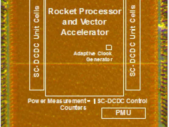
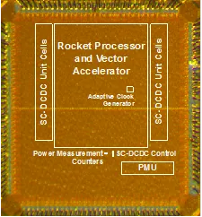
[caption id="attachment_11566" align="alignnone" width="768"] (Courtesy: CMP, ST, UC Berkeley)[/caption] As we learned at SOI Consortium FD-SOI Tutorial Day in SiValley last year, Professor Borivoje “Bora” Nikolic of UC Berkeley is known as one of the world's top experts in body-biasing for digital logic (he and his team have designed more than ten chips in ST’s 28nm FD-SOI!) They presented the RISC-V chip here at ESSCIRC '16 and JSSC '17, in a paper entitled Sub-microsecond adaptive voltage scaling in a 28nm FD-SOI processor SoC (B.Keller, et al, on IEEE Xplore here). As they noted in the intro, a major challenge for mobile and IoT devices is that their workloads are highly variable, but they operate under very tight power budgets. If you apply adaptive voltage scaling (AVS), you can improve energy efficiency by scaling the voltage to match the workload. But in the current gen of SoCs, the AVS timescales of hundreds of microseconds is too slow. The chip the Berkeley team presented brought that down to sub-microseconds by aggressively applying body-biasing throughout the chip, including to workload measurement circuits and integrated power management units. The result is “... extremely fine-grained ( 1μs) adaptive voltage scaling for mobile devices.” (BTW, they expand on some of the details in another paper published in 2017.) These design techniques are now taught at UC Berkeley, as this kind of implementation is the subject of a course in SoC design (including the RF part of transceivers); a first educational chip has already been taped-out and successfully measured. (BTW, Professor Nikolic will once again join Dr. Cathelin and other luminaries in teaching at the SOI Consortium's FD-SOI Training Day in Silicon Valley, 27 April 2018 - click here for sign-up information.)More SOI Through CMPAt the meeting, CMP also made a presentation on all their MPW offerings – you can get it here. On ST's SOI (in addition to 28nm FD-SOI, of course), that includes the new 160nm SOIBCD8s: Bipolar-CMOS-DMOS Smart Power (for automotive sensor interface ICs, 3D ultrasound, MEMS micro-mirror drivers); and 130nm H9-SOI-FEM: Front-End Module (for radio receiver/transceiver, cellular, WiFi, and automotive keyless systems).CMP also provides tutorials that are used by institutions across the globe. A new update to the tutorial, RTL to GDS Digital Design Flow in 28nm FD-SOI Process is now available – you can see the presentation they did about that here. (It now includes LVS and DRC steps with Mentor/Calibre or Cadence/PVS.) Other services, like the 2-day, hands-on THINGS2DO FD-SOI training days at the end of March are always fully booked almost immediately, but don't hesitate to inquire, as they'll be adding more. For some more examples of 28nm FD-SOI chips run through CMP over the years, see their website pages on Examples of Manufactured ICs. There are also some nice examples on pages 21 and 23 of their most recent annual report. For those in the photonics world, CMP has teamed up with Leti to offer Si-310 PHMP2M, a 200mm CMOS SOI platform. CMP is cooperating with Tyndall for the photonics packaging – see that presentation here. Training kits and tutorials will be available in Q3 of this year. And in partnership with MEMSCAP, CMP offers Multi-User MEMS Processes (aka MUMPs) for SOI-MEMS.So lots of terrific SOI resources for CMP – check it out!~ ~ ~Note: special thanks to Andreia Cathelin of ST and Kholdoun Torki of CMP for their help on this piece.
Read More
They've got initial silicon of Dream Chips' ADAS SoC fabbed in GlobalFoundries' 22FDX (FD-SOI) technology, and it's got record power efficiency (read the full press release here). The chip offers high performance image acquisition and processing capabilities and supports AI / Neural Network (NN) vision operation with a total of 1 TOPS at 500 MHz on 4 parallel engines. With all functions including quad-core Arm® Cortex®-A53, Tensilica DSPs, and INVECAS’ LPDDR4-Interfaces activated, the SoC shows single digit power dissipation without the need for forced cooling, which is of significant importance for embedding in automotive environments. [caption id="attachment_11538" align="alignleft" width="277"] Courtesy: Dream Chips Technologies[/caption] Targeting automotive computer vision applications, the SoC was created in close cooperation with Arm, ArterisIP, Cadence, GF, and INVECAS as part of the European Commission’s ENIAC THINGS2DO reference development platform, where about 40 partners in Europe cooperated to propel the FDSOI-Design Ecosystem. Of particular importance is the new and reduced power footprint of this SoC in 22FDX-technology from GF. AI/NN-operation for image recognition is available today, but most of the solutions need active cooling. Implementation of Dream Chip Technologies’ SoC on GF’s 22FDX platform demonstrated single digit Watt and cooling targets for designers managing power dissipation. If needed, the SoC bears the potential to increase the performance even further up to 2 TOPS at 1.0 GHz by applying GLOBALFOUNDRIES’s forward body-bias capabilities and other optimization techniques. The jointly developed ADAS SoC platform from Dream Chip Technologies is available now. Part of GF’s FDXcelerator™ Partner Program, Dream Chip is the largest independent German Design Service company specialized in the development of large ASICs, FPGAs, embedded software and systems with a strong application focus on automotive vision systems (ADAS).
Read More
The solar energy sector shined in a global renewable energy market that maintained steady growth last year despite the United States’ stunning withdrawal from the Paris Agreement. Solar panel costs dropped to an all-time low, driving global demand that surpassed the 100GW mark for the first time on the strength of standout annual 26 percent growth.In 2016, Taiwan began to redouble its transition to renewable energy, most notably phasing out nuclear power as the region increases its reliance on climate-friendly energy sources and seeks more foreign investment, moves it hopes will also boost economic growth and create more jobs.With its land space constraints, the region is fertile ground for rooftop photovoltaic system (PV) systems. So the Taiwan government laid out on ambitious plan to achieve 3,000MW of installed capacity by 2020 – enough to supply electricity for 1 million households while improving air quality, help spruce up the urban landscape and generate jobs.The SEMI Taiwan Energy Group fully backs the government renewable-energy policy. Earlier this year, the group gathered more than 200 industry professionals and government officials to explore challenges and opportunities in deploying more rooftop PV systems. Here are key takeaways from the conference.Infrastructure Reliability Key to High Return on InvestmentSize, reliability and safety are touchstones of rooftop PV system design. To make the best use of space, reduce the cost per kWh, and ensure a long-term, stable supply of electric energy, the PC modules must be: Compact to fit within limited rooftop space Robust to endure extreme temperatures over long periods; resist fire, salt and water damage; and ensure safe, reliable operation Financial Institutions Play Important RoleIn response to the government energy policy, domestic financial institutions have funded select projects or issued bonds and derivative products to support the development of Taiwan’s renewables industry. A key part of these efforts is to evaluate risks in areas such as system module safety, technology and design maturity, energy-generating efficiency and maintenance costs.Circular Economy = Green WorldEnergy storage systems are maturing rapidly to support expanding markets for renewable energy products. Demand for renewable energy systems for homes is growing, fueled in part by low prices, and the adoption of electric vehicles continues to rise as advances in energy storage technology drive down costs and enable longer ranges. At the current pace of technology development, the world could be using 100 percent renewable energy as soon as 2025. However, a pollution-free environment will only be possible with the development of a circular economy – one that regenerates and reuses energy resources. To that end, the SEMI Taiwan Energy Group this year will transform the 11-year-old PV Taiwan exhibition into Energy Taiwan, Taiwan’s largest international platform for facilitating communication and collaboration of the entire renewable energy ecosystem. Exhibition themes will range from solar energy, wind energy, hydrogen energy and fuel cells to green transportation, smart energy storage and green finance. The event reflects the consolidation of the SEMI Taiwan Energy Group’s growing resources and its commitment to a circular economy free of fossil fuels.Emmy Yi is a senior marketing specialist at SEMI Taiwan.
Read More
Smart speakers and voice assistants are already a big part of everyday life for many of us. Improvement in speech recognition accuracy obtained from advancements in natural language processing, machine learning and cloud computing technologies is driving the success of voice assistants. We’re asking Siri to play music, Alexa to order kitchen supplies and OK, Google for the weather. The world’s largest consumer electronics tradeshow, CES, was monopolized by voice assistants this year.But what’s behind the smart speakers? Even smarter microphones. There are two different kinds of tiny microphones in our smart devices, including smartphones, smart home products and smart speakers – capacitive and piezoelectric MEMS (microelectro-mechanical systems) microphones. MEMS microphones offer high signal-to-noise-ratio (SNR), low power consumption, good sensitivity, and are available in very small packages that are compatible with surface mount assembly processes, according to EDN Network. Capacitive MEMS microphones have been the industry standard for 50 years, until recently. A new player hit the scene in the last couple of years – the piezoelectric MEMS microphone.Piezoelectric MEMS microphones are transforming the capabilities of smart speakers by offering better far-field performance, ruggedness and extreme durability over time. In fact, piezoelectric MEMS mics from Boston-based Vesper Technologies, for example, are natively immune to environmental contaminants such as dust, water, humidity, oil and even beer. Piezoelectric MEMS microphones offer significant power savings over battery-powered smart speakers compared to capacitive-based “always on, always listening” solutions. That means that the microphone is absorbing virtually no power until it’s turned on by a “wake word” such as “Hey Siri.”Another crucial advantage of piezoelectric MEMS comes from the inherent linearity of piezoelectric transduction that can withstand extreme sound pressure levels without saturating the microphones. What this means to smart speakers is that the audio quality, particularly the bass response, on the speakers need not be compromised to avoid saturation of microphones in music barge-in scenario. From a consumer perspective, this feature translates to higher wake-word detection accuracy without compromising on audio quality while playing music at loud volume levels. All of these advantages when integrated into microphone arrays lead to improved speech recognition accuracy and consistent long-term performance, a rare combination we think is best achieved with piezoelectric microphones.These different types of sensors can significantly increase the utility rates of smart speaker products in a household, a major challenge that smart speaker developers are trying to solve. Imagine a smart speaker that can interact and move along with you to teach yoga or an Echo Dot in your bedroom that can seamlessly communicate the temperature and/or humidity level to a thermostat without any user interaction. While motion sensors can help create an emotional bond with the user, environmental sensors on-device can offload some of the communication to the cloud or another IoT hub, thereby reducing the latency and power consumption. Some of these features are currently only limited to highly priced niche products, but one can expect the proliferation of these devices into the mass market in the years to come.Amazon’s first-mover advantage resulted in its large market share within the smart speaker segment. Alexa Voice Services’ growing third-party integrations and rapidly evolving ecosystem of connected smart home services indicate a strong foothold for Amazon. Information plays a key role in the race for marketshare in these connected services, and MEMS/sensors are at the forefront of this information-gathering process. Adoption of a wide variety of sensors, including technologies such as piezoelectric MEMS sensors, can provide significant value and competitive advantage in data science.Matt Crowley is CEO of Boston, MA-based Vesper Technologies
Read More