downloadGroupGroupnoun_press release_995423_000000 copyGroupnoun_Feed_96767_000000Group 19noun_pictures_1817522_000000Member company iconResource item iconStore item iconGroup 19Group 19noun_Photo_2085192_000000 Copynoun_presentation_2096081_000000Group 19Group Copy 7noun_webinar_692730_000000Path
Skip to main content
Testifying before a U.S. interagency panel weighing trade tariffs against China, Jonathan Davis, global vice president of industry advocacy at SEMI, yesterday called for the removal of more than 100 products from the list of tariffs proposed by the Trump administration, stressing that an escalation of the U.S.-Sino dispute could trigger a full-blown trade war and hasten deep, unintended damage including higher consumer prices, an expanded U.S. trade deficit, and a slowdown in U.S. economic growth.Representing the electronics manufacturing supply chain, Davis threw the industry’s weight behind protections for valuable intellectual property but argued that “if implemented as proposed, these tariffs will potentially cost tens of millions annually in additional taxes and lost revenue owing to reduced exports, threaten thousands of high-paying U.S. jobs, and not solve U.S. concerns with China.” Davis said the undue harm will ultimately undercut the ability of U.S. chipmakers to sell overseas, stifling innovation and curbing U.S. technological leadership.In testimony at the hearing before the government panel that included representatives from the U.S. Trade Representative (USTR), Departments of Treasury, Commerce, State and Defense, and the Council of Economic Advisers, Davis explained that more than 100 lines – products defined for the purpose of setting import duties – of the proposed tariffs would hamstring the semiconductor supply chain. The tariff lines include fundamental components of the semiconductor manufacturing process that are oxygen for the chip industry. As part of his testimony, Davis also submitted comments on the impact of the tariffs.Charles Gray, general counsel at Teradyne, who also testified at the hearing, said the tariffs will threaten growth while penalizing U.S. companies with supply chains that touch China. Gray and Davis were among more than 100 industry leaders who provided more than 3,000 comments in the May 15-17 hearing to evaluate the impact and efficacy of the proposed tariffs.The hearing followed the Trump administration’s heated, longstanding criticism of China for what it considers unfair trade practices, focusing specifically on intellectual property violations. In recent months, the administration has begun implementing trade actions against China that will increase tariffs, restrict cross-border investment, and introduce significant uncertainty for U.S. businesses.The Section 301 investigation that determined China’s forced transfer of technology and intellectual property discriminated against U.S. firms prompted a proposed 25 percent tariff on $50 billion in U.S. imports from China – a punitive measure that would squarely hit the semiconductor manufacturing industry.SEMI continues to educate policymakers on the deep damage tariffs would exact on the long-term health of the semiconductor industry and the critical importance of balanced trade to the future of the semiconductor industry.For more information on trade or how to participate in SEMI’s public policy program, please contact Jay Chittooran, SEMI public policy manager, at [email protected].
Read More
Broad Global U.S. Electronic Supply Chain GrowthThe first quarter of this year was very strong globally, with growth across the entire electronics supply chain. Although Chart 1 is based on preliminary data, every electronics sector expanded – with many in double digits. The U.S. dollar-denominated growth estimates in Chart 1 have effectively been amplified by about 5 percent by exchange rates (as stronger non-dollar currencies were consolidated to weaker U.S. dollars), but the first quarter global rates are very impressive nonetheless. U.S. growth was also good (Chart 2) with Quarter 1 2018 total electronics equipment shipments up 7.2 percent over the same period last year. Since all the Chart 2 values are based on domestic (US$) sales, there is no growth amplification due to exchange rates.We expect continued growth in Quarter 2 but not at the robust pace as the first quarter.Chip Foundry Growth ResumesTaiwan-listed companies report their monthly revenues on a timely basis – about 10 days after month end. We track a composite of 14 Taiwan Stock Exchange listed chip foundries to maintain a “pulse” of this industry (Chart 3).Chip foundry sales have been a leading indicator for global semiconductor and semiconductor capital equipment shipments. After dropping to near zero in mid-2017, foundry growth is now rebounding.Chart 4 compares 3/12 (3-month) growth rates of global semiconductor and semiconductor equipment sales to chip foundry sales. The foundry 3/12 has historically led semiconductors and SEMI equipment and is pointing to a coming cyclical upturn. It will be interesting to see how China’s semiconductor industry buildup impacts this historical foundry leading indicator’s performance. Passive Component Shortages and Price IncreasesPassive component availability and pricing are currently major issues. Per Chart 5, Quarter 1 2018 passive component revenues increased almost 25 percent over the same period last year. Inadequate component supplies are hampering many board assemblers with no short-term relief in sight.Peeking into the FutureLooking forward, the global purchasing managers index (a broad leading indicator) has moderated but is still well in growth territory.The world business outlook remains positive but requires continuous watching!Walt Custer of Custer Consulting Group is an analyst focused on the global electronics industry.
Read More
Here’s why the embedded community should care whether the chips they use are built on FD-SOI. FD-SOI has “…dramatically improved the landscape for power efficiency,” NXP VP Joe Yu explains in a recent Embedded Systems Engineering piece (you can read it here). He gets into the hows and whys of the i.MX7ULP chip design, taking a deep dive into the things that the embedded folks really care about. He details how FD-SOI decreases leakage and dynamic power, including the roles played by forward and reverse body biasing. He then goes on to explain why it’s better for analog, and how it prevents latch-up. FD-SOI enables new features, too, he points out, like ultra-low power consumption and deep sleep suspend. And perhaps most importantly, he explains how bursty high-performance and ultra energy efficiency are dynamically traded off on an as-needed basis. “Engineers no longer face a forced selection: low-power processor or high-performance processor,” he say. “Rather, the selection for performance or power efficiency can be made instantaneously, as needed, without having to reconfigure.” All of this plus the rich graphics and user interface FD-SOI enables makes the i.MX 7ULP perfect for “…IoT edge devices, as well as smart home controls, building automation, portable patient monitoring, wearables, and portable scanners.” This is an excellent read: highly recommended. Of course, ASN covered the i.mX7ULP when it was first announced (on Samsung's 28nm FD-SOI) last year – you can still read our coverage here. But it’s good to see the company explaining to their customers how FD-SOI will change the way they build products. BTW, you can get all the i.MX7ULP product details on the NXP website here. NXP has also put together a nifty video on the i.MX7ULP – see it here.
Read More
Do you email your doctor when you have a tickle in your throat? Wear a fitness tracker or use an app to monitor your sugar levels, exercise or nutrition? If so, congratulations! You are a part of the rapid growth of digital medicine.Since you’re on the leading edge of this trend to enhance the efficiency of healthcare delivery, you might enjoy learning more about how the medical industry is transforming healthcare in this collection of podcast episodes and video. These are my top picks and just the tip of the proverbial iceberg in how modern medicine is taking today’s technology and applying it to best practices for remote patient monitoring, medical diagnosis, rural healthcare and more.Enjoy! And let me know if you find any others worth the listen!1. Inside Angle: 3M Health Information Systems - Telemedicine: Enhancing Access to Improve OutcomesAccess to healthcare can be a matter of life or death. For some patients, this may mean taking a day off work and driving for hours because services are not available in their hometown.Inside Angle host Dr. Gordon Moore interviews Barb Johnston, co-founder and CEO of HealthLinkNow, about the implementation of telemedicine programs. They discuss how technology impacts telemedicine adoption and related regulations and benefits clinicians and patients in the telepsychiatry and mental health industry. 2. NPR’s The Salt: What’s On Your Plate – This Chef Lost 50 Pounds and Reversed Prediabetes With A Digital ProgramThis short audio clip and article dives into lifestyle and wellness apps designed to motivate users to eat healthier, exercise more and – in some cases – save them from a preventable disease, like diabetes.Wellness apps like Omada Health rely on smartphones, e-coaching, electronic nudging and other methods to encourage users to make and, more importantly, stick to changes that can improve their health. And it’s catching on as other organizations, such as The Centers for Disease Control and Prevention, recognize the difference lifestyle-change programs designed to prevent diabetes are making. 3. Red Hot Healthcare: Episode 57 - Bluer Skies for TelemedicineLast year alone, venture capitalists poured $7 billion into telemedicine. As an emerging concept, telemedicine has a long road ahead until it’s fully integrated and adopted into modern medical practices. Nathaniel Lacktman, partner and health care lawyer with Foley Lardner LLP, discusses legal issues and hurdles surrounding telemedicine today with Red Hot Healthcare host Dr. Steve Ambrose.Lacktman pointed to healthcare providers such as Mercy Virtual Care Center, Mayo Clinic and MDLive that are likely to lead the telemedicine race. This podcast episode is a great listen for entrepreneurs and medical professionals who are interested in learning about compliance and business considerations for the implementation of telemedicine. 4. Digital Health Today: Episode 56 – Eren Bali on Building the World’s Largest Connected Care NetworkEren Bali, CEO and co-founder of Carbon Health, is out to change our fragmented traditional healthcare system with his aim to build the world’s largest connected care network.For Bali, it all started with his sister’s experience consolidating his mother’s health records – scattered over 20 different systems. And from that challenge, his idea to create a universal network that aggregates patient medical records was born.Bali and Digital Health Today host Dan Kendall discuss Bali’s launch of Carbon Health, the new medical records system’s first implementation in a San Francisco primary care clinic, and how providers and patients can get on board with this model. 5. Digital Health Today: Episode 58 – Brennan Spiegel Gets Real About Virtual RealityThis episode of Digital Health Today centers on how Virtual Reality (VR) is being used to enhance patient care. Host Dan Kendall speaks with Dr. Brennan Spiegel, Director of Health Services Research at Cedars-Sinai Health System and Professor of Medicine and Public Health at UCLA, about how immersive technology like VR and Augmented Reality (AR) can improve patients’ experience as well as alleviate pain, anxiety, depression, addiction and more. In a particularly interesting segment, Dr. Spiegel calls the hospital a biopsychosocial jail cell and underscores its importance in not just treating physical ailments but, more wholistically, also addressing the psychological and social wellbeing of patients. 6. TED2017: Raj Panjabi – No one should die because they live too far from a doctor What do you do when access to a doctor means rowing a boat for hours? Millions of people around the world lack access to health care because they live in a remote town or village.In this TED talk, Raj Panjabi, physician in the Division of Global Health Equity at Harvard Medical School, Brigham and Women’s Hospital, and co-founder of Last Mile Health, offers a solution to the problem of healthcare access in the form of the Community Health Academy, a global platform to train and connect community health workers by leveraging devices like smartphones to bring preventative healthcare to even the most far-flung regions of the world. 7. GeekWire’s Health Tech Podcast: How AI is making humans the ‘fundamental thing in the internet of things’Can AI predict which patients are at risk for chronic diseases using their old medical records? This episode of Health Tech Podcast dives deep into the future of healthcare with a look at the potential for AI -- “augmented intelligence” or “assistive intelligence” – to improve patient outcomes, the focus of Ankur Teredesai, a data scientist at the University of Washington and co-founder and CTO of health AI startup KenSci.Clare McGrane, host of GeekWire’s Health Tech Podcast, speaks with numerous experts in this field. They compare precision health to a modern car constantly monitored by microprocessors. The minute something is wrong, you get a warning to take the car to a shop to resolve the issue. The same concept can be applied to humans and deliver big healthcare impacts as research in AI and machine learning continues to evolve. 8. NPR’s Shots: Can Home Health Visits Help Keep People Out Of The ER?In Washington D.C., the city with the highest per capita 911 call volume in all of the U.S., Mary’s Center is piloting a program to provide primary care telemedicine to patients who cannot, or in some cases, do not want to visit the clinic. NPR covers the story of Medicaid patient Dennis Lebron Dolman, who is currently receiving a mix of home visits and virtual treatment.Besides providing healthcare access to rural regions, telemedicine has the potential to reduce emergency room visits in cities as well as improve the health of patients in the long run. Learn more at SEMICON West’s Smart MedTech TechXPOT on Digital Medicine and Remote Patient Monitoring. Hosted by NBMC on July 12, 2018, from 10:30 AM to 12:30 PM, the event will feature healthcare industry leaders exploring state-of-the-art healthcare practices and the future of medical technology. Registration is now open!Amy Ly is a Technical Programs Marketing Coordinator at SEMI.
Read More
Good news: there are far fewer bigoted extremists out there when it comes to FD-SOI vs. FinFETs. People want the best technology for their application. It's that simple. That's a key piece of news from the updated survey by Dan Hutcheson, CEO of VLSI Research, which he presented in the afternoon session of the SOI Consortium's 2018 SOI Symposium in Silicon Valley The afternoon then featured presentations by foundry partners, which I'll cover here. Also in the afternoon were presentations by wafer-maker Simgui, some innovative start-ups leveraging FD-SOI for custom SoCs and the final panel discussion. I'll cover those in Part 3 of this series. BTW, if somehow you missed my coverage of the morning sessions about very cool new products and projects from NXP, Sony, Audi, Airbus and Andes Technology, be sure to click here to read it. The presentations are starting to be posted on the SOI Consortium Events page – but some won't be. Either way, I'll cover them here. VLSI Research A couple years ago at the annual SOI Symposium in Silicon Valley, Dan Hutcheson presented results of a survey he did (ASN covered it – you can still read about it here). At the 2018 event, he presented an update, which is now posted. You can get it here. The FD-SOI roadmap and IP availability are no longer issues for decision makers, he found. The 14nm branch – do you go FinFET or FD-SOI? – is gone. “Fins and FD are complementary,” he observed. Most people said they'd consider using both and running two roadmaps, choosing whichever technology is appropriate to a given design. [caption id="attachment_11841" align="alignnone" width="1000"] (Courtesy: VLSI Research, SOI Consortium)[/caption] From a transistor viewpoint, the top reasons to choose FD-SOI is that it's better for analog and has lower leakage/parastics. It's perceived as better for complex, high mixed-signal SoCs, and especially for RF and sensor integration. In fact, people see RF as the new mixed-signal, wherein FD-SOI is uniquely positioned for 5G and mmWave. From a business viewpoint, FD-SOI is perceived to have real advantages. In particular, FD-SOI wins when it comes to keeping down design costs, manufacturing costs and time-to-market. IoT is still the hottest target market for FD-SOI, to which he adds high growth expected in automotive and medical. Samsung With 20 tape-outs in 2018, Samsung is seeing an acceleration in its FD-SOI business. “The trend is healthy,” said Hong Hoa, SVP of the company's foundry business. FD-SOI, he continued, is on a “differentiation path.” Samsung's 28nm FD-SOI process, called 28FDS is at full maturity with very strong yields. They're seeing more customers and a wider range of applications. The design infrastructure, silicon-verified IP and methodologies are also all mature. They have optimal implementation and verification guidelines for body bias design, a body bias memory usage guide, and a body bias generator integration guide. The process supports Grade 1 automotive, and will be qualified for Grade 2 in a few weeks. FD-SOI, Hoa reminded the audience, offers superior RF performance compared to both planar bulk and 14nm FinFET. The Samsung strategy is to first provide a base for for the FD-SOI process, then add RF and eMRAM. The base for 28nm was done in 2016; they added RF in 2017 and eMRAM this year. The Samsung platform for IoT applications integrates both RF and eMRAM to support multi-function needs in a single platform. Lead customers are already working with eMRAM in their designs, he added. (BTW, Samsung has a really nice video explaining their eMRAM offering – you can see it on YouTube here.) The basic PDK for the Samsung 18nm FD-SOI process (18FDS) will be available in September 2018, with full production slated for fall of 2019. It will deliver a 24% increase in performance, a 38% decrease in power, and a 35% decrease in area for logic. RF for the 18FDSplatform will be ready by the end of this year, and eMRAM beginning in 2019. GlobalFoundries With design wins from 36 customers underway, 12 of which are taping out in 22FDX (GF's 22nm FD-SOI process) this year, the market has validated FDX for differentiation, said GF SVP Dr. Bami Bastani. And indeed, designers are using it for a wide array of applications across North America, Europe, Asia/Pacific and Japan. Customers in the North America are designing in 22FDX for NB-IoT, industrial, RF/analog, mobile, network switches and cryptocurrency applications. In Europe, it's more or less the same plus automotive/mmWave, optical transmission, wireless BTS and AI/ML. In Asia Pacific/Japan the mix is similar to Europe. Bastani sees the three big enablers as the the strengths of the roadmap, the ecosystem and multi-sourcing from Dresden and Chengdu (where they're already equipping the cleanrooms). He also tipped his hat in acknowledgment to the partnership with FD-SOI wafer supplier Soitec, noting that they have gone the extra mile to match GF's requirements. So that was the first part of a great afternoon. As mentioned above, my next post (part 3) will cover a very informative presentation by wafer-maker Simgui on the markets in China, plus talks by some innovative start-ups leveraging FD-SOI for custom SoCs and the final panel discussion.
Read More
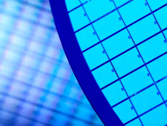
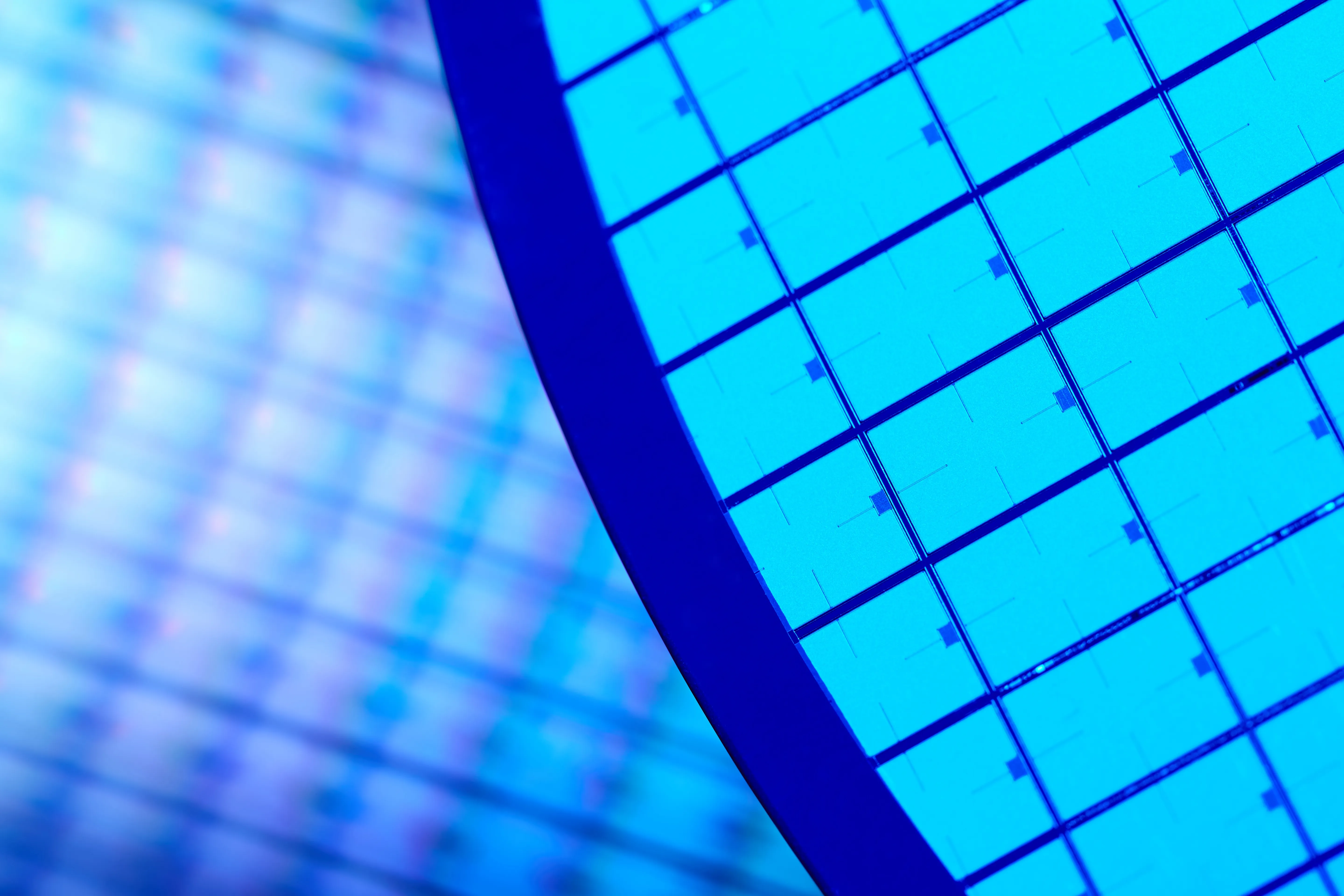
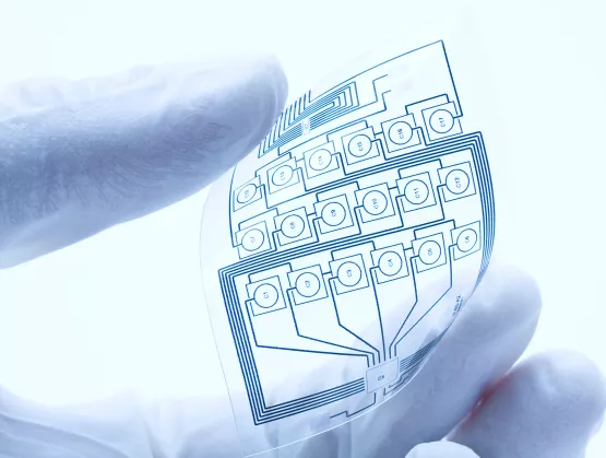
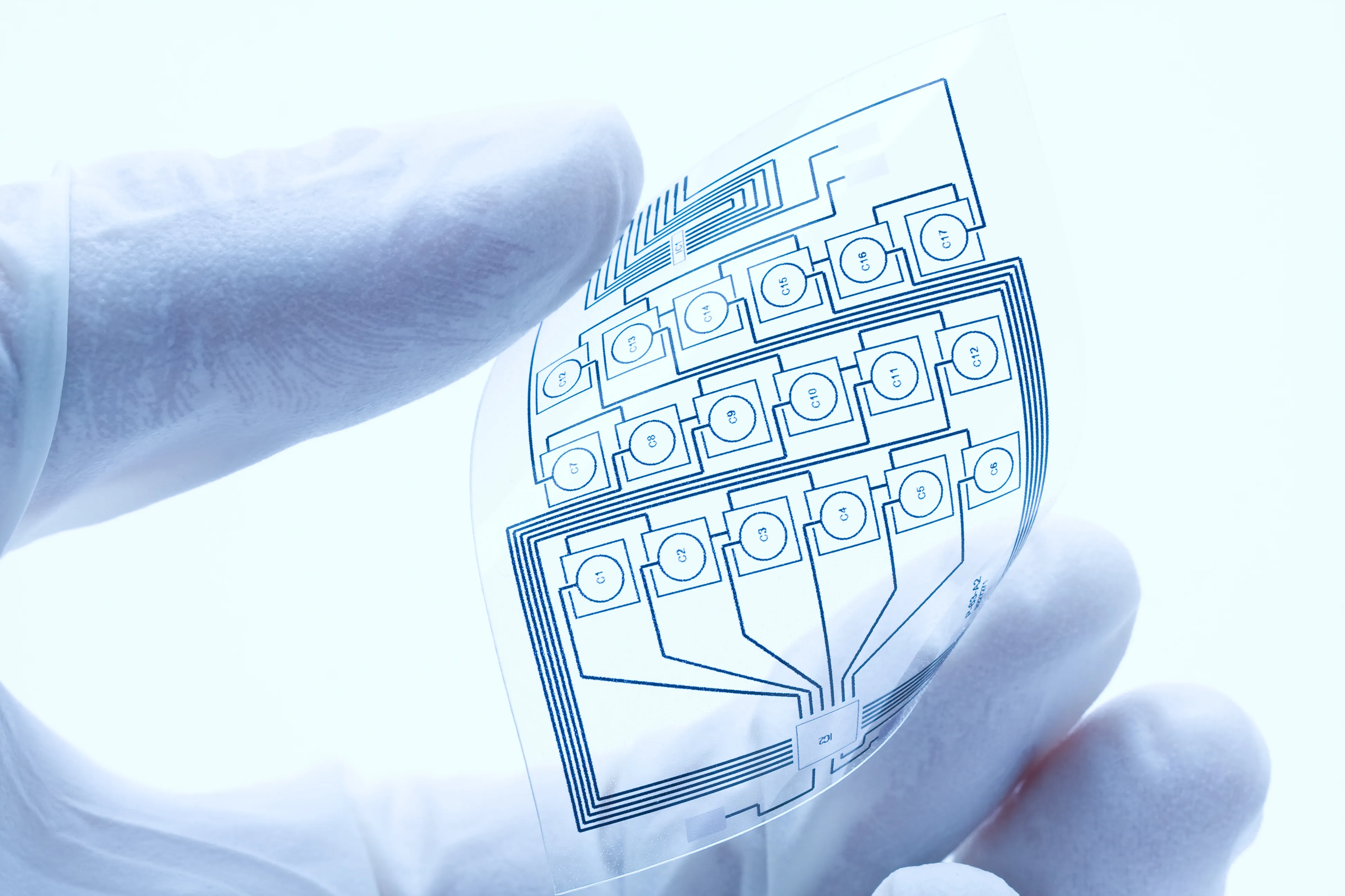
The growth of China’s semiconductor industry outstripped sector expansion in many other regions in 2017 thanks in part to heavy government investments and supportive state policies. But China’s chip industry also struggled under the weight of overheated investment, inconsistent project quality, insufficient investment in research and development, a poor ability to innovate, and barriers to international cooperation. To overcome these headwinds to growth, China must identify global trends in the development of global semiconductor industry and better understand the forces it needs to mobilize to further expand its own semiconductor sector. AI and 5G fuel global semiconductor industry growthIn 2017, global semiconductor industry revenue reached a seven-year peak, expanding 22 percent to nearly USD 420 billion, and entered a new growth phase with artificial intelligence (AI), 5G and other new technologies leading the surge with greater market segmentation, diversification and decentralization. The emergence of smart automobiles, smart cities, smart medicine, AR/VR and other new markets headed the list of new applications. In the next three to five years, semiconductor industry growth is expected to remain stable, with no marked declines. In 2018, the growth rate is expected to fall to between 5 percent and 8 percent, with the expansion more comprehensive and balanced. The memory market, in particular, will find it hard to match its 2017 blistering growth rate. The market’s expected growth of 10 percent to 20 percent will be chiefly driven by DRAM and 3D NAND Flash. In 2019, NAND growth will continue but DRAM shipments could decline. Emphasis on both innovation and investment key to sustainable growth of Chinese IC Under the China government’s Guidelines to Promote National IC Industry Development, designed to provide key policy guidance and capital support for the development of China’s IC industry, the Chinese semiconductor industry is seeing particularly rapid growth that is expected to be a key contributor to continuing global industry expansion. In IC design, HiSilicon and Unigroup Spreadtrum RDA ranked among the top 10 in the world. In wafer fabrication, Chinese IC manufacturing accounted for 13 percent to 15 percent of global market capacity despite SMIC and Huahong Group lagging international competition in advanced processing. In packaging and testing – China’s strongest segment – JCET, NFME and Huatian Technology also ranked in the global top 10. The Guidelines to Promote National IC Industry Development has fueled a boom in capital investments. However, investments must go well beyond fab construction to add new capacity for China’s semiconductor industry to flourish. A strategy for sustainable, long-term chip industry growth must focus more on technology innovation while continuing heavy capital investments, though it takes time for innovation to lead to higher capacity demand and GPD growth and more jobs. Despite large investments by the 02 Special Project in semiconductor equipment and materials, China trails other regions of the world in advanced technologies. Global spending on semiconductor equipment reached a record-breaking USD 56 billion in 2017, with Korea a major driver. In 2017, Samsung alone invested USD 25 billion in semiconductor equipment, followed by TSMC (USD 10.8 billion), Intel (USD 11.5 billion), Hynix (USD 8.5 billion), Micron (USD 0.5 billion), SMIC (USD 2.3 billion) and YMTC (USD 2 billion). In 2018, Samsung’s equipment spending is expected to drop slightly, to USD 24 billion, while investments by Intel and TSMC will be remain roughly equal. China’s equipment spending will continue to grow in 2018, with SMIC and YMTC maintaining investment levels similar to last year’s and other China semiconductor manufacturers starting to ramp up investments. In 2018, China is expected to surpass Taiwan in equipment spending to claim the number two position after Korea. SIIP China dedicated to international connection and cooperation The huge investments in China’s semiconductor industry need to be supported by robust business strategies, greater international cooperation, deeper expertise in advanced technologies, and more skilled workers. China lags the global industry in all of these areas. The rapid rise of China’s semiconductor industry has raised concerns among many countries over China’s growing influence, with some, most notably the United States, going so far as to implement containment measures. Other regions including Japan, Korea and Taiwan followed suit. The continued growth of China’s semiconductor industry hinges on technological innovation enabled by international cooperation, as well as strong international communication to allay concerns and misunderstandings over the rising prominence of China’s chip sector. China must overcome these obstacles. One partial solution is for China to convince the rest of the world that its need a thriving semiconductor industry if only to meet enormous demand for electronics products within its own borders. As the largest international semiconductor industry association, SEMI enjoys a unique ability to strengthen the connection between China’s semiconductor sector and its international counterparts. SEMI is well-known for its vital support of the traditional semiconductor equipment and materials markets, but SEMI’s work also spans IC design, manufacturing, packaging and testing. What’s more, SEMI has expanded into innovative market vertical applications such as AI, smart manufacturing, smart transportation and smart automotive as it aims to bring together supply chains across these growth areas. For its part, SEMI China remains dedicated to improving communications and cooperation between the Chinese and global semiconductor industries. SEMI China will also continue to encourage deeper collaboration among individual enterprises and government institutions in the interest of industry growth while making full use of SEMI’s international, professional and localization platform to promote the development of China’s semiconductor industry. Last year, we established SEMI Innovation Investment Platform (SIIP) China to help grow China’s pool of skilled workers, promote advanced technology, generate industry capital, and expand China’s semiconductor industry while developing stronger connections with chip sectors in other regions. SIIP China is focused on the following: Promoting sustainable development of the Chinese semiconductor industry Establishing stronger connections to help take advantage of global technology and investment opportunities Providing a platform for open communications between the Chinese and global semiconductor industries Promoting greater coordination between China and its global partners Helping newly enterprises secure funds for expansion Encouraging greater cooperation with foreign semiconductor manufacturers in the interest of openness and mutual benefit will be the best way for China to overcome obstacles to the development of its semiconductor industry. Meanwhile, China will continue to strive to merge into the global semiconductor industry and become a key partner. SEMICON China has witnessed the development of Chinese semiconductor industry SEMICON China marked its 30th anniversary this year. Over the past three decades, China’s semiconductor industry has seen remarkable growth. This year’s SEMICON China was the largest ever. SEMICON China and FPD China 2018 numbered 3,628 booths, covered 74,000 square meters of exhibition space and attracted 1,116 exhibitors from 21 countries and regions and 91,252 professional attendees from 58 countries and regions. Most of China’s top device makers and global leading packaging houses, together with their equipment and materials suppliers, exhibited at SEMICON China and FPD China 2018, representing the global IC manufacturing ecosystem. The number of SEMICON China and FPD China 2018 visitors jumped 32.3 percent from last year, with representation by professionals from the design, manufacturing, assembly and test, equipment and materials sectors. Lung Chu is President of SEMI China.
Read More
Thanks to you and the more than 5,000 other industry experts who contribute your time and brainpower, the SEMI Standards Program is celebrating its 45th anniversary in 2018. The first SEMI Standards meeting was held in 1973 to create a dimensional specification for silicon wafers. At the time, the proliferation of more than 2,000 different wafer specifications had led to major inefficiencies as the industry was just getting underway. To address this problem, wafer suppliers gathered under the auspices of SEMI and quickly developed consensus specifications for 2-inch wafers, and by the mid-1970s over 80 percent of wafers being shipped conformed to the new standard.Since that time, the SEMI Standards Program has expanded both geographically and technically. The program now has 20 technical committees in China, Europe, Japan, Korea, North America, and Taiwan, tackling manufacturing challenges across the electronics supply chain. Critical milestones include the development of SEMI S2, the comprehensive safety guideline that has drastically reduced industry incidents and continues to be updated to keep up with the hazards associated with semiconductor manufacturing, and the SECS/GEM and EDA suites of equipment communication standards, which are the backbone of modern day semiconductor “Smart Manufacturing.”As we commemorate our 45th year, there has never been a more diverse and active agenda as we look to solving issues in new areas such as Fan-Out Panel Level Packaging, Electron Microscopy Workflow, and flexible hybrid electronics. Of course, the Standards Program owes its success and longevity to you. I am repeatedly amazed by the dedication of Standards Members, and look forward to continuing the industry collaboration – together we can make the next 45 years as fun and productive as the first!As SEMI president and CEO Ajit Manocha has stated, “SEMI Standards is the oxygen of the industry.”SEMI Standards has saved the industry untold billions of dollars by defining interoperability specifications, guidelines and test methods that have streamlined semiconductor manufacturing and ensured the smooth operation of hundreds of pieces of equipment – all working automatically 24X7.What's more, SEMI Standards has enabled the production of more than 2.2 billion wafers and 1.8 trillion IC devices. Referenced more than 10 million times in production fab purchases, more than 25 SEMI Standards, on average, are cited in each purchase order for semiconductor equipment and materials in the electronic manufacturing ecosystem.
Read More
Can it be that no more new semiconductor fabs are being built in the U.S.?The last new volume fab known is Micron’s Building 60 in Utah, according to the SEMI World Fab Forecast report published in February 2018. The catch is Building 60 is not a new or greenfield facility but rather an existing structure being retooled for 3D NAND. Fab equipment spending for this fab is expected to be high in 2018.Then there is Fab 42 from Intel. Construction started in 2011 before it was shelved. It is expected to begin equipping by end of this year, with equipment spending expected to be high next year.Other fabs built many years ago are still ramping such as Globalfoundries Fab 8 phase 3 (TDC) and D1X (module 1 and module 2). D1X is a research and development pilot, not a high-volume fab. And Globalfoundries’ plans for a second fab in Malta have been pushed out.Samsung in Austin has space for more modules, but there is no indication they will ever be added.The SEMI World Fab Forecast shows five smaller facilities either planned or under construction, but these have little impact in this U.S. fab construction trend.And that’s basically it! No more volume fabs!If we divide fab equipment spending into two categories – investment in new capacity versus upgrades – we see a declining trend for fabs adding capacity. See chart below. (Compare 2005-2011 with 2017-2019). If we look at 2017, 2018 and 2019, Globalfoundries, Intel, and Micron are the big investors in new capacity.This year 60 percent of all fabs are expected to invest in equipment to add capacity, but just one or two volume fabs (Micron and Globalfoundries) account for the bulk of this growth. Same story for 2019, with two volume fabs (Intel and Globalfoundries) representing the lion’s share of the growth. Strike the Intel and Globalfoundries fabs from the equation, and investments in additional capacity would fall below upgrade spending levels.Once these fabs have reached full capacity, additional equipment investments will significantly lag spending increases for upgrades, signaling the end of new fabs in the U.S.
Read More
Peel-and-stick simplicity isn’t just for adhesive bandages any more. IoT and flexible hybrid electronics (FHE) are bound to change hardware business models. And flexible displays will breathe life into any surface.These were among the insights foreshadowing the future of the FHE, electronic textiles, IoT, MEMS and sensors industries at the FLEX Japan and MEMS Sensors Forum Japan 2018. At the April event, organized by SEMI-FlexTech-MSIG, nearly 200 attendees shared their observations and lessons learned in the development of processes, products and applications. Presentations and discussions revealed these five takeaways.1. Expect the unexpected with FHE developmentFlexible Hybrid Electronics (FHE) continues to shrink the size and weight of products, enabling new markets and concepts. “FHE takes printed electronics and adds ICs for getting performance out of the PE structure,” said Wilfried Bair of NextFlex, adding that “peel- and-stick electronic products are one example of unexpected new markets enabled by FHE capabilities.” One potential application is large peel-and-stick safety sensors adhered to buildings to warn of structural dangers.Another surprising turn: With new insights into OLED technology originally developed for flexible displays, Cambridge Display Technology (CDT) has devised an innovative medical diagnostic tool for markets such as biomedical and agricultural monitoring. The tool features an atmosphere-processable OLED component with a simplified OLED structure encapsulated in aluminum foil.2. IoT and FHE devices should change hardware business modelsThis is the standard business model for many new FHE products: develop a product, manufacture it, find customers and sell. FHE and IOT device developers were encouraged by Jam Kahn of Gemalto to consider flipping the script: During FHE product development, explore building an after-market revenue stream by controlling and mining the data for trends it reveals. Because of its data harvesting potential, IoT is an excellent emerging technology for this strategy.The “Experience Economy” could create 200 connectable items per person, generating strong revenue streams from the collection and analysis of massive amounts of sensor-generated data. The key is for the data to be actionable. That means hardware suppliers must extend their focus to software development. “A recent study of California investors found that by 2025, 60 percent of global business profits will be from data,“ noted Harri Kopola of VTT, who advised hardware producers to examine business models that produce continuous value by leveraging software. “With FHE, we are creating the path to digitization for non-digital industries, and these industries need complete solutions,” he said.Hardware provider Xenoma, for example, sells an electronic shirt with sensors for measuring muscle movements, heart rate and other health-related data. Xenoma’s Ichiro Amimori said the company offers its open-source software development kit for free under one condition: The developer must share the collection data with Xenoma. The idea is that the more data collected, the greater Xenoma’s ability to improve human health over the long term and achieve its long-term vision of alleviating disease.3. Roll-to-roll and sheet-to-sheet manufacturing will meet in the middleOne of the big advantages of flexible and printed electronics was its promise to enable the manufacturing of electronics on a roll-to-roll (R2R) process in atmospheric (or close) conditions, like newspaper, rather than one sheet at a time, as with displays or wafers. But as development of inks and interconnects progressed, along with the placement of discrete and thinned-die components and basic flexible substrates on a moving web, most research and development (R D) and limited-production runs moved to sheet-fed systems to control material costs for experiments and low-volume production. R D on printing electronics processes split into two camps: the simple printed components camp on R2R, and the camp backing more flexible hybrid electronics development on a sheet-by-sheet basis. But progress didn’t stop.Harri Kopola of VTT highlighted new R2R inspection and test capabilities in the VTT pilot line in Finland. R2R processing advances incorporate ideas from biology, chemistry, optics, optoelectronics, advanced inspection and test capability, illustrating the multidisciplinary nature of FHE. While accurate, high-speed, pick and place of thinned, bare die remains the domain of sheet-to-sheet manufacturing, look for more improvements in accuracy and speed.Another new manufacturing concept that turns business models on their heads – “minimal fabs” – focuses on creating limited-run equipment and processes that use 3D printing and do not require cleanrooms. With a relatively low cost of entry, the approach enables electronics to be produced affordably anywhere.4. Powering the IoT is a grand challengeThe requirement for edge devices to function without intervention for long periods raises hard questions about how to power the devices. Using organic photovoltaics (OPV) in textiles to harvest energy from light could be one solution, according to Kasimaesttro Sugino of the Suminoe Textile Technical Center. ULVAC’s answer to the IoT power issue are requirements for edge device micro-batteries to be environmentally benign, safe, flexible and compatible with semiconductor processing less than .1 mm in height. The micro-batteries must also feature a long life and support continuous power output, high power density, low self-discharge (over 10 years) and mass production, said Shunsuke Sasaki of ULVAC. The batteries are being built on silicon, glass and stainless steel with dry, thin-film vacuum processing. 5. Flexible displays bring any surface to lifeWith their durability, flexibility, low-cost processing and programmability, flexible displays can transform any surface into a content-rich display with messages that make lives healthier, simpler and safer.One example is FlexEnable’s organic thin-film transistor (OTFT), a device made possible not only by recent advances such as the ability to build organic material transistors on plastic and the increasing clarity of new film materials but by continuous manufacturing process improvements. These advances are improving switching times and the color and video capabilities of thin-film transistors while retaining their flexibility, low power consumption and communication capabilities. Simon Jone of FlexEnable gave the examples of wrapping a display around the blind spots of automobiles or replacing side-view mirrors with interior monitors showing feeds from an external camera, approaches that would improve safety while reducing wind drag and increasing fuel efficiency.E Ink’s reflective technology and flexible products are coming to market with a wider color spectrum. The company’s Michael McCreary said its designers are specifying the panels for innovative projects such as the exterior walls of the San Diego International Airport parking garage. Used to communicate with airport visitors, the installation is weather-proof, programmable and self-powered.
Read More
The MEMS industry has huge growth potential. Will MEMS fabrication act as a bottleneck to continued expansion or a critical conduit to achieving that potential? Slow development cycles, multiple fabrication platforms and high cost for small R D volumes are barriers to rapid development of new products. Understanding the special features of MEMS fabrication — with its many ecosystem options — will help your company to navigate successfully these challenges as you more quickly develop new and unique products.The sheer diversity and varying requirements of MEMS devices and the one product, one process approach are the root causes of most MEMS fabrication challenges. While a single approach will not suit all companies, forming an ecosystem that leverages different companies’ expertise is one of the best ways to address these challenges. However, knitting together this ecosystem is difficult because having multiple partners in the mix only works if the entire supply chain follows common basic design rules and a common top-level technology development roadmap.Because establishing these commonalities takes time and effort, many large- and medium-sized companies prefer to own their supply chain, regardless of the costs. In contrast, emerging companies that cannot support heavy capital investments in new equipment will inevitably find foundries that have all the equipment in place — as well as a wide variety of MEMS processes — a more attractive option. As you embark on a MEMS fabrication journey, which options should you consider to stay ahead of the pack?Finding ecosystem partnersSince there are so many different technology choices that make process integration difficult in MEMS fabrication, technology know-how is the key to developing unique products in time. If you are not able to own your supply chain, you must find ecosystem partners whose expertise both matches and complements your technology (Table 1). Table 1: Ecosystem options as a function of company expertise. 1=Excellent fit 2=Good fit 3= Ok fitYou must also understand how your company can add value — either directly to the end-product or to the other partners in the ecosystem. Above all, there must be trust among partners. A lack of mutual trust will lead to inadequate information-sharing and cumulative knowledge-gathering — slowing problem-solving and/or causing excessively long development cycles. Option 1: Own your supply chainWhile few companies can support Option 1 — having the whole supply chain in-house (like Bosch or STMicroelectronics) — the benefits are many: all know-how will be contained within the company, IP is easy to protect, and supply-chain management is simpler. However, this model demands a significant investment in tools and, in the long run, substantial effort and money to remain technologically competitive in each part of the supply chain.Option 2: Outsource the ASICYou might opt for a fully owned supply chain — outsourcing only ASIC fabrication and possibly ASIC design and assembly. This option requires significant expertise in MEMS technology, freeing you from the limitations of a fabless operation model as you gain more control of MEMS fabrication processes. It also offers more IP protection than you would have with a foundry.While the disadvantages of Option 2 are similar to the fully owned supply chain model, you can mitigate them by outsourcing part of the MEMS chip fabrication supply chain or outsourcing some development to wafer supply companies that can handle the customer-designed embedded structures inside the wafer and/or multi-stack wafer packages. Outsourcing will shorten the process flow and reduce the amount of capital required for growth. A third outsourcing option is to farm out especially difficult or incompatible steps, delivering multiple benefits such as access to better materials, including specialized polymers – which are typically more expensive than silicon – and precious metals, such as gold or platinum, which can contaminate equipment during thin-film deposition processes.Options 3-4: Foundry modelsWhile more companies still own the whole supply chain or outsource the ASIC portion of their device than use MEMS foundries, the MEMS foundry solution is still an especially good option for cost-conscious companies. If you cannot afford the substantial investment needed for new tools and/or advanced materials or your product requires rapid scaling-up because of short lifecycles, you should explore foundry solutions. There are two main types: pure-play foundries (Option 3) and a foundry with design services and its own IP (Option 4). Option 3 offers no design services, nor does it provide its own designs. It is an excellent choice for a MEMS design-based company lacking its own MEMS fabrication line. However, if your company lacks in-depth knowledge of MEMS design, Option 4 will give you design support and possibly some IP as well. Option 5: Buy the MEMSOption 5 is to buy ready-made MEMS chips and use them as the foundation to build your component. This is solid choice if your company is high in the value chain or has system-level expertise.In the future, MEMs ecosystem players will win by offering both design-library development and a supporting portfolio of MEMS process design kits — just as the IC industry now does. This winning approach will significantly shorten the MEMS product-design cycle – from idea to process development and finished product – and will ultimately change the rules of the game for the MEMS fabrication industry.Based in Vantaa, Finland, D.Sc.(Tech.) Heikki Holmberg develops new business opportunities for Okmetic’s high-performance silicon wafers. He also manages Okmetic’s research portfolio, including European Union- and nationally funded research projects. For more information, visit: https://www.okmetic.com/
Read More