downloadGroupGroupnoun_press release_995423_000000 copyGroupnoun_Feed_96767_000000Group 19noun_pictures_1817522_000000Member company iconResource item iconStore item iconGroup 19Group 19noun_Photo_2085192_000000 Copynoun_presentation_2096081_000000Group 19Group Copy 7noun_webinar_692730_000000Path
Skip to main content
Default Banner Image

Lara Chamness

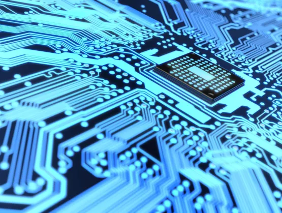
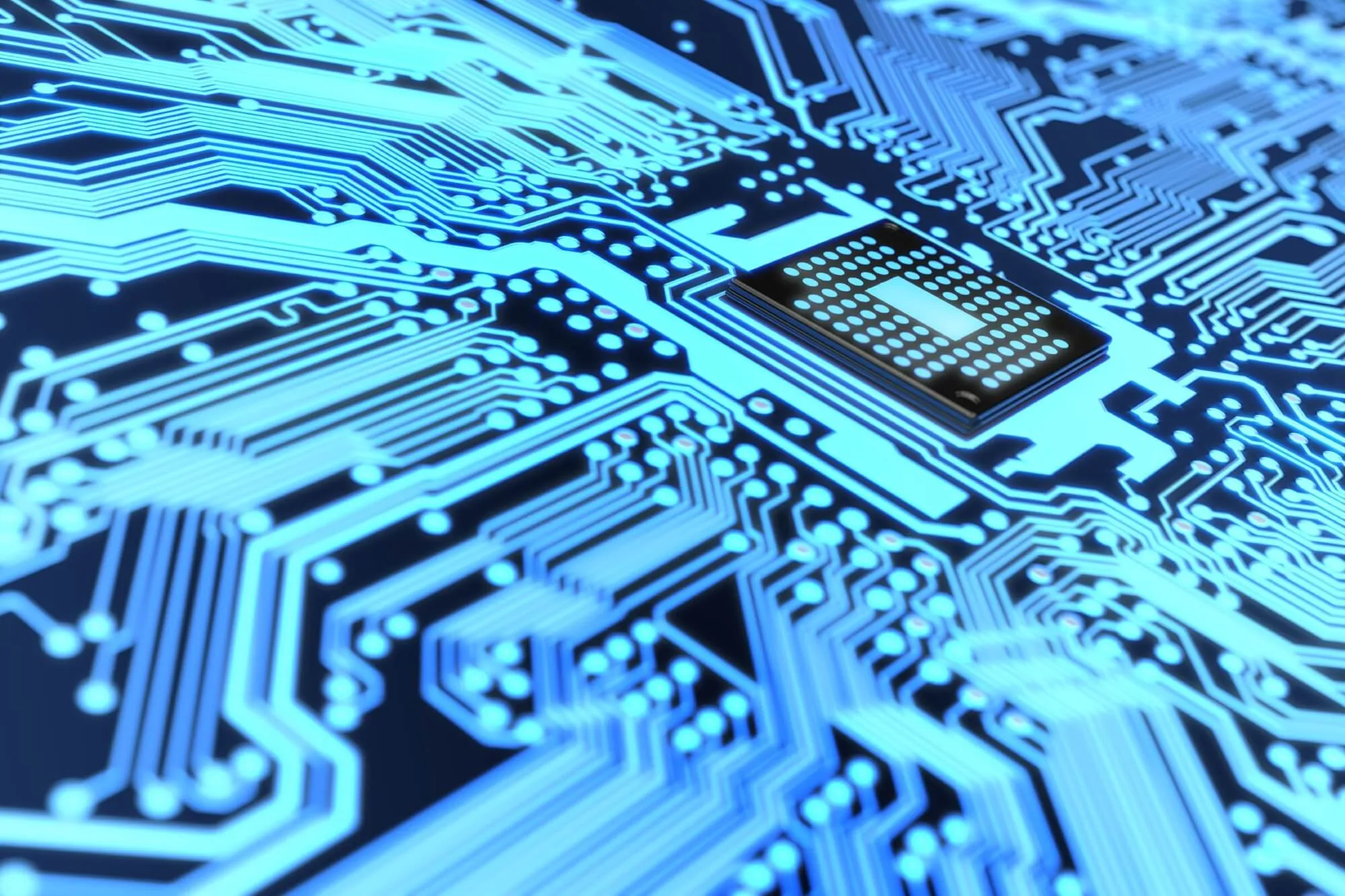
This is an exciting year to be in the semiconductor industry: semiconductor-related companies are trading at all-time highs and most expect record device shipments and revenues as well as equipment revenues. This growth is primarily fueled by demand drivers such as Automotive Electronics, Medical Electronics, Mobile Phones, and Industrial Electronics. With this recent growth spurt and the proliferation of end-market applications that consume ever increasing numbers of semiconductors, it is tempting to conclude that the industry has seen the end of cycles.At the annual SEMI/Gartner, Bulls Bears Industry Outlook symposium, Stifel’s Patrick Ho, asserted that “Gone are the days of your grandfather's cycles.” Robert Marie of Semiconductor Advisors, maintained that “Cycle shape has changed due to demand drivers, consolidation, maturation and other factors.”However, Gartner’s Bob Johnson was quick to assert, “Whenever people say that cycles are over and that the industry is going to grow forever ─ the industry is at a peak.” He noted that Gartner expects semiconductor revenues to surpass $400 billion this year, increase two percent next year, but decline in 2019. He indicated that Memory is driving this year’s market expansion but will drag down market growth next year as pricing gains achieved will be lost beginning in the fourth quarter of this year. The softness in 2018 is expected to have a detrimental impact on the industry’s spending plans. Gartner predicts that capital spending will shrink to just under one percent next year and contract 7 percent in 2019.In addition to softer memory pricing in the near term, Gartner does not anticipate that China will invest significant amounts until 2020/2021. SEMI on the other hand is currently modeling an increase of 9 percent in fab equipment expenditures in 2018, which is largely driven by China. China is expected to have an even greater impact on global fab capital expenditures, claiming the top position in 2019, according to SEMI.Looking at demand drivers, more specifically the “Internet of Things”, it is clear that the explosion of connected “things” is fundamentally reshaping our industry. The fragmented nature of these markets require niche applications and device architectures with the majority of these devices being commoditized MEMS and other solid-state sensors. Growing market revenue does not necessarily translate into industry profitability as the declining average selling price.So how can the industry benefit from all of this connectivity? Dr. Sam Wang from Gartner discussed how the Internet of Things has made AI practical, and how artificial intelligence brings out the value of IoT. He noted that AI: Drives the demand for advanced wafer process technologies Encourages the adoption of HMC, HBM, eDRAM, ReRAM, PCM, STT-MRAM, memristors processing in memory Incorporates ADC within sensors and computing in sensors Increases the use of 2.5D, 3D, TSV and SiP technologies Enables chip design flow optimization in EDA Fuels the need of new ATE testers for testing complex AI chips Prompts more start-ups and M A opportunities The overwhelming majority of semiconductor devices used in IoT are commodities, creating a renaissance for smaller wafer diameter fabs (200mm and smaller; see related 200mm article). The value of the IoT will come from the ecosystem that supports it, such as data centers and networks that enable connectivity. There are also opportunities for the adoption of new processor technologies, as Gartner’s Werner Goertz pointed out. He stated that the current processors used in IoT processing were designed for very different use cases, and that conditions are now ripe for a disruptive processor supply chain to optimize edge-based AI.2017 is indeed going to be a great year for the semiconductor industry: device average selling prices have improved dramatically, device manufacturers are investing in new capacity, while stock prices of suppliers throughout the supply chain are trading at elevated levels. 2018 is anticipated by many industry pundits to be another growth year, albeit at more conservative growth levels. Although the Internet of Things literally offers the industry billions of applications, its full impact on the industry remains to be seen. And we’ll definitely keep a close eye on developments in China.For SEMI market research, visit www.semi.org/en/MarketInfo
Read More
SEMI reported that worldwide sales of new semiconductor manufacturing equipment are projected to increase 19.8 percent to total $49.4 billion in 2017, marking the first time that the semiconductor equipment market has exceeded the market high of $47.7 billion set in 2000. In 2018, 7.7 percent growth is expected, resulting in another record-breaking year ─ totaling $53.2 billion for the global semiconductor equipment market. The SEMI Mid-year Forecast predicts wafer processing equipment is anticipated to increase 21.7 percent in 2017 to total $39.8 billion. The other front-end segment, which consists of fab facilities equipment, wafer manufacturing, and mask/reticle equipment, will increase 25.6 percent to total $2.3 billion. The assembly and packaging equipment segment is projected to grow by 12.8 percent to $3.4 billion in 2017 while semiconductor test equipment is forecast to increase by 6.4 percent, to a total of $3.9 billion this year. In 2017, South Korea will be the largest equipment market for the first time. After maintaining the top spot for five years, Taiwan will place second, while China will come in third. All regions tracked will experience growth, with the exception of Rest of World (primarily Southeast Asia). South Korea will lead in growth with 68.7 percent, followed by Europe at 58.6 percent, and North America at 16.3 percent. SEMI forecasts that in 2018, equipment sales in China will climb the most, 61.4 percent, to a total of $11.0 billion, following 5.9 percent growth in 2017. In 2018, South Korea, Taiwan, and China are forecast to remain the top three markets, with South Korea maintaining the top spot to total $13.4 billion. China is forecasted to become the second largest market at $11.0 billion, while equipment sales to Taiwan are expected to reach $10.9 billion. The following results are in terms of market size in billions of U.S. dollars: The Equipment Market Data Subscription (EMDS) from SEMI provides comprehensive market data for the global semiconductor equipment market. A subscription includes three reports: the monthly SEMI Billings Report, which offers an early perspective of the trends in the equipment market; the monthly Worldwide Semiconductor Equipment Market Statistics (SEMS), a detailed report of semiconductor equipment bookings and billings for seven regions and over 22 market segments; and the SEMI Mid-year Forecast, which provides an outlook for the semiconductor equipment market. For more information or to subscribe, please contact SEMI customer service at 1.877.746.7788 (toll free in the U.S.). For more information online, visit: https://discover.semi.org/equipment-market-data-registration.html
Read More
Prior to 1997, the industry enjoyed the “mask maker’s holiday” when IC feature sizes were larger than the lithography wavelength and the industry enjoyed the number of transistors per area doubling for no additional cost. This era ended when 248nm lithography was adopted. 248nm lithography enabled device manufacturers to extend traditional optical lithography but forced the adoption of resolution enhancement techniques such optical proximity correction and phase shift masks. 193nm lithography was introduced for 90nm features and the industry was required to adopt increasingly complex strategies to shrink device geometries further such as liquid immersion, double patterning, and more recently multiple patterning. These techniques have enabled device manufacturers to extend traditional optical lithography while next-generation lithography approaches, including extreme ultraviolet (EUV), maskless lithography, and nanoimprint remain in the background.EUV is the most favored next-generation lithography and has received the lion’s share of press and research dollars. EUV was initially scheduled to be used for 65nm feature processing but persistent challenges with this technology remain unsolved. Key obstacles associated with EUV are: finding adequate source power, EUV photoresists, and developing mask manufacturing infrastructure. Significant progress has been made and there are now beta EUV tools in the field. The extended delay of EUV forced chipmakers to extend 193nm immersion lithography with multiple patterning down to sub-10nm. With so much invested in optical lithography, even when EUV is ready, it is expected that chip makers will use a combination of EUV and 193nm immersion with multi-patterning for leading-edge devices.The delay in EUV for volume production has impacted the photomask market. Last month, SEMI reported that the worldwide semiconductor photomask market recorded a record high in 2016, reaching $3.32 billion. SEMI also noted that captive mask suppliers have significantly increased their market share due to the capital intensity required by leading-edge manufacturing.It remains to be seen what lithography solutions the industry will implement to maintain Moore’s law as the costs of advanced lithography increase faster than increased device density gains. What is clear is that the photomask market is mature and that captive shops, with their deep pockets, are assuming an increasingly important role. Still merchant shops continue to serve a vital function by servicing standard mask sets and providing manufacturing capability in the event of a service disruption.A recent SEMI published report, Photomask Characterization Summary, provides details on the 2016 Photomask Market for seven regions of world including North America, Japan, Europe, Taiwan, Korea, China, and Rest of World. The report also includes data for each of these regions from 2003 to 2018 and summarizes lithography developments over the past year.Please click here to download a copy of the SEMI Photomask Market Characterization Executive Summary. For information on all SEMI Market Information, visit: www.semi.org/en/MarketInfo.
Read More