downloadGroupGroupnoun_press release_995423_000000 copyGroupnoun_Feed_96767_000000Group 19noun_pictures_1817522_000000Member company iconResource item iconStore item iconGroup 19Group 19noun_Photo_2085192_000000 Copynoun_presentation_2096081_000000Group 19Group Copy 7noun_webinar_692730_000000Path
Skip to main content
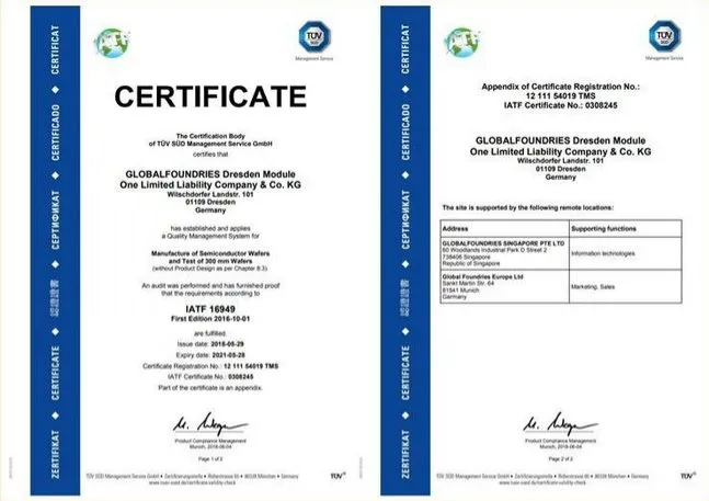
[caption id="attachment_11914" align="alignright" width="150"] Mark Granger, GlobalFoundries' VP Automotive Product Line Management[/caption] GF's 22FDX® (22nm FD-SOI) offering is on an automotive roll. The technology platform has been certified for several key automotive standards, and GF has announced an exciting new ADAS customer in Arbe Robotics. In addition to sharing info from various press releases and blogs, ASN also had a chance to catch up with Mark Granger, GF's VP for automotive, who provided some great insights. Read on! Taking the Heat When it comes to compliance, automotive industry standards are excruciatingly rigorous. Every part that goes into a car must adhere to the relevant standards: chips are no exception. One such standard is the AEC – Q100, a “Failure Mechanism Based Stress Test Qualification For Integrated Circuits”. The AEC – aka the Automotive Electronics Council – handles those testing standards and certification. Grade 2 means a technology is certified for the -40°C to +105°C ambient operating temperature range. To achieve Grade 2 certification, devices have to successfully withstand reliability stress tests for an extended period of time over the specified temperature range. GF recently announced that 22FDX has been AEC Q100 Grade 2 certified (press release here). However Granger adds that for their customers, they've added additional headroom that takes them to 125°C. They're now working on Grade 1 certification, he says, which means the devices are certified to handle junction temperatures up to 125°C (and there again, GF has added additional headroom that takes them to 150°C). That should be done by the end of 2018. The ability you get with FD-SOI to tune the transistors using body biasing is really beneficial here, he says. For GF, the 22FDX qualifications exemplifies their commitment to providing high-performance, high-quality technology solutions for the automotive industry. The automotive industry is driven by a “zero excursions – zero defects” mindset, says Granger, and that drives the foundry, too. SOI has been used for decades across industries where heat and electromagnetic radiation are challenges, bringing soft error rates (SER) down by orders of magnitude, notes Granger. (SOI, btw, essentially eliminates what are known as Single Event Upsets (SEU) caused by latch-up, which in turn brings down SER.) That in turn, ties into the FIT (failure in time) rate – and that's part of the ISO 26262 “Road vehicles – Functional safety” standard – where 22FDX is also certified. As a part of GF's AutoPro™ platform, 22FDX allows customers to easily migrate their automotive microcontrollers and ASSPs to a more advanced technology, while leveraging the significant area, performance and energy efficiency benefits over competing technologies. Moreover, the optimized platform offers high performance RF and mmWave capabilities for automotive radar applications and supports implementation of logic, Flash, non-volatile memory (NVM) in MCUs and high voltage devices to meet the unique requirements of in-vehicle ICs. GF's Fab 1 in Dresden, Germany (which is where they do 22FDX) also has achieved ISO-9001/IATF-16949 certification, which demonstrates that it is capable of meeting the stringent and evolving needs of the automotive industry. (IATF is the International Automotive Task Force. 16949 is a Quality Management System (QMS) certification specifically for the automotive sector.) Granger wrote a really informative blog on the GF website – you can read it here. It includes this graphic, indicating where in the car 22FDX-based parts are expected to go. [caption id="attachment_11913" align="alignleft" width="1000"] Here's how GF sees the applications for 22FDX and other chip technologies in automotive applications. (Courtesy: GlobalFoundries)[/caption] On Radar GF recently announced that Arbe Robotics selected 22FDX® as the process technology for its groundbreaking patented imaging radar. Arbe aims to achieve fully automated system capabilities and enable safer driving experiences for autonomous vehicles (read the press release here). As the first company to demonstrate ultra-high-resolution at a wide field of view, Arbe Robotics’ radar technology can detect pedestrians and obstacles at a range of 300 meters, in any weather and lighting conditions. The processor creates a full 3D shape of the objects and their velocity, and classifies targets using their radar signature. As Granger noted in his blog, “Radar is one of several sensor types used to detect objects near a vehicle, to enable features like adaptive cruise control. Lidar is another. It uses pulsed lasers to determine distance from an object by measuring the time it takes for the light to reflect back. However, lidar is currently expensive and is affected by weather conditions. Radar is less expensive, and higher-resolution radars promise to compete well with lidar in automotive applications, thereby enabling lower-priced vehicles to enjoy greater ADAS capabilities. 22FDX-based radar sensors can provide higher resolutions and less latency than current radar sensors at a very low total system cost.” While they may be complementary at first, there is a battle brewing between high-resolution radar and lidar, Granger told ASN. Putting their solution on 22FDX enables Arbe to achieve a 77 GHz mmWave radar and compete cost-effectively with lidar. “They wanted the best,” says Granger. 22FDX can achieve the requisite Ft and Fmax figures of merit. And with transistor stacking, they can also integrate the power amplifier (PA) on a single device. With the low inherent capacitance of the PA in 22FDX, you can get the high power output you need for mmWave but with low power consumption. GF blogger Dave Lammers has also written a great piece about the Arbe solution (you should read it: here's the link). “The company said its advanced technology allows the detection of small targets, such as a human or a bike even if they are somewhat masked by a large object such as a truck,” he writes. “The imaging radar can determine whether objects are moving, and in what direction, and alert the car in real-time about a risk. “While other car sensors can fail when it is raining, if there’s fog, and due to blinding lights such as a sudden reflection, Arbe’s radar is completely oblivious to all those factors. The custom designed radar processor creates a full real-time 4D image of the environment, and classifies targets using their radar signature.” Avi Bauer, Arbe's VP of R D, is now clearly an SOI fan. Lammers quotes him as saying, “With SOI the design is more straightforward, and (voltage) biasing allows you to do things that cannot be done in standard CMOS. For the transmit and receive modules, SOI’s higher resistivity substrate benefits the passive components – inductors and capacitors – and allows good isolation. High Q passives are important. At 22nm, SOI allows better performance overall.” Clearly good things are coming down the road for FD-SOI!
Read More
The Scaling Technologies TechXPOT at this year’s SEMICON West (Scaling Every Which Way! – Thursday, July 12, 2:00pm-4:00pm) will explore traditional scaling as the industry marches toward 3nm and beyond, as well as technologies that enable 3D architectures, die stacking, and interconnect scaling. The session will also provide an update on how the various players (foundry, IDM, fabless, and application developers) are jockeying for innovation leadership. As a prelude to the event, SEMI asked Priya Mukundhan, director, Technology Development and Applications, at Rudolph Technologies, and a speaker at the TechXPOT, to provide her insights into challenges associated with metrology and inspection.For a full list of speakers and program agenda, visit http://www.semiconwest.org/programs-catalog/scaling-every-which-way. Priya Mukundhan, director, Technology Development and Applications, Rudolph TechnologiesSEMI: What are the key challenges that need to be addressed to provide the kind of metrology and inspection solutions that will be needed by the industry as scaling – in all its forms (e.g., traditional, 3D ICs, interconnect, and different transistor architectures) – is pursued at 5nm and then at 3nm? Priya Mukundhan: With respect to metrology needed to scale FinFETs, the following will be key: Gate critical dimension (CD) at the fin sidewall, gate height, gate profile Fin CD, height and profile Dopant profiles Stress measurement in the fin Composition in thin film and interface These challenges are currently being handled using in-line CD solutions, CD scanning electron microscopy (CD-SEM) and CD atomic force microscopy (CD-AFM), along with optical critical dimension (OCD) measurements. There is no single technology that can take all of these measurements, and determining the right solution is application-dependent[1].Issues associated with inspection and scaling include the following: Bright-field inspection lacks the sensitivity to detect defects smaller than those found at the 20nm node Detecting defects that are 5nm or smaller is achieved using electron beam inspection tools, but these single-electron beam inspection systems are prohibitively slow and cannot meet the high-volume manufacturing (HVM) requirements for defect inspection Buried defects Void detection in 3D SiP structures, front and backside inspection Sidewall crack detection in packaging SEMI: Can you provide a summary of the R D roadmap for metrology/inspection tools that you see emerging in order to get to 3nm? PM: Hybrid metrology is currently in use, especially for CD metrology. To support the development efforts, techniques that provide complementary information as well as those that eliminate uncertainties will be required. Researchers at imec[2] have started exploring technology combinations to gain insight into how new structures function. Some of the findings in imec’s study include the following: The combination of transmission electron microscopy (TEM) and scanning probe microscopy (SPM) provides a unique approach of imaging combined with a functional analysis capability In situ SPM could potentially determine composition (SIMS) as well as functional properties (electrical) Fast Fourier transform scanning spreading resistance microscopy (FFT-SSRM) is a novel technique that measures carrier profiles in semiconductors. This overcomes the current SSRM limitations of signal distortions due to parasitic resistances while measuring on small volumes such as FinFET and nanowires Multi-electron beam inspection can be used for HVM for sensitivity to smaller SEMI: How will metrology and inspection be impacted beyond 3nm? What kinds of tools will be needed by that point in time?PM: There are several different transistor options that have been identified by leading edge wafer fabs and consortia looking beyond the 5nm node roadmap[3,4]. Some of the options on the table include the following: 1) Extension of the current FinFET in the form of gate-all-around FET2) Creating them with new materials by adding ferroelectrics (e.g., negative capacitance FET, or NC-FET) 3) Complementary FET4) Vertical nanowires and nanosheet FETsThese possibilities bring new challenges and require characterization at the material level. Also, the industry as a whole will have to redefine what it means to do composition at the nanometer level. This could be the beginning of a trend towards array-based metrology, i.e., measurements on an array of devices to gather statistically significant data[2].Regarding metrology needs at 3nm, it is too early to determine what kind of tools would be needed only for R D and how many of them would need to be extended to high-volume manufacturing (HVM). From an inspection perspective, there will be a continued migration towards computer aided design (CAD)-based inspection, as well as having the ability to deal with large image data sets (petabyte, big data). Furthermore, inspection algorithms should be improved, along with better staging for better image stitching.References Bunday, E. Solecky, A. Vaid, A. F. Bello, X. Dai, “Metrology capabilities and needs for 7nm and 5nm logic nodes,” Proc. Of SPIE, Vol. 10145, 101450G, pp. 1-41, 2017. Imec roadmap and imec magazine. Intel roadmap. https://semiengineering.com/transistor-options-beyond-3nm/ Debra Vogler, SEMI
Read More
Self-driving cars have been all the rage in both the trade and popular press in recent years. I prefer the term “autonomous vehicles,” which more broadly captures the possibilities, encompassing not only small passenger vehicles but mass transit and industrial vehicles as well. Depending on who’s talking, we will all be riding in fully autonomous vehicles in five to 25 years.The five-year estimates come from startups eager to raise venture capital while the 25-year estimates stem from Tier 1 automotive suppliers who tend to be more conservative in outlook. Regardless of the timeframe, a multitude of investors – national governments, venture capitalists and companies – are dedicating significant capital and effort to make autonomous vehicles a reality.I must admit that I did not fully grasp the enthusiasm for self-driving cars until last year. First, I’ve always enjoyed driving, unless I’m in stop-and-go traffic, so I couldn’t imagine relinquishing the task. Second, I’ve deliberately arranged my life to spend minimal time in my car. However, traffic has become much heavier in my metropolitan area (Boston), and I know that many people in cities around the world face longer commutes and waste more time in gridlock.What is the solution to this problem that is only getting worse? I had an epiphany while walking through Shinigawa Station in Tokyo, one of the busiest train stations in the world. Dense streams of people crisscrossed the station on their individual paths, managing to avoid collisions without the aid of traffic controls. Evidently, humans have an innate collision-avoidance ability that makes traffic controls for pedestrian crowds unnecessary. If autonomous vehicles could achieve the same excellence in collision-avoidance, we could potentially reduce or eliminate traffic controls for vehicular traffic, providing a huge gain in transportation efficiency and relief from gridlock.Sensors as core building blocksNew and improved sensors, many based on micro-electromechanical systems (MEMS) technology, are key to achieving this vision. While MEMS inertial sensors (such as accelerometers and gyros) are already integral to the core safety systems in conventional vehicles, they are also essential to improved self-navigation in autonomous vehicles.The challenge for MEMS suppliers is to deliver inertial sensors that meet the requirements for self-navigation systems, which are different and more demanding than for safety systems.Pinpointing a vehicle’s position requires “dead reckoning” based on inertial sensor signals as a supplement to GPS input. Undesirable drift in the inertial sensor signals due to mechanical quadrature, temperature sensitivity and noise can quickly add up to a large error in position that may result in a collision. To meet the more rigorous requirements for autonomous vehicles, suppliers must design MEMS inertial sensors that are substantially more precise and resistant to drift. This requires design software that is both extremely accurate and fast, as well as increasingly precise and reliable manufacturing capabilities.Other MEMS-based devices, such as micromirrors and micro ultrasound transducers (MUTs), are also promising options for implementing vision and range-finding systems in autonomous vehicles. These sensing systems are needed for building electronic versions of the human collision-avoidance abilities that I witnessed in Shinigawa Station – and it is these systems that autonomous vehicles must emulate.When will self-driving cars become a reality? Aside from the provocative question that got you to read this far, I don’t have a definitive answer. It will undoubtedly occur in phases, ranging from the driver-augmentation systems available in today’s cars to the full autonomy and ubiquity that will allow reduction of traffic controls in 20 years or more. It is clear that the ultimate goals for autonomous vehicles are highly worthwhile, and that achieving those goals will require better-performing and more diverse MEMS sensors. Stephen (Steve) Breit, Ph.D. is Senior Director, MEMS Business, at Coventor, a Lam Research Company. Steve has been responsible for overseeing development and delivery of Coventor’s industry-leading software tools for MEMS design automation since joining Coventor in 2000. Steve holds numerous patents on software systems and methods for MEMS design automation and virtual fabrication. He holds a Ph.D. in Ocean Engineering from MIT and a B.S. in Naval Architecture and Marine Engineering from Webb Institute.For more information, visit: https://www.coventor.com
Read More
The Advanced Lithography TechXPOT at this year’s SEMICON West will explore progress in extreme ultraviolet lithography (EUVL), its economic viability for high-volume manufacturing (HVM) and other lithography solutions that will address the march to 5nm and onward to 3nm.As a prelude to the event, SEMI asked Mary Ann Hockey, director for Advanced Emerging Lithography at Brewer Science Inc., and a speaker at the TechXPOT, for insights into the status of directed self-assembly (DSA) as it applies to the industry’s march to patterning for the 3nm node and beyond. For a full list of speakers and program agenda, visit http://www.semiconwest.org/programs-catalog/lithography-5nm-and-below.Mary Ann Hockey, director for Advanced Emerging Lithography at Brewer Science Inc.SEMI: What is the current status of materials development for DSA?Hockey: We are currently working with strategic customers to implement high-quality DSA chemical material solutions. We are both addressing near-term implementation of standard PS-b-PMMA block copolymers (28-30nm Lo) by leveraging our strategic partnership with Arkema, France, and building a library of high-chi block copolymers for long-term device requirements (Figure 1). SEMI: How do those developments prepare the technology for 5nm, 3nm or beyond?Hockey: We have engaged the strategy of engineering a library of novel high-chi block copolymer (BCP) platforms for next-generation DSA technology requirements of 3-5nm devices. One key objective is a global focus on easing implementation into a manufacturing environment. This objective requires large process windows for guided alignment (accommodating pitch and guide size target variability), minimizing BCP microphase anneal times (short anneal time supports high throughput), and streamlining the total number of process steps required for volume production (Figure 2).SEMI: How will industry’s use of DSA be intertwined with immersion lithography?Hockey: We envision immersion lithography as the foundation enabler with strategic use of optical lithography for generating consistent critical dimension (CD) sizes of DSA guides/templates for low cost of ownership.SEMI: What about the combination of DSA and extreme ultraviolet lithography (EUVL) to fabricate devices at 5nm, 3nm, and beyond?Hockey: EUVL and DSA can potentially work in harmony to support next-generation device technology. DSA can be made with the capability of lithography rectification or enhancing EUVL photoresist sidewalls and targeting low line-edge roughness and line-width roughness (LER/LWR) values.Debra Vogler, SEMI
Read More
Christian G. Dieseldorff, Industry Research Statistics Group, SEMI (June 12, 2018)The semiconductor industry is nearing a third consecutive year of record equipment spending with projected growth of 14 percent (YOY) in 2018 and 9 percent in 2019, a mark that would extend the streak to a historic fourth consecutive growth year, according to the latest update of the World Fab Forecast report published by SEMI. The industry last saw four consecutive years of equipment spending growth in the mid 1990s.Korea and China are leading the growth, with Samsung dominating global spending and ascendant China on a fast, steep rise, surging ahead of all other markets. See figure 1.Figure 1: equipment spending by region (includes new and refurbished)Samsung is expected to reduce equipment investments in 2018. Despite the ebb, the company still accounts for a dominant 70 percent of all investment in Korea. At the same time, SK Hynix is increasing its equipment spending in Korea.China’s equipment spending is forecast to jump a whopping 65 percent in 2018 and 57 percent in 2019. Notably, 58 percent of investments in China in 2018 and 56 percent in 2019 stem from companies with headquarters in other regions such as Intel, SK Hynix, TSMC, Samsung, and GLOBALFOUNDRIES. Domestic, Chinese-owned companies – backed by large government initiatives – are building an impressive number of new fabs that will start equipping in 2018. The companies will double their equipment investments in 2018 and again in 2019.Meanwhile, other regions are also ramping up investments. Japan is beefing up equipment spending by 60 percent in 2018, with the largest increases by Toshiba, Sony, Renesas and Micron.The Europe and Mideastern region will boost investments by 12 percent in 2018, with Intel, GLOBALFOUNDRIES, Infineon and ST Microelectronics as the largest contributors. Southeast Asia will increase investments by more than 30 percent in 2018, although total spending is proportionately smaller than in other regions owing to its size. The main contributors are Micron, Infineon and GLOBALFOUNDRIES, though companies including OSRAM and ams are also increasing investments.The SEMI World Fab Forecast, which also includes information on other companies, covers data and predictions through the end of 2019, including milestones, detailed investments by quarter, product types, technology nodes and capacities down to fab and project level.Learn more about the SEMI fab databases at:www.semi.org/en/MarketInfo/FabDatabase and www.youtube.com/user/SEMImktstats.
Read More
With chipmakers looking toward 5nm manufacturing, it’s clear that traditional scaling is not dead but continuing in combination with other technologies. The industry sees scaling enabled by 3D architectures such as die stacking and the stacking of very small geometry wafers. Interconnect scaling also comes into play. This year’s Scaling Technologies TechXPOT at SEMICON West (Scaling Every Which Way! – Thursday, July 12, 2:00PM-4:00PM) will provide an update on the evolution of scaling and describe how the various players (foundry, IDM, fabless, and application developers) are jockeying for innovation leadership. As a prelude to the event, SEMI asked speakers to provide insights on important scaling trends. For a full list of speakers and program agenda, visit http://www.semiconwest.org/programs-catalog/scaling-every-which-way.Challenges for gate-all-around (GAA) and FinFET devicesDiederik Verkest, imec Distinguished Member of Technical Staff, Semiconductor Technology and Systems“During the processing of GAA devices, there are ‘non-line-of-sight’ hidden features that are difficult to control and characterize and may also lead to new defect mechanisms that would impact yield, and possibly product reliability.”Common performance boosters for gate-all-around (GAA) FETs and FinFETs include lower access resistance, lower parasitic capacitance, and stress. “However, one specific performance booster that only applies to GAA is the reduction of the spacing between the vertical wires or sheets,” says Diederik Verkest, imec distinguished member of technical staff, Semiconductor Technology and Systems. “This reduces parasitic capacitance without affecting drive current and hence benefits both performance and power.” He further notes that imec demonstrated the first stacked gate-all-around (GAA) devices in scaled nodes. “In fact, we are the only ones that published working circuits – ring oscillators in a scaled node using industry-standard processes – in our case replacement metal gate (RMG), and embedded in situ doped source/drain (S/D) epitaxy.”“There are two elements of the stacked GAA architecture that need to be addressed,” says Verkest. “The first is that this architecture uses epitaxially-grown layers of Si and SiGe to define the device channel. The use of grown materials for the channel and the lattice mismatch between the two materials represent a departure from the traditional fabrication of CMOS devices, so the industry needs to develop and gain confidence in novel metrology that allows for good control of the layers and also proves their low defectivity.” The second aspect is the three-dimensional nature of the GAA devices. “During the processing of these devices, we have ‘non-line-of-sight’ hidden features that are difficult to control and characterize and may also lead to new defect mechanisms that would impact yield, and possibly product reliability.”Huiming Bu, Director, Advanced Logic/Memory Research - Integration and Device, IBM Research, Semiconductor Group"A new device architecture beyond FinFET is required to provide a full technology node scaling benefit (i.e., density, power and performance) at 5nm and 3nm.”Huiming Bu, director, Advanced Logic/Memory Research - Integration and Device, IBM Research, Semiconductor Group, says that naming of technology nodes has been used extensively for marketing strategies in “foundry land,” but the designations have lost much of their meaning as technology scaling differentiators. “That said, when it comes to technology innovation and value proposition, IBM, in conjunction with Samsung and GLOBALFOUNDRIES, has developed the GAA NanoSheet transistor for 5nm to provide a full technology node scaling benefit in density, power and performance,” says Bu (Figure 1). The key parameters for intrinsic device optimization when scaling to the 3nm node, explains Bu, are the NanoSheet width for better electrostatic characteristics, and the number of sheets for increased current density. Also necessary are strain engineering for carrier transport enhancement, and interconnect innovations for parasitic RC reduction. “Beyond that, the industry needs to look into something different, something more disruptive.”Figure 1. TEM cross section of stacked NanoSheet transistors. SOURCE: IBM Research Materials challengesMaterials challenges are also a concern as the industry moves to 5nm and below. “We see increasing complexity in the material systems that are being used,” explains Verkest. One example he cites in scaled FinFET or GAA technologies is the use of two to three layers of different materials – typically metals such as TiN – to which small amounts of other elements are added to set device characteristics such as the threshold voltage. “At the same time, the requirements for the thickness of these materials, driven by gate dimensions for example, or the distance between the wires, are increasingly challenging.” Other examples of materials challenges are the use of two to three different types of insulators in the middle-of-the-line, each with different etch contrasts. “We use novel materials such as carbon containing oxides or oxynitrides that have lower dielectric constants in order to boost the performance of circuits,” he says, noting that the materials list “is quite long.”Several critical dimensions in transistors at advanced technology nodes have already reached a few monolayers of atoms, fueling expectations for innovation at the material level for transistor scaling, Bu notes. “The other argument is that there is a growing gap between computing demand and the slowdown of technology advancement driven by conventional scaling,” says Bu. One trend that addresses this gap is integrating more computing functions that make the technology solution more modular, which naturally leads to the incorporation of more materials for more applications. Bu cautions, however, that introducing new materials in semiconductor technology has never been easy. “It takes many years of R D to reach this implementation point, if it ever happens. So, do we need new materials when the industry moves to 5nm and 3nm? Yes, though I expect new material implementation to be a lot faster in interconnect and packaging at these nodes rather than intrinsic to the transistor.” Challenges in developing atomic-level processesThere will be challenges in developing atomic-level processes used in scaling, such as atomic layer depositions (ALD) and atomic layer etches, notes Verkest. “These classes of processes are both required to handle the scaled dimensions at the 5nm and 3nm nodes, and also the 3D nature of the scaled technologies – and here we are talking about logic and memories,” Verkest says. “With respect to depositions, we would need to develop thermal ALD processes (not plasma-based) that enable accurate and conformal depositions in non-line-of-sight structures.” Adhesion and wetting, smoothness, and throughput would also need to be addressed. “Longer term, these processes need to facilitate selectivity and self-alignment to address gap-fill challenges in highly scaled structures,” he says. Other concerns he notes with respect to atomic layer etches are selectivity to various materials, and fidelity requirements that increase the requirements for metrology accuracy. “Throughput is also a concern.”Bu believes that a new device architecture beyond FinFET is required to provide a full technology node scaling benefit (i.e., density, power and performance) at 5nm and 3nm. “Beyond 3nm, we may need to continue the transistor scaling in the vertical direction and start to stack them together,” Bu says. He also cites the need for parasitic R/C reduction in the interconnect to take advantage of the intrinsic transistor benefit at the circuit and chip levels. “We see a lot of opportunity in atomic-level processes, especially in atomic layer etch and selective material deposition, to address these challenges in the transistor and the interconnect.” Debra Vogler, SEMI
Read More
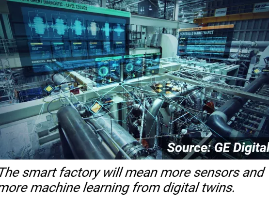
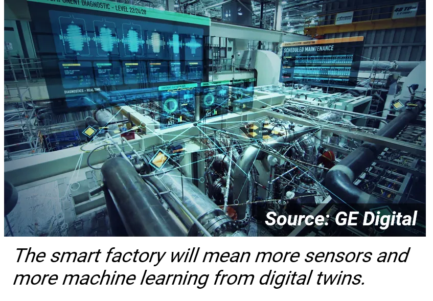
The fast-maturing hardware and software that are enabling practical applications of equipment intelligence and machine learning mean disruptive change for microelectronics manufacturing. But first comes the basic work of building the basic infrastructure, figuring out IP separation, and learning to solve physical problems in the digital world. Just how much can the semiconductor industry leverage industrial IoT practices from other industries? Common wisdom may be that industrial software solutions aren’t well suited to the IC sector’s complex needs. But GE Digital enterprise account executive Luke Smaul, currently working with Intel, argues that semiconductor fabs and toolmakers are dealing with similar issues as GE did when it first started working with Delta Airlines to monitor the GE engines on Delta planes. Smaul will speak at SEMICON West about GE’s work with Intel over the past few years and, in particular, how its solution for cloud security and IP separation can work for ICs. “GE learned to provide IP security and separation in the aviation space with its suppliers, which moved us all up the value chain, providing a big engine for growth,” says Smaul, who started his career as an IC engineer. “GE Aviation saw a 25 percent increase in issue detection rates by leveraging the same common platform. We’ve shown that we can protect Intel intellectual property in its own cloud space and control who can access what.” A toolmaker can access only particular fab data as needed for analysis, and then can reveal only the output from the analysis and a subset of supporting data. “IP separation has to happen, and it will unlock huge added value,” Smaul says. GE’s Predix solution aims to supply an easy-to-use, plug-and-play system for analytics to enable a yield engineer without a deep data background to select a supported sensor, a gateway to connect automatically to the cloud, and an analytics application to test a hypothesis of how the collected data relates to yield. “This empowers the yield engineer to use and unlock information for a quick improvement, even for simple things such as looking at the impact of degradation of fan performance over time on yield,” says Smaul. “Though the scope may be small, the impact on yield in aggregate, and when scaled, is large.” “There needs to be much more collaboration across the industry to make this work, and to share best practices,” says Smaul. “Just as GE moved from selling gas turbines to selling power-as-a-service, vendors of other big, expensive assets like IC equipment will likely change their business model from selling tools towards selling yield-as-a-service. This will simplify life for the fab while bringing the toolmaker more opportunity to sell improved capabilities on existing tools.” More human intelligence makes AI smarter Applying AI neural network approaches such as deep learning to predict outcomes from digital models is enabling disruptive advances in speech and image recognition, but applying it to complex IC manufacturing problems such as predictive maintenance has been a challenge. These neural networks require massive amounts of data to train, and the IC sector doesn’t really have big data, just a lot of little data clusters due to the dynamics and context richness of processes. This data is difficult to combine for analysis. In addition, the neural network provides only an answer but can’t explain why, notes Michael Armacost, managing director of advanced service engineering at Applied Materials. “We’ve learned that it works better if we do not ignore what we know already, but rather incorporate expert knowledge in a structured way to help us focus on the key features and the key data,” says Armacost, who will also speak in the program. This includes choosing the most important steps to include in the model, identifying the limited data to collect and how to filter the data for outliers, and then selecting the final parameters and features, adjusting the limits, and making adjustments as results drift change over time. The less data needed, the better for the complicated issue of IP protection as well. The big gains from these new analysis approaches will likely require data from more than one company and supporting security for remote connectivity. “Some end users are attempting to do the AI all themselves, but in the long term there will need to be collaboration across companies,” says James Moyne, University of Michigan professor and consultant to Applied Materials, another speaker. Collaboration will need to balance the value of the solution against the risk of compromising IP. “The low-hanging fruit are applications such as predictive maintenance in areas that do not involve high-priority IP. Another approach will be to limit the amount of shared data needed – to first build the model on a wide range of data, but then to use only a very small amount of data to operate the models.” Ready-made models could speed the process Coventor’s semiconductor process models are finding initial applications in R D whereby companies use the simulation to understand the effect of process variation on their complex designs. Instead of running dozens of actual wafers to optimize semiconductor processes, users can instead quickly simulate the results of complex process interactions on their design. Going forward, the process models could find a wide range of applications, from accelerating stabilization of new processes in the fab to enabling real-time co-optimized control across previously independent unit steps to improve wafer uniformity. “This improved uniformity across wafers and equipment could potentially reduce the need for costly physical silicon validation,” suggests Joseph Ervin, Coventor director, semiconductor process and integration, another SEMICON speaker. “Making use of in-situ metrology for real-time control also demands a digital model to process and analyze the collected data for quick response. This area has tremendous potential for improving semiconductor process control.” SEMICON West features a Smart Manufacturing Pavilion with displays and three full days of speakers on building the infrastructure needed to enable disruptive artificial intelligence in the microelectronics sector. www.semiconwest.org The SEMICON West Smart Manufacturing Pavilion features interactive Touch Liquid Crystal Displays (TLCD) and working production equipment on the floor from Bosch Rexroth, Cimetrix, Rudolph Technologies, Inficon/Final Phase Systems, OMRON, DISCO and Edwards Vacuum. For information on the SEMI Smart Manufacturing Initiative and how to get involved, please click here. Paula Doe, SEMI
Read More
Hope springs eternal. And it was with collective open arms that many U.S. businesses welcomed the recent talks between U.S. and Chinese officials to resolve their trade differences and downplay the specter of a full-blown trade war. Treasury Secretary Steven Mnuchin went so far to say that trade war with China was “on hold.”Hope and optimism soon fizzled. On May 29th, the White House released a statement contradicting Sec. Mnuchin, announcing that the Trump Administration would indeed move forward with a 25 percent tariff on $50 billion worth of goods imported from China. Besides focusing on goods that the U.S. has deemed are tied to “Made in China 2025” – the Chinese initiative to produce more advanced manufacturing goods domestically – the Administration also announced stiffer investment restrictions and enhanced export controls related to the acquisition of industrially significant technology. The final tariff list will be published by June 15th, and the proposed list of investment restrictions and export controls will be announced by June 30th.Tariffs and New Focus on Export ControlsAll of this comes as the White House and Capitol Hill have heated up their activity in recent months to curb commerce with China through tariffs and investment restrictions.The Section 301 investigation, a key component of this push, has zeroed in on China’s trade practices related to intellectual property violations. Following a months-long inquiry, the Office of the U.S. Trade Representative (USTR) determined in March 2018 that China’s forced transfer of technology and intellectual property has discriminated against U.S. firms. The finding prompted President Trump to respond with a number of remedial actions including a proposed 25 percent tariff on $50 billion worth of U.S. imports from China.More than 100 lines of the proposed tariff list directly impact the semiconductor supply chain, hitting fundamental components of the semiconductor manufacturing process. SEMI has fought back, strongly urging the removal of these tariff lines from the proposed tariff list. At a bare minimum, the tariffs against China will cost the U.S. tens of millions annually in additional taxes, create lost revenue as a result of reduced exports, threaten thousands of high-paying U.S. jobs, stifle innovation and curb U.S. technological leadership – all while not directly addressing U.S. concerns with China.These tariffs, plus the new focus on export controls, is particularly troubling for the semiconductor supply chain. The recent move comes on the heels of other trade actions, including tariffs on steel, aluminum, and solar cells that will not only limit trade and opportunities for U.S. economic growth, but also will introduce significant uncertainty for U.S. businesses. CFIUS Reform Moves Ahead, But Concerns RemainAt the same time, other government efforts that could encumber investment continue. Both the Senate Banking and House Financial Services Committees unanimously passed the Foreign Investment Risk Review Modernization Act (FIRRMA). The legislation aims to upgrade the Committee on Foreign Investment in the United States (CFIUS) – the interagency body that reviews inbound foreign investment for national security concerns. With such rare bipartisan agreement on a major bill, it is expected to be passed by both chambers and signed into law later this year.The current version of the bill is certainly an improvement on earlier drafts. The legislation no longer contains problematic language that would have given CFIUS the authority to review joint ventures between U.S. and foreign companies. The language would have, for the first time ever, expanded CFIUS’s jurisdiction to include outbound foreign investment. Given the semiconductor industry’s deep reliance on expansive global supply chains, this language was particularly concerning to our industry.However, broad concerns remain about how CFIUS functions. In recent months, CFIUS has been used seemingly to evaluate transactions based on economic security, rather than the Congressional intent of national security. Should this trend continued, we worry that this could curb otherwise acceptable investments, stifling innovation and limiting growth, especially in the semiconductor industry.SEMI Educates Lawmakers on Industry ImpactsWith tensions likely continue to rise and efforts to wall off commerce with China ongoing, SEMI is engaging with policymakers to educate them on how these restrictions will potentially undermine the long-term health of the semiconductor industry. SEMI will continue to meet with policymakers about the critical importance of trade and investment to the continued success of the semiconductor industry. If you are interested in more information on trade, or how to be involved in SEMI’s public policy program, please contact Jay Chittooran, Public Policy Manager, at [email protected].
Read More
With Southeast Asia’s semiconductor industry expected to grow up to 12 percent this year, the stakes at SEMICON Southeast Asia were high. The challenge: to drive industry connection, collaboration and innovation across a broad range of technologies to accelerate growth in the electronics manufacturing supply chain.SEMICON Southeast Asia 2018 delivered.The region's premier gathering of the global electronics manufacturing supply chain, SEMICON Southeast Asia drew an event record of more than 7,500 visitors and over 300 exhibitors to its debut at the Malaysia International Trade and Exhibition Centre (MITEC) in Kuala Lumpur. The Market Trends Briefing, an event favourite, offered insights into the latest trends and developments on forward-thinking topics as diverse as the machine as an integral part of human society (NXP Semiconductors Singapore) and intelligent robots (Festo Robotics). Key industry topics including semiconductor fab investments (SEMI) and drivers and applications for Fan-Out Wafer-Level Packaging (TechSearch International) also highlighted the briefing. 2018 Year to Date Statistics from the Market Trends Briefing For the first time, SEMICON Southeast Asia convened policy makers and industry leaders in a panel – the CXO Speaks session – that provided insights into how the region can strengthen its manufacturing ecosystem, capture new opportunities in IoT, and build a resilient and growing electronics industry. The panelists agreed that the Southeast Asia semiconductor market will continue to grow exponentially in the digital era, and that regional players must not only collaborate to sustain this growth momentum but build a strong talent pipeline to continue to drive IoT innovation.With connection clearly critical to the industry’s growth, the event’s Business-Matching sessions and industry VIP networking brought business leaders together to find new partners and opportunities.Themed ‘Think Smart, Make Smart,’ SEMICON Southeast Asia featured few devices smarter and more innovative than Festo’s AirJelly, a radio-controlled airborne jellyfish. The first indoor flying object with peristaltic drive mimics the movement of a real jellyfish – except in the air. The device’s eight tentacles adapt to its environment, just like its 500-million-year-old sea-roaming cousin. A lithium-ion battery, an electric motor and a bit of helium are its wings, allowing it to take flight.The ‘World of IoT,’ a show-within-a-show, highlighted enabling applications and technologies for the IoT revolution. This interactive experience was helmed by seven Malaysian technology start-ups that showcased present and near-future consumer technologies such as autonomous vehicles, smart AI devices and virtual reality applications enabled by semiconductor innovations.In an effort to attract STEM talent to the industry, SEMICON Southeast Asia for the first time staged a panel with 11 experts from the public sector and seven from the private sector to discuss strategies for encouraging young graduates to pursue engineering careers and building a talent pipeline. For their part, the SEMICON Southeast Asia university programme and the Electronics Talent Career Fair focused on helping to build the global semiconductor industry as it faces a worker shortage.At SEMICON Southeast Asia’s Technology Innovation Forum, thought leaders from across the industry answered the question: What does Smart Manufacturing mean to the electronics manufacturing supply chain? While presenters from GLOBALFOUNDRIES, Amkor, PricewaterhouseCoopers, Infineon, Lam, IBM, Omron, and OSRAM looked at Smart Manufacturing from very different positions in the supply chain, they shared common issues with data sharing and data protection, and decision-making methodologies when monitoring a huge influx of sensor data. Samivel Krishnamoorthy, Director of Digital Manufacturing Industrialization at OSRAM, closed the session with a real-world look at the work necessary to transition a cluster of production lines with different systems to Smart Manufacturing capable lines following common systems and data handling techniques. OSRAM embraces SEMI Standards for use in conventional silicon front-end manufacturing in for Osram’s LED production. Krishnamoorthy detailed an exceptional analysis process to benchmark and adapt best practices to complex, multi-stakeholder technology production environments.Those looking for a highly influential audience from every segment of the global microelectronics manufacturing supply chain found it as SEMICON Southeast Asia. Technology and business leaders from segments including semiconductors, LEDs, MEMS, printed/flexible electronics, and other adjacent industries were a powerful presence at the event.Held for the first time in Kuala Lumpur, the event remained true to its mission to connect electronics industry innovators and thought leaders from business, academia and research from both region and all over the world. SEMICON Southeast Asia 2019 will once again be held at MITEC.Kai Fai Ng is President, SEMI Southeast Asia.
Read More
“GlobalFoundries, TowerJazz, TSMC and UMC are expanding or bringing up RF SOI processes in 300mm fabs in an apparent race to garner the first wave of RF business for 5G, the next-generation wireless standard,” writes Mark Lapedus of Semiconductor Engineering. His recent piece, RF-SOI Wars Begin, explains why demand across the supply chain is currently tight. Rest assured, the supply situation is being addressed fast. By next year, 300mm-based RF-SOI manufacturing (vs. 200mm) will increase from 5% to 20%. But with insatiable end-user demand for greater throughput, overall RF-SOI device demand is increasing in the double-digit range, so 200mm-based manufacturing is also expanding fast. [caption id="attachment_11905" align="alignleft" width="300"] The front-end modules in all smartphones are built on Soitec's RF-SOI wafer technology. The most advanced, for LTE/LTE-A, are built on Soitec's RFeSI-SOI wafers, which have four layers to meet the demands of devices with high linearity requirements. (Courtesy: Soitec)[/caption] SOI wafer manufacturer Soitec has 70% of the RF-SOI wafer market share. The other RF-SOI wafer manufacturers – Shin-Etsu, GlobalWafers and Simgui – all use Soitec's RF-SOI wafer manufacturing technology. This is an excellent, comprehensive piece, that clearly explains the complexities of the markets, the devices, the manufacturing and the supply chain. It's a highly recommended read. BTW, the SOI Consortium is organizing a 4G/5G SOI supply chain workshop during Semicon West (July '18). Sign up or get more information on that under the Events tab here on the consortium website. Of course, here at ASN, we've been covering RF-SOI for over a decade. You can use our RF-SOI tag to access most of the pieces we've done over the years.
Read More