downloadGroupGroupnoun_press release_995423_000000 copyGroupnoun_Feed_96767_000000Group 19noun_pictures_1817522_000000Member company iconResource item iconStore item iconGroup 19Group 19noun_Photo_2085192_000000 Copynoun_presentation_2096081_000000Group 19Group Copy 7noun_webinar_692730_000000Path
Skip to main content
Part 1 of this two-part piece explores best-practice perspectives on collecting and utilizing smart data in industries outside semiconductor manufacturing, one of the important takeaways from the Smart Manufacturing panel discussion at SEMI ASMC 2018. Part 2 examines the potential benefits to be realized by pairing human Subject Matter Experts with smart silicon assistants, and what these new arrangements mean for semiconductor device manufacturing. The spacecraft Discovery and its HAL 9000 computer system had a digital twin. Did you know? Stanley Kubrick’s seminal film “2001: A Space Odyssey” had its theatrical release 50 years ago this April. “2001” isn’t just a great science fiction film. Rather, it’s a great work of cinema overall, across any category. (The American Film Institute lists “2001” as #15 in the AFI Top 100; a bit below “Vertigo,” a bit above “It’s A Wonderful Life.”) It’s a film so distinguished and so prescient that its lessons can inform our thinking about smart manufacturing, Industry 4.0, and artificial intelligence (AI) today. Not to give too much away, but the earth-bound digital twin of Discovery / HAL identifies a diagnostic error the onboard, Jupiter-bound HAL 9000 has made, things go awry from there, and one of the mission pilots, astronaut Dave Bowman, is forced to intervene. At the recent SEMI Advanced Semiconductor Manufacturing Conference, ASMC 2018, on 02 May 2018 in Saratoga Springs, NY, five diverse panelists representing capital equipment, IDMs, academia, the semiconductor supply chain, and smart manufacturing best practices outside the semiconductor industry engaged in a lively discussion with the ASMC attendees. They explored where “smart” is in our industry today, where it’s headed, and what that’s going to mean for us -- the professionals who have brought semiconductor manufacturing to the current state of smart, and are looking to implement an ever-smarter tomorrow. Not to give too much away, but the panelists and audience agreed that there’s nothing artificial about pairing human intelligence with machine-based smart manufacturing. Implementing an ever-smarter tomorrow in semiconductor manufacturing requires smart people just as much as it requires smart machines. 
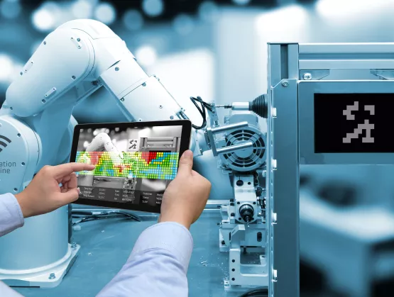
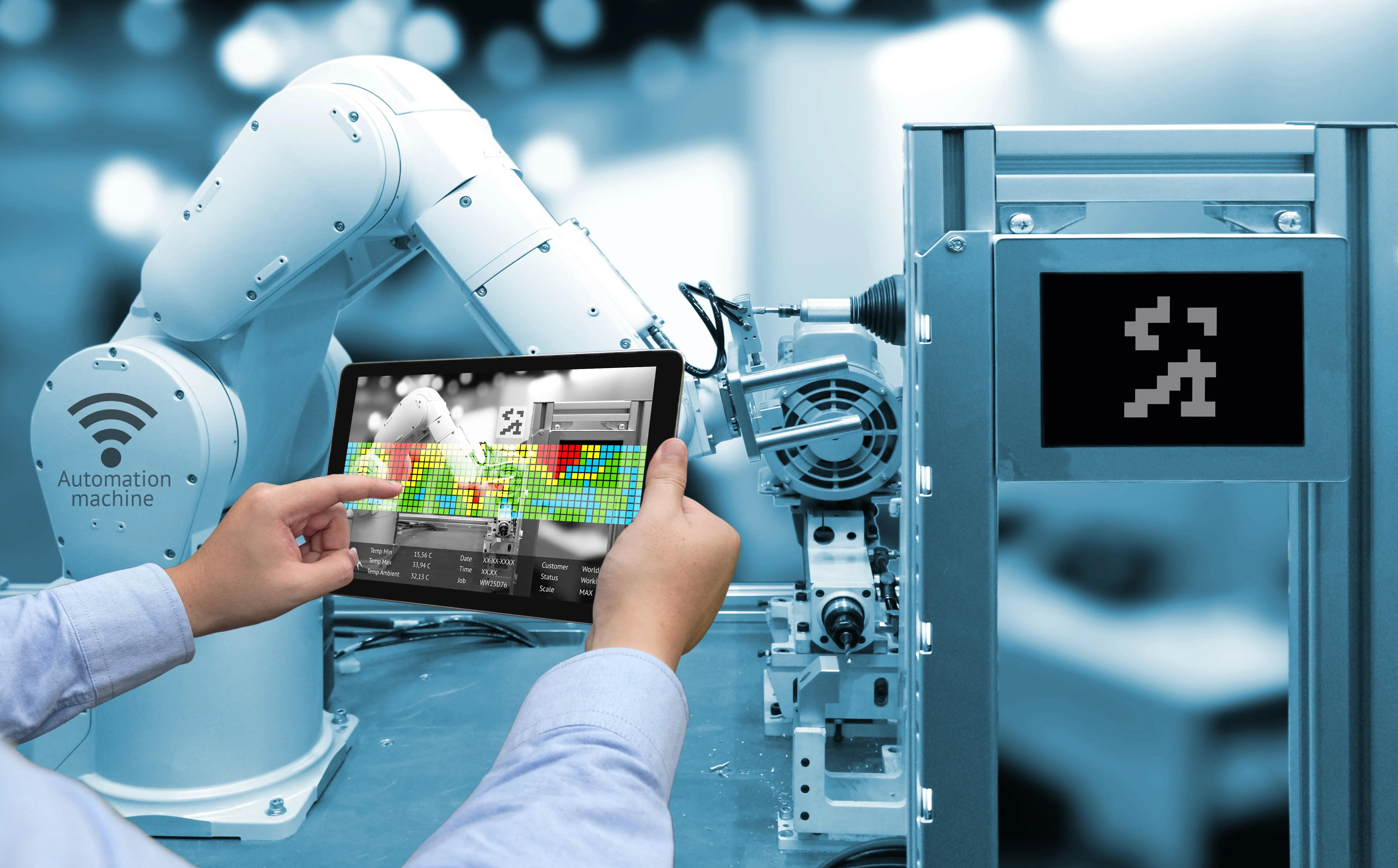
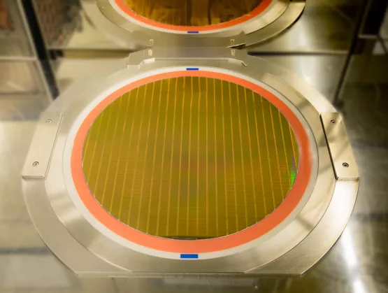
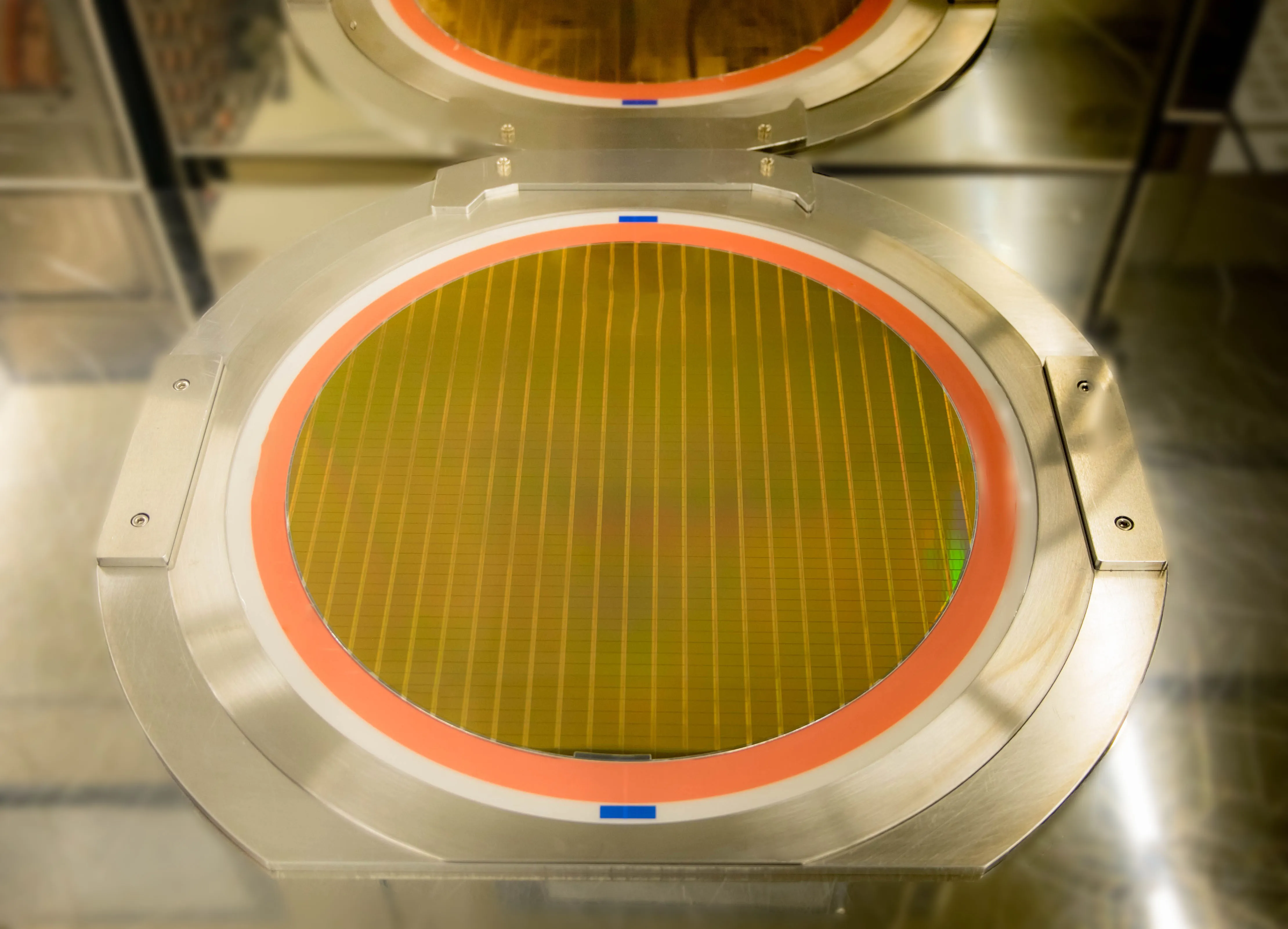
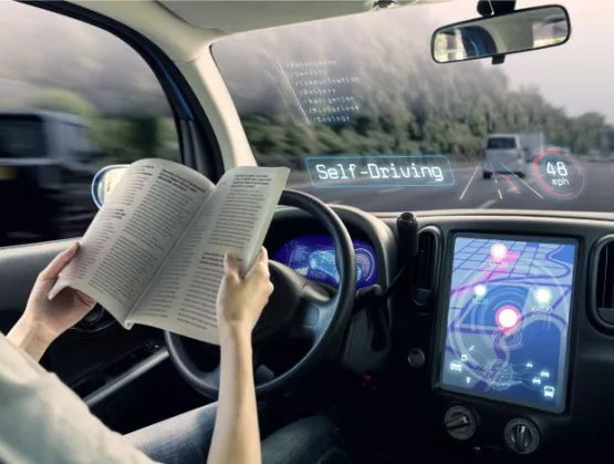
Moving towards “smart” means understanding how to derive useful information and actionable intelligence from the ever-increasing pool of big data created during semiconductor manufacturing. Modern manufacturing sites are extensively instrumented today, and create massive amounts of data to consume, decipher, base decisions upon, or discard. As we dig into this problem we realize that equipment and processes in our industry are both obviously complex, but, also, subtly complex. Semiconductor manufacturing tools easily contain 100s to 1000s of components working together to produce nanometer scale, angstrom scale, or even atomic scale features using complex chemical, physical, and plasma processes. There is a plethora of potential failure points and modes, and despite our best efforts to collect more data, many processes continue to be only poorly observable. On top of that, semiconductor fabrication processes are always drifting, and the operational context is continually changing as we change product mix, process maintenance swap-out kit components, and operating conditions and recipes. Sounds like … hospitals, and healthcare? When you see your doctor, she will collect and look at your instrumented data – blood work, blood pressure, weight, and other quantifiable factors. But, typically, your doctor won’t draw a conclusion based on that analysis alone. Rather, your doctor will sit with you, ask probing questions, and record what she asked, your responses, and what she saw, what she heard, and what she thought. Then she’ll build a hypothesis, combining the “anecdotal” data with the instrumented data, and derive from that data set both a likely diagnosis and an effective course of action. In this case, beyond the instrumented data, two humans, and their natural language input, are part of the equation: the patient, with his observations and thoughts, as well as the doctor, with hers. And it’s been a formula for success. Healthcare has made huge, step-function improvements across a spectrum of deadly diseases, as well as with less-deadly chronic afflictions, by harvesting this complex input, committing the proven disease presentation – disease diagnosis – and disease treatment models to medicine’s collective memory, and then teaching the next generation of healthcare providers both the general methods and the standard protocols essential to maintaining good health and successful outcomes. Maybe, in medicine, what seems a big data environment is really just clusters and clusters of loose small data connected by the collective neural network of highly trained doctors and their colleagues. Nancy Greco (IBM Watson), Dave Mayewski (Rockwell Automation), James Moyne (University of Michigan / Applied Materials), and Paul Werbaneth (Intevac, Inc.), along with Julie Jacob (Ernst Young), and Carson Henry (Micron Technology), were members of the SEMI ASMC 2018 panel discussing Industry 4.0 and the Future of Commercial Semiconductor Device Manufacturing. All opinions here are purely our own. Please contact Paul Werbaneth via email at [email protected]. The SEMICON West (July 9-11, 2018, in San Francisco) Smart Manufacturing Pavilion features working production equipment on the floor and three full days of speakers providing insights on building the infrastructure needed to enable AI. Equipment from Bosch Rexroth, Cimetrix, Rudolph Technologies, INFICON, Final Phase Systems, OMRON, DISCO and Edwards Vacuum will showcase cutting-edge smart manufacturing technologies. For information on the SEMI Smart Manufacturing initiative and how to get involved, please click here.
Read More
Chip testing is becoming smarter and more complex, creating growing requirements to stream data in real time and ensure it is ready to use for analysis, regardless of the vendor source. Adaptive testing using machine learning to predict die performance in a downstream test can reduce the number of cycles by as much as 40 per cent without compromising test performance, notes Dan Sebban, VP of data analysis, OptimalPlus, who’ll speak on machine learning challenges at SEMICON West’s Test Vision 2020 program. “As devices and their test requirements grow in complexity, the motivation for automating adaptive test greatly increases,” he states, adding that characteristics such as die location on the wafer, defects on neighboring die, condition of the tester, and test values near the specification limits can help predict which die are likely to be good.“The big issue we see is that while everyone likes the idea of machine learning, it remains a black box model, with little visibility into why it makes the decisions it does,” adds Sebban. In addition, a suitable infrastructure to run, deploy and assess a machine learning model in real time is required. “There is still some hesitation to adopt machine learning. It’s a big change of mindset. While building the confidence to use machine learning will take time and experience, using the technology to automate big data analysis with the relevant infrastructure may be our best alternative to reduce test cost.” Systems test and parts-per-billion quality become the ruleSystems test will continue to become more prominent and more complex as chips and packages shrink, affirms Stacy Ajouri, Texas Instruments system integration engineer and Test Vision 2020 event chair. “Even IC makers now need to start doing more systems test.” And as more ICs are used in automotive applications, the distinction between consumer and automotive requirements is blurring, driving demand in other markets for higher precision test with parts-per-billion defectivity requirements.“Intelligent test gets increasingly challenging as devices become more complex and as testing moves from distinguishing good from bad devices to figuring out how to repair and trim marginal devices to make them good,” adds Derek Floyd, Advantest director of business development, this year’s program chair. “We’re highlighting efforts to create the infrastructure the industry needs to manage big data for machine learning with test platforms from different vendors,” says Ajouri, citing work on new standards for streaming data from the testers and labeling critical steps in consistent language to simplify the use of data from different platforms in real time. “I have 10 platforms from multiple vendors, and I need them to mean exactly the same thing by ‘lot’ so I don’t have to sort it out before I can use the data,” she says.Are devices becoming too complicated to test at the required price point?Can testing be economical with up to a million die per wafer, 50 data points per die, a requirement for parts-per-billion accuracy, and the need to identify parts that test good now but that might fail in the future? Organizers of the event invite chipmakers and test suppliers to debate the issue. “The speed of innovation in the semiconductor industry challenges test to keep pace,” notes Floyd. “The product we’re testing is always ahead of the product we have to test it with.”The two-day event features sessions on automotive test; big data and machine learning for adaptive test; handling and interface issues such as over-the-air testing; and a general session covering memory and RF test.Paula Doe, SEMI
Read More
The MCU at the heart of Sony's new smart-sensing SPRESENSE™ for IoT is built on FD-SOI. Why? Low operating voltage and low power consumption, of course! Sony's got two cool new products going on sale in July 2018: the SPRESENCE main and extension boards for IoT applications, equipped with a smart-sensing processor (read the full press release here). A CXD5602PWBCAM1 camera board for sensing cameras will go on sale in August. All were on display at the SF Maker Fair '18, where they were an instant hit. [caption id="attachment_11931" align="alignright" width="300"] Here are the main features of Sony's CXD5602 MCU for IoT, which is built on FD-SOI. (Courtesy: Sony Semiconductor Solutions)[/caption] The main board (it's open source, btw) will run about US$50. You'll find the specs and main features here. Spresense is powered by Sony's FDSOI-based CXD5602 MCU (ARM Cortex-M4F × 6 cores), with a clock speed up to 156 MHz. The main board utilizes a multi-CPU structure equipped with Sony's state-of-the-art GNSS (Global Navigation Satellite System – which they talked about at the most recent SOI Symposiums in SF and Tokyo) receiver. A variety of systems for diverse applications, including drones, smart speakers, sensing cameras and other IoT devices, can be built by combining these boards and developing the relevant applications. The new board can be used to control a drone, for example, using GPS positioning technology and a high-performance processor, voice-controlled smart speakers, low-power consumption sensing cameras and other IoT devices, etc. It can also be combined with various sensors for use in systems that detect errors in production lines on the factory floor.
Read More
The fast-growing automotive semiconductor market means big change for the IC supply chain. Beyond the obvious demands for reliability and traceability, the sector is moving towards simpler and lower-cost solutions while facing the daunting challenge of automating driving in a complex world. The need for simpler and cheaper automotive intelligence will likely drive acquisitions to build complete platform solutions that are easier to integrate. This demand has already spawned a market for pre-configured test cars to save developers time and money, and is driving LiDAR (Light Detection And RADAR) towards lower-cost, solid state solutions. “The growth of the automotive electronics market provides a great opportunity for the IC supply chain to differentiate on specialty processes and quality for the high-volume automotive business with its long design cycles,” says Scott Jones, principal, strategy, at KPMG, who will speak in the automotive program at SEMICON West. “This differentiation is a chance to reduce chip suppliers’ dependence on scaling volume for the mobile phone world with its short-cycle volatility of winning and losing sockets.” He notes that increasing demand for automotive ICs is also reinvigorating the eight-inch supply chain and spurring opportunity for specialty products such as compound semiconductor devices for power efficiency. Supplying the automotive market also means addressing automotive reliability requirements, which can be 10 times more stringent than for consumer devices. At the same time, the industry must sustain fast-paced development cycles required for the volume and diversity of low-cost IoT devices, manage the segmented supply chain for both those markets, and still spread development costs. Another big challenge for the supply chain will be to automate testing and update vast amounts of embedded software in these automotive devices. “The more complete solution a company can put together, the more the automakers will gravitate to it. They want simplicity,” Jones suggests. Smaller players will need to differentiate with IP and acquire other IP provider to build a broader platform, or be acquired and folded into an all-in-one solution.AutonomouStuff helps accelerate and simplify development of autonomous driving solutionsAutonomouStuff is helping to speed development of these platforms. The company has grown from a sensor distributor into a supplier in the emerging niche of vehicles preconfigured with key interfaces for sensors and controls. These interfaces can then be customized by integrating different components for developers to test their applications. AutonomouStuff offers developers a lineup of vehicle models pre-configured with the interfaces needed to add desired chips, sensors and software to develop their autonomous vehicle systems. Source: AutonomouStuff.“Whether they’re major chipmakers or AI software startups, they don’t have a year to build their own vehicle platforms themselves for developing autonomous vehicle systems,” says Wolfgang Juchmann, VP sales and business development at AutonomouStuff. Juchmann, a SEMICON West speaker, will bring a demonstration vehicle to the show. “In four to six weeks we can prepare a custom test car with selected sensors, enabling users to start testing their computer platforms and software. It’s faster and more cost-effective for us to supply the car with the needed interfaces.” He notes that developers are using some 300 AutonomouStuff vehicles in the field. AutonomouStuff customers are starting to transition from testing on a single car or two to testing on mini-fleets with 50 to 100 vehicles. Beyond sensors and pre-configured vehicles, the next step will be to add more data intelligence services to help with capabilities like tagging the data for training, Juchmann says. AutonomouStuff already offers hardware to support Baidu’s Apollo open-source software stack and data set. The company was recently acquired by the Swedish holding company Hexagon to help support expansion.CMOS silicon LiDAR nears automotive qualificationInnovations in the hyper-competitive LiDAR market, where burgeoning demand is driving the race to develop various types of solid-state devices, may also help reduce the cost of autonomous vehicles. Among the roughly 40 LiDAR suppliers, at least one – Quanergy – is taking advantage of 45nm and 32nm foundry CMOS volume production. The company uses voltage through the semiconductor stack to change the refractive index, controlling the phases of optical beams and the resulting interference patterns of light exiting the chip to quickly steer the laser beam without the need for moving parts, much like the phased array radar its team developed earlier. Solid state LiDAR image with object recognition software. Source: QuanergySo far, most of the small LiDAR units have shipped to the security, industrial automation, drone, robots and 3D mapping markets. However, Quanergy CEO Louay Eldada, another SEMICON speaker, says the company is also winning automotive designs and expects automotive shipments to take off early next year, once automotive certification testing is completed. “We can get design wins because standard CMOS production at TSMC makes us a known entity,” says Eldada. To prevent component misalignment, the company produces its own specialized packaging to secure the laser, phase control ASIC, optical phased-array emitter, detector array, and receiver readout ASIC at its plant in Silicon Valley or the facility of its automotive partner Sensata. Through its software business, Quanergy offers an artificial intelligence (AI) perception program for object recognition and LiDAR tracking. The solution uses the people-tracker software the company acquired from Raytheon.SEMICON West this year expands to three full days of automotive electronics programming and features a Smart Transportation Pavilion. Other companies with experts who will speak as part of the program include XPT/NIO, Infineon, McKinsey, Voyage, GM Cruise, Bosch, Deepen AI, Airbus A3, Nvidia, Excelfore, Byton, Macronix, SK Hynix, SAP, Xilinx, Achronics, California Fuel Cell Partnership, Velodyne, Lam Research, KLA-Tencor, SCREEN, Rockwell, Versum Materials, TechSearch International, Entegris, ASE, Amazon, Continental and Wind River. www.semiconwest.orgPaul Doe, SEMI
Read More
Device manufacturers continue to invest. Spending in cloud data center (compute, networking and storage), automotive (content per car increases), industrial (on content, factory automation, and positive macro trends), and consumer (gaming) end-markets is particularly strong. We see capital expenditure growth in 2018 and early indications pointing to sustainable spending into 2019. We also expect 14 percent increase (YoY) for fab equipment spending in 2018, up from the February forecast of 9 percent, and expect 9 percent increase in 2019, adjusted from the February forecast of 5 percent. 92 future facilities/lines with various probabilities are scheduled to start production in 2018 or later. Fab investment is just one indicator of how growing demand in areas such as from Artificial Intelligence (AI), cloud/data storage, automotive and Internet of Things (IoT) is driving unprecedented spending in the semiconductor industry. Below are a few highlights* of recent SEMI FabView insights. Details of each project can be found in FabView online 24/7 or World Fab Forecast report (Excel format). Infineon’s new 300mm Fab in Austria - Infineon is planning a new 300mm thin wafer Fab for Power Devices in Villach, Austria. Rumors on Toshiba’s new Fab plans - More 3D NAND fabs in the future at Toshiba are feasible. The timing will depend on market conditions, and our forecast will adjust accordingly. Vanguard's possible 300mm foundry fab - Vanguard's management said it might buy or build a 300mm fab in the near future as all 200mm fabs are essentially full. Powerchip plans to build new memory fab in Taiwan - Powerchip is investing more in expansions since Memory pricing is holding up. Rohm announced to build a new SiC fab in Fukuoka Japan - Rohm announced its plans to build a new SiC fab. Micron is building a new fab in Singapore - Micron broke ground in a ceremony for a new fab in Singapore on April 4, 2018. Bosch had groundbreaking ceremony of their 300mm fab in Dresden end April 2018 - Investment of 1 billion Euro. This is the biggest single investment in Bosch’s 130-year history. SEMI FabView, a mobile-friendly, interactive version of SEMI’s popular World Fab Forecast, delivers on-demand fab information such as fab spending and capacity for over 1,100 facilities, including over 82 planned facilities worldwide, across a wide range of product segments including Power, GPU, Memory, Foundry, MEMS and Sensors fabs. Fab data include region, start of construction, operation, construction and equipment spending, capacity, wafer sizes, product types and geometries. SEMI FabView subscribers receive forecast model updates through SEMI’s World Fab Database. Click here for a trial to experience SEMI FabView first hand. *Actual updates provide more detail Christian G. Dieseldorff and Clark Tseng, Industry Research Statistics Group, SEMI.
Read More
The U.S. Trade Representative (USTR), based on findings from its Section 301 investigation into China's trade practices, today announced a 25 percent tariff on $34 billion in Chinese goods including many products in the semiconductor supply chain.Products such as test and inspection equipment and spare parts that enter the U.S. from China will be subject to this tariff, which enters into force on July 6, 2018. About 80 percent of the semiconductor products originally proposed remain on the final list of tariffs.USTR also has proposed tariffs on more than $16 billion worth of goods including chemicals as well as machines and spare parts that are used to manufacture semiconductor devices, wafers, flat panel displays, and masks, all of which would squarely strike the semiconductor industry. This new proposed list includes products identified by the U.S. government that have particularly benefited from Chinese industrial policies such as “Made in China 2025.” SEMI is set to voice its opposition to these tariffs with written comments and at an upcoming public hearing.Over the past month, SEMI has submitted written comments and offered testimony on the damaging impact that tariffs would have on the U.S. semiconductor industry. While SEMI strongly supports efforts to better protect valuable intellectual property, we believe that these tariffs will do nothing to address U.S. concerns over China’s trade practices. Instead, the tariffs will harm companies in the semiconductor supply chain by increasing business costs, introducing uncertainty and stifling innovation.SEMI will continue to engage with lawmakers as the $34 billion in tariffs take effect and the proposed $16 billion in duties remain under consideration. We encourage members to review this list and determine the level, if any, of impact. If you have questions or concerns, please reach out to Jay Chittooran, Public Policy Manager at SEMI, at [email protected].
Read More
Updated Global GDP ForecastThe World Bank just updated its multiyear forecast for GDP growth both globally and by country (Chart 1).It noted: “Despite recent softening, global economic growth will remain robust at 3.1 percent in 2018 before slowing gradually over the next two years, as advanced-economy growth decelerates and the recovery in major commodity-exporting emerging market and developing economies levels off.“This outlook is subject to considerable downside risks. The possibility of disorderly financial market volatility has increased, and the vulnerability of some emerging market and developing economies to such disruption has risen. Trade protectionist sentiment has also mounted, while policy uncertainty and geopolitical risks remain elevated.”www.worldbank.orgSemiconductor Growth Outlook Strong (Chart 2)The WSTS updated its world semiconductor shipment forecast. This new forecast (endorsed by SIA) projects worldwide semiconductor sales will be a record $463 billion in 2018, a 12.4 percent increase from 2017. WSTS projects year-to-year increases across all regional markets for 2018.This revised semiconductor forecast coupled with very robust global semiconductor capital equipment sales (Chart 3) paint a positive outlook for 2018.www.semiconductors.orgwww.semi.orgVery Strong End Market Growth in First Quarter (Chart 4)Based upon the combined 1Q’18 financial reports of 213 large, global OEMs, electronic equipment sales (consolidated into U.S. dollars) increased globally an estimated (and very robust) 10.6 percent in 1Q’18 vs. 1Q’17. While this world growth result is very heartening it was significantly inflated by exchange rate effects as stronger non-dollar currencies were converted into weaker dollars. Looking at world electronic equipment sales consolidated into both dollars and euros, 1Q’18 growth rates are MUCH different (Chart 5). 1Q’18 vs.1Q’17 electronic equipment sales grew 10.6 percent in dollars but declined 4.3 percent in euros! Certainly the first quarter was strong globally but the currency chosen for analysis can have a BIG effect.U.S. Supply Chain Expansion ContinuesLooking at the U.S. market (in dollars - therefore not distorted by exchange rates) domestic electronic equipment orders rose 6.7 percent in February-April 2018 versus the same three-month period in 2017. The U.S. electronic industry is doing reasonably well at present.www.census.gov/manufacturing/m3/Expect the recent exchange rate based amplification of dollar denominated global growth to taper off quickly.Keep a careful watch on the geopolitical situation.Walt Custer of Custer Consulting Group is an analyst focused on the global electronics [email protected]
Read More
[caption id="attachment_11914" align="alignright" width="150"] Mark Granger, GlobalFoundries' VP Automotive Product Line Management[/caption] GF's 22FDX® (22nm FD-SOI) offering is on an automotive roll. The technology platform has been certified for several key automotive standards, and GF has announced an exciting new ADAS customer in Arbe Robotics. In addition to sharing info from various press releases and blogs, ASN also had a chance to catch up with Mark Granger, GF's VP for automotive, who provided some great insights. Read on! Taking the Heat When it comes to compliance, automotive industry standards are excruciatingly rigorous. Every part that goes into a car must adhere to the relevant standards: chips are no exception. One such standard is the AEC – Q100, a “Failure Mechanism Based Stress Test Qualification For Integrated Circuits”. The AEC – aka the Automotive Electronics Council – handles those testing standards and certification. Grade 2 means a technology is certified for the -40°C to +105°C ambient operating temperature range. To achieve Grade 2 certification, devices have to successfully withstand reliability stress tests for an extended period of time over the specified temperature range. GF recently announced that 22FDX has been AEC Q100 Grade 2 certified (press release here). However Granger adds that for their customers, they've added additional headroom that takes them to 125°C. They're now working on Grade 1 certification, he says, which means the devices are certified to handle junction temperatures up to 125°C (and there again, GF has added additional headroom that takes them to 150°C). That should be done by the end of 2018. The ability you get with FD-SOI to tune the transistors using body biasing is really beneficial here, he says. For GF, the 22FDX qualifications exemplifies their commitment to providing high-performance, high-quality technology solutions for the automotive industry. The automotive industry is driven by a “zero excursions – zero defects” mindset, says Granger, and that drives the foundry, too. SOI has been used for decades across industries where heat and electromagnetic radiation are challenges, bringing soft error rates (SER) down by orders of magnitude, notes Granger. (SOI, btw, essentially eliminates what are known as Single Event Upsets (SEU) caused by latch-up, which in turn brings down SER.) That in turn, ties into the FIT (failure in time) rate – and that's part of the ISO 26262 “Road vehicles – Functional safety” standard – where 22FDX is also certified. As a part of GF's AutoPro™ platform, 22FDX allows customers to easily migrate their automotive microcontrollers and ASSPs to a more advanced technology, while leveraging the significant area, performance and energy efficiency benefits over competing technologies. Moreover, the optimized platform offers high performance RF and mmWave capabilities for automotive radar applications and supports implementation of logic, Flash, non-volatile memory (NVM) in MCUs and high voltage devices to meet the unique requirements of in-vehicle ICs. GF's Fab 1 in Dresden, Germany (which is where they do 22FDX) also has achieved ISO-9001/IATF-16949 certification, which demonstrates that it is capable of meeting the stringent and evolving needs of the automotive industry. (IATF is the International Automotive Task Force. 16949 is a Quality Management System (QMS) certification specifically for the automotive sector.) Granger wrote a really informative blog on the GF website – you can read it here. It includes this graphic, indicating where in the car 22FDX-based parts are expected to go. [caption id="attachment_11913" align="alignleft" width="1000"] Here's how GF sees the applications for 22FDX and other chip technologies in automotive applications. (Courtesy: GlobalFoundries)[/caption] On Radar GF recently announced that Arbe Robotics selected 22FDX® as the process technology for its groundbreaking patented imaging radar. Arbe aims to achieve fully automated system capabilities and enable safer driving experiences for autonomous vehicles (read the press release here). As the first company to demonstrate ultra-high-resolution at a wide field of view, Arbe Robotics’ radar technology can detect pedestrians and obstacles at a range of 300 meters, in any weather and lighting conditions. The processor creates a full 3D shape of the objects and their velocity, and classifies targets using their radar signature. As Granger noted in his blog, “Radar is one of several sensor types used to detect objects near a vehicle, to enable features like adaptive cruise control. Lidar is another. It uses pulsed lasers to determine distance from an object by measuring the time it takes for the light to reflect back. However, lidar is currently expensive and is affected by weather conditions. Radar is less expensive, and higher-resolution radars promise to compete well with lidar in automotive applications, thereby enabling lower-priced vehicles to enjoy greater ADAS capabilities. 22FDX-based radar sensors can provide higher resolutions and less latency than current radar sensors at a very low total system cost.” While they may be complementary at first, there is a battle brewing between high-resolution radar and lidar, Granger told ASN. Putting their solution on 22FDX enables Arbe to achieve a 77 GHz mmWave radar and compete cost-effectively with lidar. “They wanted the best,” says Granger. 22FDX can achieve the requisite Ft and Fmax figures of merit. And with transistor stacking, they can also integrate the power amplifier (PA) on a single device. With the low inherent capacitance of the PA in 22FDX, you can get the high power output you need for mmWave but with low power consumption. GF blogger Dave Lammers has also written a great piece about the Arbe solution (you should read it: here's the link). “The company said its advanced technology allows the detection of small targets, such as a human or a bike even if they are somewhat masked by a large object such as a truck,” he writes. “The imaging radar can determine whether objects are moving, and in what direction, and alert the car in real-time about a risk. “While other car sensors can fail when it is raining, if there’s fog, and due to blinding lights such as a sudden reflection, Arbe’s radar is completely oblivious to all those factors. The custom designed radar processor creates a full real-time 4D image of the environment, and classifies targets using their radar signature.” Avi Bauer, Arbe's VP of R D, is now clearly an SOI fan. Lammers quotes him as saying, “With SOI the design is more straightforward, and (voltage) biasing allows you to do things that cannot be done in standard CMOS. For the transmit and receive modules, SOI’s higher resistivity substrate benefits the passive components – inductors and capacitors – and allows good isolation. High Q passives are important. At 22nm, SOI allows better performance overall.” Clearly good things are coming down the road for FD-SOI!
Read More
The Scaling Technologies TechXPOT at this year’s SEMICON West (Scaling Every Which Way! – Thursday, July 12, 2:00pm-4:00pm) will explore traditional scaling as the industry marches toward 3nm and beyond, as well as technologies that enable 3D architectures, die stacking, and interconnect scaling. The session will also provide an update on how the various players (foundry, IDM, fabless, and application developers) are jockeying for innovation leadership. As a prelude to the event, SEMI asked Priya Mukundhan, director, Technology Development and Applications, at Rudolph Technologies, and a speaker at the TechXPOT, to provide her insights into challenges associated with metrology and inspection.For a full list of speakers and program agenda, visit http://www.semiconwest.org/programs-catalog/scaling-every-which-way. Priya Mukundhan, director, Technology Development and Applications, Rudolph TechnologiesSEMI: What are the key challenges that need to be addressed to provide the kind of metrology and inspection solutions that will be needed by the industry as scaling – in all its forms (e.g., traditional, 3D ICs, interconnect, and different transistor architectures) – is pursued at 5nm and then at 3nm? Priya Mukundhan: With respect to metrology needed to scale FinFETs, the following will be key: Gate critical dimension (CD) at the fin sidewall, gate height, gate profile Fin CD, height and profile Dopant profiles Stress measurement in the fin Composition in thin film and interface These challenges are currently being handled using in-line CD solutions, CD scanning electron microscopy (CD-SEM) and CD atomic force microscopy (CD-AFM), along with optical critical dimension (OCD) measurements. There is no single technology that can take all of these measurements, and determining the right solution is application-dependent[1].Issues associated with inspection and scaling include the following: Bright-field inspection lacks the sensitivity to detect defects smaller than those found at the 20nm node Detecting defects that are 5nm or smaller is achieved using electron beam inspection tools, but these single-electron beam inspection systems are prohibitively slow and cannot meet the high-volume manufacturing (HVM) requirements for defect inspection Buried defects Void detection in 3D SiP structures, front and backside inspection Sidewall crack detection in packaging SEMI: Can you provide a summary of the R D roadmap for metrology/inspection tools that you see emerging in order to get to 3nm? PM: Hybrid metrology is currently in use, especially for CD metrology. To support the development efforts, techniques that provide complementary information as well as those that eliminate uncertainties will be required. Researchers at imec[2] have started exploring technology combinations to gain insight into how new structures function. Some of the findings in imec’s study include the following: The combination of transmission electron microscopy (TEM) and scanning probe microscopy (SPM) provides a unique approach of imaging combined with a functional analysis capability In situ SPM could potentially determine composition (SIMS) as well as functional properties (electrical) Fast Fourier transform scanning spreading resistance microscopy (FFT-SSRM) is a novel technique that measures carrier profiles in semiconductors. This overcomes the current SSRM limitations of signal distortions due to parasitic resistances while measuring on small volumes such as FinFET and nanowires Multi-electron beam inspection can be used for HVM for sensitivity to smaller SEMI: How will metrology and inspection be impacted beyond 3nm? What kinds of tools will be needed by that point in time?PM: There are several different transistor options that have been identified by leading edge wafer fabs and consortia looking beyond the 5nm node roadmap[3,4]. Some of the options on the table include the following: 1) Extension of the current FinFET in the form of gate-all-around FET2) Creating them with new materials by adding ferroelectrics (e.g., negative capacitance FET, or NC-FET) 3) Complementary FET4) Vertical nanowires and nanosheet FETsThese possibilities bring new challenges and require characterization at the material level. Also, the industry as a whole will have to redefine what it means to do composition at the nanometer level. This could be the beginning of a trend towards array-based metrology, i.e., measurements on an array of devices to gather statistically significant data[2].Regarding metrology needs at 3nm, it is too early to determine what kind of tools would be needed only for R D and how many of them would need to be extended to high-volume manufacturing (HVM). From an inspection perspective, there will be a continued migration towards computer aided design (CAD)-based inspection, as well as having the ability to deal with large image data sets (petabyte, big data). Furthermore, inspection algorithms should be improved, along with better staging for better image stitching.References Bunday, E. Solecky, A. Vaid, A. F. Bello, X. Dai, “Metrology capabilities and needs for 7nm and 5nm logic nodes,” Proc. Of SPIE, Vol. 10145, 101450G, pp. 1-41, 2017. Imec roadmap and imec magazine. Intel roadmap. https://semiengineering.com/transistor-options-beyond-3nm/ Debra Vogler, SEMI
Read More
Self-driving cars have been all the rage in both the trade and popular press in recent years. I prefer the term “autonomous vehicles,” which more broadly captures the possibilities, encompassing not only small passenger vehicles but mass transit and industrial vehicles as well. Depending on who’s talking, we will all be riding in fully autonomous vehicles in five to 25 years.The five-year estimates come from startups eager to raise venture capital while the 25-year estimates stem from Tier 1 automotive suppliers who tend to be more conservative in outlook. Regardless of the timeframe, a multitude of investors – national governments, venture capitalists and companies – are dedicating significant capital and effort to make autonomous vehicles a reality.I must admit that I did not fully grasp the enthusiasm for self-driving cars until last year. First, I’ve always enjoyed driving, unless I’m in stop-and-go traffic, so I couldn’t imagine relinquishing the task. Second, I’ve deliberately arranged my life to spend minimal time in my car. However, traffic has become much heavier in my metropolitan area (Boston), and I know that many people in cities around the world face longer commutes and waste more time in gridlock.What is the solution to this problem that is only getting worse? I had an epiphany while walking through Shinigawa Station in Tokyo, one of the busiest train stations in the world. Dense streams of people crisscrossed the station on their individual paths, managing to avoid collisions without the aid of traffic controls. Evidently, humans have an innate collision-avoidance ability that makes traffic controls for pedestrian crowds unnecessary. If autonomous vehicles could achieve the same excellence in collision-avoidance, we could potentially reduce or eliminate traffic controls for vehicular traffic, providing a huge gain in transportation efficiency and relief from gridlock.Sensors as core building blocksNew and improved sensors, many based on micro-electromechanical systems (MEMS) technology, are key to achieving this vision. While MEMS inertial sensors (such as accelerometers and gyros) are already integral to the core safety systems in conventional vehicles, they are also essential to improved self-navigation in autonomous vehicles.The challenge for MEMS suppliers is to deliver inertial sensors that meet the requirements for self-navigation systems, which are different and more demanding than for safety systems.Pinpointing a vehicle’s position requires “dead reckoning” based on inertial sensor signals as a supplement to GPS input. Undesirable drift in the inertial sensor signals due to mechanical quadrature, temperature sensitivity and noise can quickly add up to a large error in position that may result in a collision. To meet the more rigorous requirements for autonomous vehicles, suppliers must design MEMS inertial sensors that are substantially more precise and resistant to drift. This requires design software that is both extremely accurate and fast, as well as increasingly precise and reliable manufacturing capabilities.Other MEMS-based devices, such as micromirrors and micro ultrasound transducers (MUTs), are also promising options for implementing vision and range-finding systems in autonomous vehicles. These sensing systems are needed for building electronic versions of the human collision-avoidance abilities that I witnessed in Shinigawa Station – and it is these systems that autonomous vehicles must emulate.When will self-driving cars become a reality? Aside from the provocative question that got you to read this far, I don’t have a definitive answer. It will undoubtedly occur in phases, ranging from the driver-augmentation systems available in today’s cars to the full autonomy and ubiquity that will allow reduction of traffic controls in 20 years or more. It is clear that the ultimate goals for autonomous vehicles are highly worthwhile, and that achieving those goals will require better-performing and more diverse MEMS sensors. Stephen (Steve) Breit, Ph.D. is Senior Director, MEMS Business, at Coventor, a Lam Research Company. Steve has been responsible for overseeing development and delivery of Coventor’s industry-leading software tools for MEMS design automation since joining Coventor in 2000. Steve holds numerous patents on software systems and methods for MEMS design automation and virtual fabrication. He holds a Ph.D. in Ocean Engineering from MIT and a B.S. in Naval Architecture and Marine Engineering from Webb Institute.For more information, visit: https://www.coventor.com
Read More