downloadGroupGroupnoun_press release_995423_000000 copyGroupnoun_Feed_96767_000000Group 19noun_pictures_1817522_000000Member company iconResource item iconStore item iconGroup 19Group 19noun_Photo_2085192_000000 Copynoun_presentation_2096081_000000Group 19Group Copy 7noun_webinar_692730_000000Path
Skip to main content
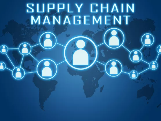
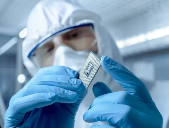
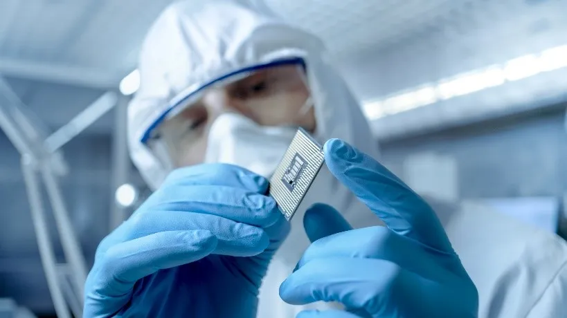
Would you buy your next hotdog in parts, from un-coordinated suppliers? For example: Get the bun from a baker, the sausage from a butcher, mustard and/or ketchup and veggies from the nearest supermarket? If yes, you may find the sausage being too small, the veggies too big for the bun, and, when you finally finished adding mustard/ketchup and start eating, you may “enjoy” a cold sausage on a soggy bun!This “hotdog example” is just a very simple way to highlight the advantages of a well-coordinated semiconductor supply chain. What may be a few dollars and cents wasted in this hotdog purchase, can become millions of dollars lost to delays and inefficiencies during the roll-out of a new electronic system.Complexity is Increasing the ChallengeThe very innovative semiconductor industry is continuing to develop more complete and complex building blocks for electronic system solutions, with the intent of making our customers’ lives easier. However, every new technology takes increasingly more time for technical and business interfaces to mature before all the semiconductor supply chain members can serve customers in a smooth, efficient and cost-effective manner. In particular, coordination between design and manufacturing has always turned out to be in the critical path.SEMI, the manufacturers’ trade organization, and the Electronic System Design (ESD) Alliance, representing electronic design automation (EDA) tools vendors, developers of intellectual property (IP = ready-made building blocks for ICs) and IC design service providers, both recognized these challenges. Late in 2018, these two industry organizations decided to jointly address this painful, costly and often a very frustrating, yet critical path and became Strategic Association Partners, The goal is to establish a well-coordinated semiconductor supply chain.To make the value propositions of this partnership highly visible and demonstrate the first joint accomplishments, SEMI’s well-known SEMICON West conference and, in its first year, ES Design West, will be conveniently co-located in San Francisco’s Moscone Center from July 9 to 11, 2019. The synchronized schedules and geographic proximity of these events not only outlines the multi-faceted interdependence of manufacturing and design but encourages and enables conference attendees to do, what previously would have been viewed as “forming cross-border relationships.” It’s a new word now — please join the path to success and expand your network!Navigating SEMICON West and ES Design WestJust in case you are not yet planning to come to San Francisco early July, please check the Agendas-at-a-Glance for SEMICON West and ES Design West, to see how broad and valuable these parallel conferences are for your business. In addition, every customer, partner and semiconductor industry supplier can, from July 9 –11, walk from one conference section to the other, arrange face-to-face meetings, in dedicated meeting rooms, with representatives from both camps and discuss, from the first project planning step to the final production ramp-up, the many topics that need to be coordinated across parts or the entire supply chain to minimize delays and/or cost over-runs.Who Will Lead the Discussions?Conference attendees can, in addition to meeting many important supply chain partners face-to-face, hear about the latest technologies and market trends from key executives in our industry. Featured speakers are: David Pellerin, Head of Global Business Development, Amazon Web Services Lisa Su, President, and CEO, AMD Gary Dickerson, President, and CEO, Applied Materials Laurent Le Faucheur, Principal Engineer, Digital Signal Processing and Machine Learning, Arm, Ltd. Renee St. Amant, Ph.D., Research Engineer in Emerging Technologies and US Innovator of the Year, ARM Dean Kamen, President DEKA Research Development, Founder First and First Global Jeffrey Welser, Ph.D., Vice President and Lab Director, IBM Research-Almaden Dean Drako, President and CEO, IC Manage, Inc. Oreste Donzella, Sr. VP Chief Marketing Officer, KLA Corporation Prakash Narain, President, and CEO, Real Intent, Inc. Aart de Geus, Chairman, and Co-CEO, Synopsys, Inc. Manish Pandy, Fellow, Synopsys, Inc. Nate Baxter, General Manager, Development and Production Group, TEL US Like in previous years, SEMICON West and ES Design West offer a range of special features, addressing Smart Manufacturing, Smart Transportation, Smart MedTech and Smart Workforce development in dedicated pavilions as well as an AI Design Forum. Also, the many exhibitors from both camps will give conference attendees convenient opportunities to get to know new supply chain partners and/or refresh long-term business relationships. Search for the exhibitors you want to meet early July here. Questions to Ask for a Well-Coordinated Semiconductor Supply ChainIf I may, I would like to ask my many friends in the manufacturing camp to spend some time in the ES Design West section and ask the exhibitors a few questions, like: What can you do to get me to profit faster? To reduce development and unit cost? To improve yield, product quality, and reliability? When can you visit my team to discuss how your company can contribute to our goals?Vice versa, I would like to encourage my friends in the design camp to spend time in the SEMICON West section and ask exhibitors what their companies offer. When talking to manufacturers of IC, passive components or circuit boards, assembly and test houses, please ask very specific questions like: How can we help you reduce iterations between you and your customers? How can we help to improve IC test programs? How can we increase the throughput of your manufacturing equipment? How can we apply machine learning (ML) and Artificial Intelligence (AI) to minimize equipment downtime, improve yields and/or shorten production ramp-up?I can assure you that you’ll not only win great friends “across the border” but will be very impressed by the expertise you’ll find in the other camp and the willingness for and benefits of cross-border cooperation.I look forward to meeting you at SEMICON West and ES Design West. Also, if your schedule allows, mark your calendars for the June 12 MEPTEC Luncheon at SEMI in Milpitas, June 18 for the GSA’s Silicon Summit in Santa Clara and June 25 to 27 for the IMAPS SiP Conference in Monterey, CA. Hope to see you at one or all of these important events!Article originally published in 3D InCites. Herb Reiter is president of eda 2 asic Consulting.
Read More
The SOI Consortium and member companies had a significant presence at two important events in China recently: the World Semiconductor Congress (WCS) in Nanjing and the SOI Academy, including an FD-SOI Training Day in Shanghai. Nanjing is especially known as a leading RF chip design hub in China, but WCS went well beyond RF. The three-day 2019 event was held at the Nanjing International Expo Center. It attracted over 30,000 visitors, 5000 of whom attended the various summit forums. Presenting at WCS '19 in Nanjing (clockwise from top left): Wayne Dai, CEO/Founder, VeriSilicon; Carlos Mazure, Executive Director, SOI Consortium; Giorgio Cesana, Director, STMicroelectronics; Christophe Tretz, Design Expert, SOI Consortium. (Photos courtesy: WCS)The SOI Consortium organized the SOI Forum, which was part of an afternoon Innovation Summit. Presentations were given by members of the SOI Consortium team, and by leaders from our membership, including Simgui, NXP, Incize, ST, IBM, Cadence and Xpeedic. Some of those presentations are now available from our website -- click here to get them.Earlier in the day, SOI Consortium member VeriSilicon participated in a morning session on AI and IoT Wireless Communications. They presented their low-power Bluetooth design platform for GlobalFoundries 22FDX, and CEO Wayne Dai moderated a lively round-table discussion.Following hard on the heels of the Nanjing event, the SOI Consortium team and members headed to Shanghai for the SOI Academy 2019, hosted for the second year in a row by member SIMIT (Shanghai Institute of Microsystem and IT under the Chinese Academy of Sciences). The two-day event attracted more than 250 professionals from more than 100 domestic and foreign IC companies and research institutes. Keynotes by SOI Consortium Executive Director Carlos Mazure, SITRI CEO Mark Ding and Jean-Eric Michallet, Head of the Microelectronics Components Department at Leti and bizdev director for the SOI Consortium focused on the SOI ecosystem. The SITRI and Leti talks also gave updates on their research and industrialization alliance. Further talks were given by leaders from Soitec, GlobalFoundries, VeriSilicon, IBM and Xpeedic. These addressed the growing FD-SOI ecosystem, applications in automotive electronics, 22 nm and 10 nm FD-SOI devices, advanced SOI substrate technology, China’s FD-SOI development, the FD-SOI manufacturing process, product design, EDA tools and all aspects of industry’s software and modeling value chain.Several speakers noted that more and more local Chinese customers are actively adopting FD-SOI for low-power, high-performance chips. SOI Academy, Shanghai, 2019, FD-SOI Training Day attendees.(Photo credit: SIMIT)The second day was devoted to hands-on professional training, given by experts from Leti using an actual PDK and punctuated by in-depth discussions. This helped the IC designers to fully understand the advantages and flexibility of FD-SOI in low-power logic, analog/mixed-signal and RF. All in all, “It was a great success,” concluded Jean-Eric MICHALLET, Head of the Microelectronics Components Department at Leti and bizdev director for the SOI Consortium. Plans for the next SOI Academy are already underway, with plans to extend the topics to include more on photonics, RF, power and MEMS.
Read More
Tensions between the United States and China have reached fever pitch. Ongoing trade negotiations between the U.S. and China broke down earlier this month over reported backpedaling by China on key concessions in a proposed Trump administration deal. Over the past year, the U.S. has raised tariffs on more than $250 billion worth of Chinese goods to 25 percent, and last week the administration proposed tariff hikes on an additional $300 billion in imports – moves that have drawn retaliatory tariffs from China, many squarely hitting the semiconductor industry. Based on SEMI member feedback, the tariff increases will cost the semiconductor industry more than $750 million annually.At the same time, the Trump Administration is taking other steps to ratchet up pressure on China. Last week, seven months after placing Fujian Jinhua on the Entity List, which effectively blocks the sale of and export of goods to China, the U.S. Department of Commerce added Huawei (and nearly 70 affiliates) to the list. While the U.S. is taking this action for security reasons, it is also seen as a move to create leverage at the trade table. The U.S. is also intensifying efforts to reform the export control regime, focusing first on enhancing controls on emerging technologies and then on foundational technologies. The rising pressure has prompted China to contemplate and launch a counteroffensive that goes well beyond tariffs and export controls. The reprisals include China’s promotion of heightened Chinese nationalism by domestic consumers, a tactical slowdown of administrative processes required to conduct business in China, and the imposition of direct or indirect limits to market access. China is also using U.S. actions to justify larger state investments in its domestic industry and is ramping up efforts to give other regions greater access to its markets as it works to strengthen those relations ahead of next month’s G-20 summit in Osaka, Japan. The U.S. is also maneuvering to bolster its negotiating hand through its own agreements with Japan and the European Union.Unintended consequences of Trump administration actionsThe Trump administration’s moves to rectify the trade imbalance with China are also well-intentioned in seeking to protect the IP of U.S. technology companies and ensure continued U.S. leadership in technology development and innovation. However, its tactics can encourage long-term, perverse shifts in the globally integrated electronics manufacturing supply chain that risk upending market-driven investments in the semiconductor industry and weakening natural market forces that nourish competition among companies based on service, quality and product offerings.It is critical for SEMI, in working with government officials, to shed light on the potentially deep, unintended damage its trade actions can wreak on global supply chains and markets. We will continue to promote global standards governing trade, IP and market access through our Global Trade Principles and focus on sustaining a global order that assures the electronics manufacturing supply chain remains cohesive and vibrant.SEMI continues efforts to influence trade policyWe continue to meet with government policymakers around the world to educate them on near- and long-term impacts and risks of their evolving trade practices, conducting approximately 220 meetings with government officials globally in the past year. We also facilitate individual and group member meetings to give SEMI members direct contact to key government decision-makers. For example, on May 22nd during the SEMI Spring Washington Forum, or “fly-in,” more than 30 semiconductor industry executives from across the supply chain met with administration officials and Congressional offices to discuss issues including trade, export controls and immigration reform and impacts on their businesses. The executives represented a cross-section of small, medium, large and global companies based in the U.S. or providing support for U.S. organizations. Their aim: influence policy development. SEMI is in a unique position as a representative of the end-to-end, global electronics manufacturing supply chain and is a valuable “one-stop-shop” that represents members on policy while providing opportunities to collaborate in one of our Technology Communities. SEMI members can also leverage our strategic partnerships, our market research or leadership in industry standards. With this breadth and depth of member engagement and industry expertise, SEMI leads in providing industry insights to governments at this critical time. There is no doubt that the current situation is complicated and it is impossible to predict when or how the trade issues will be settled. As the U.S. and China work to settle the trade dispute, SEMI will continue to lead efforts to ensure that the voices of SEMI members and the electronics industry supply chain are heard.Mike Russo is vice president of Global Industry Advocacy at SEMI.
Read More
The automation of semiconductor factories through digitization is reshaping Smart Manufacturing to streamline the connectivity and orchestration of manufacturing processes across the entire supply chain. But the threat of cyberattacks and viruses looms. An estimated 26 billion smart and connected manufacturing devices are expected to be online by next year. Never before has the need been greater to protect the staggering volume of manufacturing data traversing increasingly intricate supply chain networks.“We are living in the time of digital manufacturing,” said Chen Chi-Hsien, Director of TSMC’s Manufacturing Technology Center. “Processes ranging from assembling equipment and upgrading hardware and software are increasing security challenges for semiconductor manufacturers. With viruses and malware constantly evolving to pose greater threats, all members of the supply chain – from manufacturing and equipment to operating system and software/firmware providers – should work together within the SEMI Smart Manufacturing platform to establish cybersecurity standards across the industry. Doing so will also enhance the development of smart manufacturing and accelerate digitalization.” Representatives from Tongfu Microelectronics, Adlink, NSHC, ABB, TSMC, ASE and Microsoft with SEMI CMO and SEMI Taiwan president Terry Tsao (left to right) Chi-Hsien offered his insights at the SEMI Smart Manufacturing and Cybersecurity Seminar, joining speakers from other leading semiconductor manufacturers including TFME and ASE to discuss the latest smart manufacturing trends and cybersecurity challenges. The April event in Hsinchu also featured representatives from ABB, Adlink, Microsoft, Rockwell, Siemens, Delta Electronics and the National Center for High-Performance Computing (NCHC) offering their views on how the semiconductor industry can speed its digital transformation using various technologies.With its 43 years’ experience in developing international standards, SEMI is committed to serving as the platform to establish universal information security standards for silicon wafer plants and semiconductor equipment, Terry Tsao, SEMI chief marketing officer and SEMI Taiwan president, said at the seminar. Tsao added that SEMI is now in discussions with leading semiconductor manufacturers to establish a communications framework for addressing potential security risks and facilitating the development of risk management and security solutions that safeguard the semiconductor supply chain.This year SEMI will debut its SMART Manufacturing EXPO to gather key supply chain players for critical discussions about security and to feature AI manufacturing and cybersecurity solutions. Co-located with SEMICON Taiwan, September 18-20, 2019, at TaiNEX 1 (Taipei Nangang Exhibition Center, Hall 1), the SMART Manufacturing EXPO will include Smart manufacturing hardware and software providers from around the world for the interdisciplinary discussions and collaboration key to developing strong Smart manufacturing security.For more information about the SEMI Smart Manufacturing Platform, contact Emmy Yi of SEMI Taiwan at [email protected] Yi is a marketing specialist at SEMI Taiwan.
Read More
On behalf of its global membership, SEMI is actively addressing a variety of environment, health and safety (EHS) dossiers impacting the semiconductor manufacturing supply chain. Together with its dedicated working groups (WGs), SEMI educates regulators globally on semiconductor manufacturing technology and advocates a balanced policy framework supporting innovation, growth and sustainability.Perfluorooctanoic acid and related compounds and salts (collectively known as PFOA) have been on the radar of the SEMI PFOA WG and EHS Advocacy Program for several years. PFOA is reported to cause severe and irreversible adverse effects to the environment and human health. PFOA is very stable and will last for years in the environment, and so it is considered a Persistent Organic Pollutant (POP). As such, PFOA is in scope of the Stockholm Convention and meetings to consider revisions to the Convention take place regularly. During these consultative meetings, Parties to the Convention are invited to provide observations and propose amendments. SEMI participated in the ninth meeting of the Conference of Parties (COP) in Geneva in late April and early May to provide the position of the semiconductor manufacturing industry.Among the many substances used to manufacture equipment components, fluoropolymers and fluoroelastomers (together known as fluoromaterials) have been produced sometimes with PFOA as a processing aid. To reduce hazardous effects to the environment and human health and to meet regulatory obligations, many (but not all) fluoromaterial manufacturers worldwide have been eliminating PFOA from their processes. Over the past several years, the WG has been studying equipment components – as well as related supply chains – that might contain fluoromaterials made with PFOA. The WG has learned that if PFOA is present in fluoromaterials, it is only as an unintentional contaminant or impurity. The WG has also confirmed that PFOA serves no intended purpose or performance function in the fluoromaterial-containing components that might be present in semiconductor manufacturing equipment. Although more testing is needed, the WG also believes PFOA that might be present in fluoromaterials does not move freely out of the material into the surrounding environment. In this light, the WG reviewed a draft of exemption recommendations from the Persistent Organic Pollutants Review Committee (POPRC) to the full Stockholm Convention. The exemptions in the draft recommendations addressed new and legacy equipment, fabrication plant-related infrastructure and related refurbishment parts for the manufacture of semiconductors and related electronic devices, and it imposed a commitment to remove any ‘PFOA residue’ from equipment components in five years (10 years for legacy equipment and refurbishment parts). Additionally, there was also an exemption in the draft for PFOA related to photo-lithography and etch processes, which the WG fully supported to maintain, as the presence of PFOA in process chemicals is fairly well understood, but viable substitutes have not yet been found for some applications.The outcome of the WG review was a concern because the equipment-focused exemptions introduced the concept of a ‘PFOA residue,’ and the Stockholm Convention already contains an exemption for ‘Unintentional Trace Contaminants’ (UTCs). The WG concluded that the existing UTC exemption was already sufficient. Additionally, although the WG does have spot information that PFAO can be present in fluoromaterial components, there is no comprehensive data about PFOA presence throughout the deep and complex equipment component supply chain, particularly regarding older parts in storage.Additionally, the WG has seen that very low levels of PFOA can be unintentionally created by some fluoromaterial post-processing steps such as processes intended to control PTFE polymer chain length in fluoro-lubricants that unintentionally create small quantities PFOA (note that PFOA is roughly a very short PTFE chain with a ‘carboxyl’ ending). Also, the WG has learned that PFOA can, in some cases, be accidentally created from fluoropolymers, adding to doubts as to whether ‘PFOA free’ can be determined or achieved. Therefore, the commitment contained in the draft exemption to have all ‘PFOA residues’ removed in five or 10 years was not based on a well-defined action timeline.Therefore, the WG in its discussions with governments around the world, prior to and during the Stockholm Convention COP meetings, requested the removal of specific exemptions related to equipment used in semiconductor manufacturing. The WG also requested that the specific exemption related to photolithography or etch processes be maintained. SEMI appreciates that its recommendations were accepted by the COP. This will help avoid country-specific regulations based on the Convention that are not fit-for-purpose. SEMI and its WG will continue to study PFOA and its elimination from the semiconductor manufacturing supply chain, and educate regulators globally on semiconductor manufacturing technology, underpinning sustainability, innovation and growth in a balanced manner.
Read More
Imagine a world where there are chips in about everything we touch on a daily basis. It is not hard to do with semiconductors already at the core of many leading-edge electronic devices. These sophisticated chips are hidden from sight, but their functions are vitally significant to our daily lives.Manufactured in multibillion-dollar facilities, the production process of chips is one of the riskiest, costliest, and most technically complex feats in business. Consider the difficulties of managing contaminants during device manufacturing: A single speck of dust on a lens could cause the entire output of the plant to be scrapped.For years, these exotic fabrication facilities, called fabs, have been packing more efficiency into ever smaller chips. As new technologies continue to emerge, chip manufacturers face constant pressure to continually refine and improve their operations to meet the challenge of rising device performance and yield goals. Fab managers must optimize tool performance, improve fabrication techniques, safely handle toxic materials and design better integration flows. Layer on top of those requirements customer demand for greater innovation and quality of service, it can be difficult for manufacturers to handle everything on their own while consistently meeting necessary requirements.Align for CollaborationWith the help of the Fab Owners Alliance (FOA), a SEMI technology community, manufacturers and their suppliers don’t have to travel this road alone. Membership in this international group allows semiconductor and MEMS fab managers and industry suppliers to come together to solve common non-competitive manufacturing issues and improve business results.Founded in 2004, the group consists of 25+ device manufacturers (DMs) with over 120 semiconductor manufacturing facilities and 60+ solution providers (SPs) who supply equipment and services. Through quarterly meetings, study teams, benchmarking surveys, case studies and online forums, FOA successfully provides a collaborative, non-competitive platform to the fab management and operations community. FOA members enjoying an engaging discussion and networking event during the recent Q1 2019 Collaborative Forum at the Double Tree Resort in Scottsdale, Arizona One of the most popular FOA platforms is the annual Collaborative Forum early in the year. The goal is to bring together DMs and SPs from around the world for an open dialogue under one roof. For two days, they share success stories and discuss issues facing their fabs and the industry in general and develop collective strategies to address them.The success stories are particularly engaging as they accentuate the value and benefits of FOA membership. Presented as case studies, these stories outline how the DMs and SPs work together to improve fab efficiency and increase yields. Often, the ideas for the case studies are conceived during networking events, fab tours and programs organized by the FOA.The case studies shared at the 2019 Collaborative Forum, held at the Double Tree Resort in Scottsdale, Arizona, February 13-14, 2019, illustrate the power of collaboration within the FOA. Following are a few examples.Scheduling System Implementation Broadcom was facing a steep ramp when it decided to engage with FPS, an INFICON product line. In addition, the manual decision making, and limited real-time visibility of factory data was negatively impacting their production in its 150mm and 200mm environment. By deploying an integrated Smart Manufacturing software solution and its digital twin, FPS was able to retrofit Broadcom’s manual factory with automated decision-making capabilities.This solution offered many benefits. Constraint tool utilization increased by more than 15 percent. The automated WIP management system also eliminated many manual wafer handling issues such as lost lots, WIP storage constraints, building transfers, and time spent looking for lots. Pushing Tool Performance BoundariesAs tools in the 200mm space are hard to find, GLOBALFOUNDRIES is always looking to squeeze every wafer out of its existing resources. To drive continuous improvement and increase equipment throughput, GLOBALFOUNDRIES leveraged MAX’s knowledge with Machine Rate Models. Together, they were able to employ a modelling technique that helped them model key toolsets and develop actions to increase intrinsic machine rate performance.Based on this knowledge, 10 capacity constraints were selected, and speed models were developed for all of them. This win-win collaboration allowed GLOBALFOUNDRIES to find some real opportunities that translated into CAPEX and cost savings. On average, the companies identified a 12 percent potential improvement opportunity per toolset and created engineering task force teams to prioritize and drive the improvements.Simplifying the Chamber Matching Process Using Trace AnalyticsThe collaboration between NXP and BISTel resulted from a shared vision of achieving Smart Manufacturing using analytic solutions enabled by artificial intelligence and other advanced technologies. Chamber matching is critical in identifying process variation to ensure manufacturing quality. Traditional tools like Fault Detection Classification (FDC) often do not provide clear enough insights to pinpoint the issues and require extensive time to collect data from each chamber.Through several use cases, NXP and BISTel successfully illustrated the effectiveness of using a trace analytic solution to quickly and accurately quantify and monitor chamber-to-chamber mismatches as well as changes within a chamber over time. The full trace analyses of all parameters allowed NXP to generate better FDC models to more quickly detect similar issues in the future. In addition, NXP was able to identify the cause of a parametric shift by comparing performance of the same chamber between two different time periods. All in all, the trace analytics solution brought together and analyzed the process data efficiently, thereby reducing analysis time from days to minutes.Eagleview Inspection of SiC and Transparent Wafers X-FAB challenged Microtronic to develop a new capability for its high-throughput recipe-less macro defect inspection systems. Microtronic’s EagleView machine vision macro defect inspection system is well known for its versatility in the semiconductor industry due to its wide deployment as well as its recognition as winner of the 2017 Best of West Award at SEMICON West. But X-FAB’s requirements to inspect and image transparent wafer substrates were novel. After working closely to understand X-FAB’s needs, Microtronic made extensive hardware and software enhancements to enable high-throughput macro inspection of Silicon Carbide (SiC) and other transparent wafer substrates.Get InvolvedThe FOA meetings are held at device manufacturing sites twice a year. The next meeting will be graciously hosted by MACOM in Lowell, Massachusetts, May 22-23, 2019. The DMs and SPs will meet again at SEMICON West at the Moscone Center in San Francisco on July 11, 2019.To attend these meeting and be part of this high-impact group, please email us at [email protected]. For more information about FOA, please visit our website.Nishita Rao is a marketing manager at SEMI.
Read More
On May 8, a group of students gathered at SEMICON Southeast Asia for a one-of-a-kind experience. These students would be the first in the region to participate in SEMI High Tech U (HTU) – diving into the deep technology at the core of our industry. They simulated the layering process used in the wafer fabs for microelectronics and solar cell fabrication, then identified uses of integrated circuits and how the process evolves from materials (silicon) to product (patterned wafers).Nearby, another group of students jumped into lessons about gates and binary logic, the language of computers and how they communicate. They played with four basic logic gates – “AND”, “OR”, “NOT” and “XOR” – by using logic boards. Then it was high time to apply what they learned about gates and the binary systems – the inner workings of a calculator – and launch into the much-anticipated Human Calculator game. During the game, students become a 2-bit adder. First, they must convert numbers into binary and then trace the digits through a series of gates. It's only with careful communication and concentration that teams get the right outputs.HTU is the SEMI program that introduces students to science, engineering, technology, and math (STEM) through hands-on activities and experiential learning led by industry volunteers. Since 2002, HTU has reached some 8,000 students in 12 states and nine countries.Southeast Asia hosts first HTUThe ‘Human Calculators’ were one of two groups of more than 80 high-school students from four schools who came to the Malaysia International Trade and Exhibition Centre (MITEC) in Kuala Lumpur for a fun day of education and workshops. The sessions were led by instructors Shafiq Shahmeen and Zafryl-Zaheidy Mustofa from Inari-Amertron and Jamaludin Johar and Huichin Chew from STMicroelectronics.Kicking off the sessions, High Tech U program manager Bryson Gauff gave an oral history of HTU with the students and their teachers and prepped them for the exciting workshops.From India to the United States – Ajit Manocha’s inspiring storySEMI president and CEO Ajit Manocha, on stage for the ribbon-cutting to celebrate the Southeast Asia’s first HTU, shared the story of how he was moved to enter high technology at a young age. Growing up in New Delhi, India, Ajit developed his passion for engineering after being inspired by a close family friend. His love of bits and bytes led him to the United States, where he started his career at Bell Labs, working with semiconductors. Reflecting on his past, he told the students that if a young boy from New Delhi can become an engineer and move to the U.S. to pursue his dream, everyone in the room can do it too – whatever their passion. Much like his friend as a youth, Ajit paid it forward by encouraging the students to follow their hearts: “The future is yours and you can be whatever you want to be.” Ajit Manocha and Professor Madya were joined onstage by Kai Fai Ng, president of SEMI Southeast Asia, and Leslie Tugman, SEMI VP of Global Workforce Development and Diversity, for the ribbon-cutting at SEMI High Tech U in Southeast Asia. The power of experiential learning YBrs. Prof. Madya Dr. Wan Zuhainis Binti Saad, Director of Academic Development Management, Ministry of Education, lit up the room with her passion for education. She quickly connected with the students as she shared her story of being a microbiologist and a professor. She encouraged the students to learn together and do what they love. A strong advocate for empowering learners, Professor Madya also offered a transformational approach to teaching students in the 21st century education – a dynamic, forward-thinking mix of passion-based learning, experiential learning, and entrepreneurial innovation.She believes the more students blend STEM studies with other curriculum like the arts and humanities, the better they can work collaboratively and develop their passion in life. Professor Madya thrilled the roomful of students with her message about what the future holds for all students, especially those participating in Southeast Asia’s first-ever High Tech U.The future of electronicsWith today’s semiconductors processing data at blurring speeds, the program ended aptly with awards for quickness. The awards ceremony, sponsored by Edwards Technology Singapore, recognized the winning team for the fastest Human Calculator in each session. And all four schools received certificates for participating in High Tech U to celebrate the work of all the students – the faces of the future of electronics.SEMI welcomes Southeast Asia to the global High Tech U community! To learn more about SEMI HTU please visit our website. The first-ever SEMI HTU Southeast Asia students with their teachers, industry volunteers and HTU staff at SEMICON Southeast Asia. Ariana Raftopoulos is a marketing communications manager at SEMI.
Read More