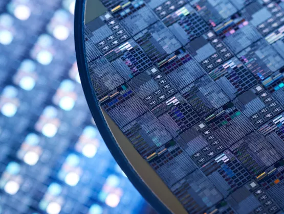
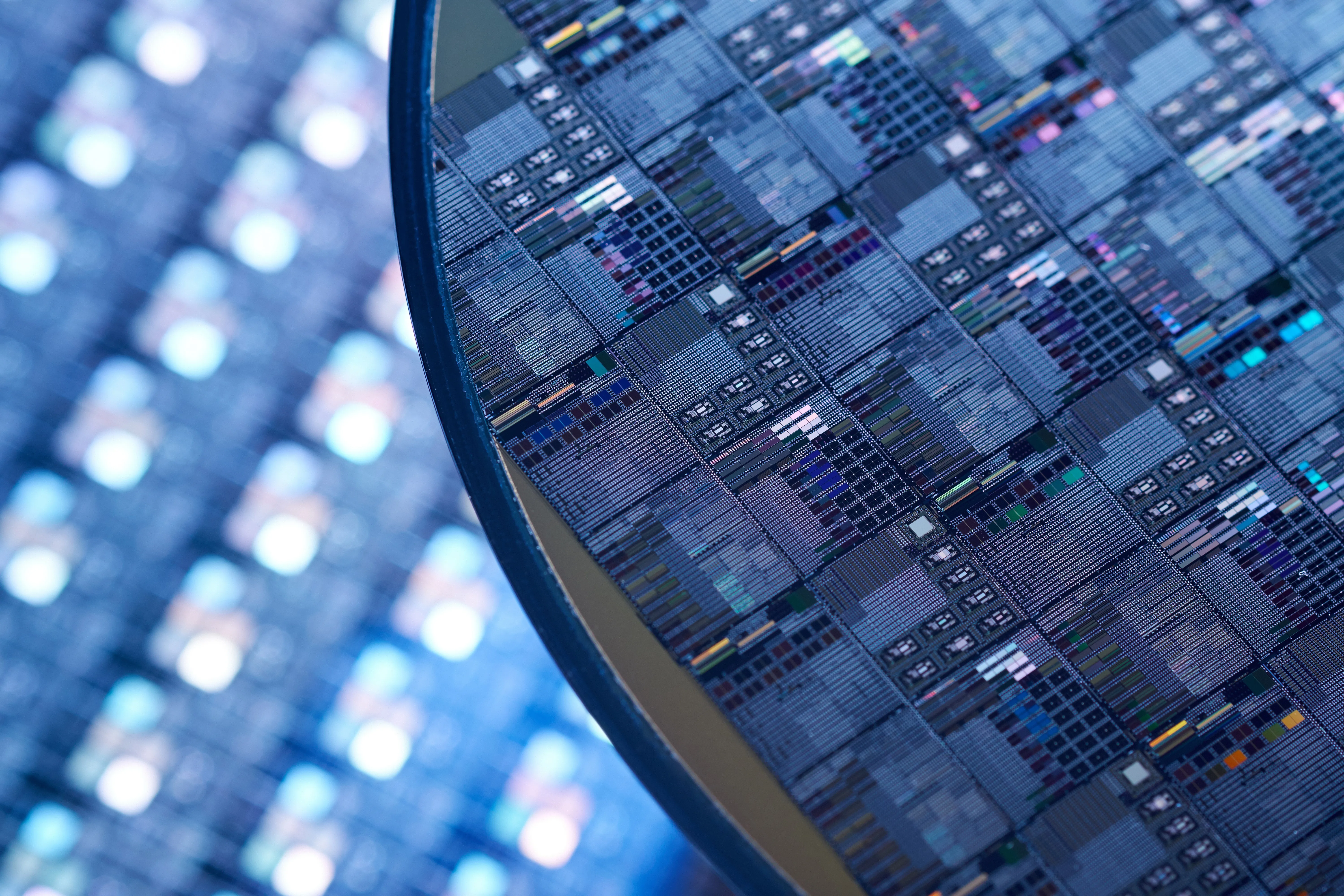
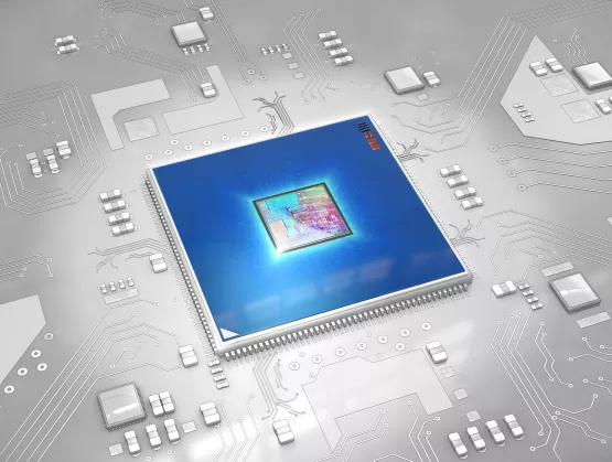
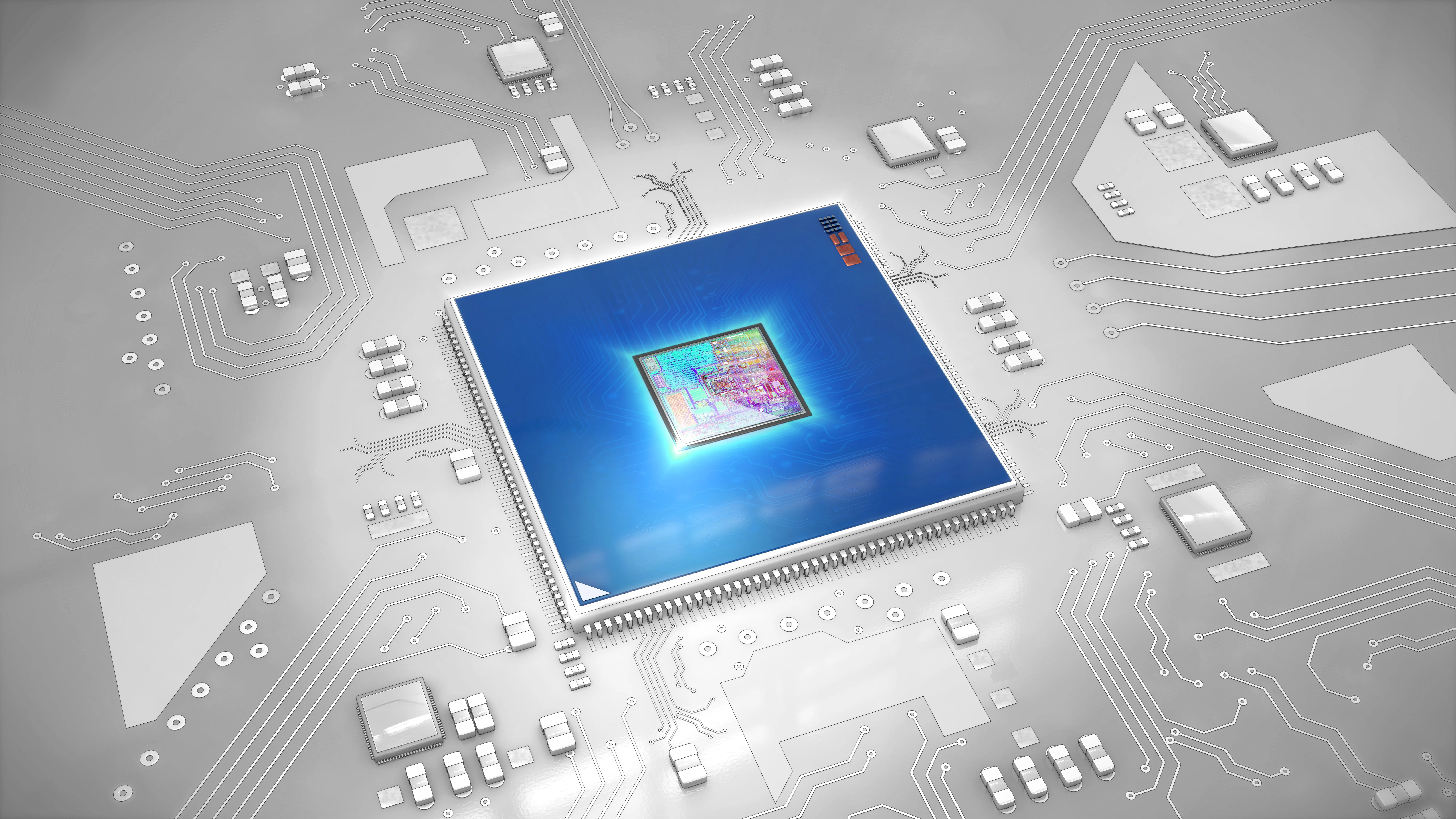
On May 8, a group of students gathered at SEMICON Southeast Asia for a one-of-a-kind experience. These students would be the first in the region to participate in SEMI High Tech U (HTU) – diving into the deep technology at the core of our industry. They simulated the layering process used in the wafer fabs for microelectronics and solar cell fabrication, then identified uses of integrated circuits and how the process evolves from materials (silicon) to product (patterned wafers).Nearby, another group of students jumped into lessons about gates and binary logic, the language of computers and how they communicate. They played with four basic logic gates – “AND”, “OR”, “NOT” and “XOR” – by using logic boards. Then it was high time to apply what they learned about gates and the binary systems – the inner workings of a calculator – and launch into the much-anticipated Human Calculator game. During the game, students become a 2-bit adder. First, they must convert numbers into binary and then trace the digits through a series of gates. It's only with careful communication and concentration that teams get the right outputs.HTU is the SEMI program that introduces students to science, engineering, technology, and math (STEM) through hands-on activities and experiential learning led by industry volunteers. Since 2002, HTU has reached some 8,000 students in 12 states and nine countries.Southeast Asia hosts first HTUThe ‘Human Calculators’ were one of two groups of more than 80 high-school students from four schools who came to the Malaysia International Trade and Exhibition Centre (MITEC) in Kuala Lumpur for a fun day of education and workshops. The sessions were led by instructors Shafiq Shahmeen and Zafryl-Zaheidy Mustofa from Inari-Amertron and Jamaludin Johar and Huichin Chew from STMicroelectronics.Kicking off the sessions, High Tech U program manager Bryson Gauff gave an oral history of HTU with the students and their teachers and prepped them for the exciting workshops.From India to the United States – Ajit Manocha’s inspiring storySEMI president and CEO Ajit Manocha, on stage for the ribbon-cutting to celebrate the Southeast Asia’s first HTU, shared the story of how he was moved to enter high technology at a young age. Growing up in New Delhi, India, Ajit developed his passion for engineering after being inspired by a close family friend. His love of bits and bytes led him to the United States, where he started his career at Bell Labs, working with semiconductors. Reflecting on his past, he told the students that if a young boy from New Delhi can become an engineer and move to the U.S. to pursue his dream, everyone in the room can do it too – whatever their passion. Much like his friend as a youth, Ajit paid it forward by encouraging the students to follow their hearts: “The future is yours and you can be whatever you want to be.” Ajit Manocha and Professor Madya were joined onstage by Kai Fai Ng, president of SEMI Southeast Asia, and Leslie Tugman, SEMI VP of Global Workforce Development and Diversity, for the ribbon-cutting at SEMI High Tech U in Southeast Asia. The power of experiential learning YBrs. Prof. Madya Dr. Wan Zuhainis Binti Saad, Director of Academic Development Management, Ministry of Education, lit up the room with her passion for education. She quickly connected with the students as she shared her story of being a microbiologist and a professor. She encouraged the students to learn together and do what they love. A strong advocate for empowering learners, Professor Madya also offered a transformational approach to teaching students in the 21st century education – a dynamic, forward-thinking mix of passion-based learning, experiential learning, and entrepreneurial innovation.She believes the more students blend STEM studies with other curriculum like the arts and humanities, the better they can work collaboratively and develop their passion in life. Professor Madya thrilled the roomful of students with her message about what the future holds for all students, especially those participating in Southeast Asia’s first-ever High Tech U.The future of electronicsWith today’s semiconductors processing data at blurring speeds, the program ended aptly with awards for quickness. The awards ceremony, sponsored by Edwards Technology Singapore, recognized the winning team for the fastest Human Calculator in each session. And all four schools received certificates for participating in High Tech U to celebrate the work of all the students – the faces of the future of electronics.SEMI welcomes Southeast Asia to the global High Tech U community! To learn more about SEMI HTU please visit our website. The first-ever SEMI HTU Southeast Asia students with their teachers, industry volunteers and HTU staff at SEMICON Southeast Asia. Ariana Raftopoulos is a marketing communications manager at SEMI.