downloadGroupGroupnoun_press release_995423_000000 copyGroupnoun_Feed_96767_000000Group 19noun_pictures_1817522_000000Member company iconResource item iconStore item iconGroup 19Group 19noun_Photo_2085192_000000 Copynoun_presentation_2096081_000000Group 19Group Copy 7noun_webinar_692730_000000Path
Skip to main content
In 2000, the average car sported 30 to 50 semiconductors. By 2025, the number of chips and sensors in an automobile will soar to an eye-popping 70,000 as it comes uber-connected and immeasurably smarter, powered by machine learning, artificial intelligence (AI), Internet of Things (IoT), visual sensing, high-precision mapping and other advanced capabilities.Today, the proliferation of semiconductors in cars is remaking the automotive industry as four major forces – electrification, connectivity, autonomous driving and diverse mobility – take hold, according to the consultancy firm McKinsey in its report Automotive Revolution – Perspective towards 2030 report. The chip industry saw auto-related sales jump from US$7 billion in 1995 to US$30 billion in 2015, a trajectory that has steepened over the past two years as major chip suppliers have rolled out products for precision mapping, navigation, in-car entertainment, and communications. With semiconductors fast becoming a major aspect of automotive design, traditional automakers are quickly moving to build strong partnerships with the semiconductor sector.Audi, a leading German car brand, took a big step to just that when it became the first automotive OEM to join SEMI as a member in June 2019 and strengthen the automaker’s ties to the semiconductor industry. With a massive market potential to tap, are Taiwan's auto electronics firms well-positioned to work even more closely with first-tier car brands like Audi?At the Smart Transportation Forum on September 18 at SEMICON Taiwan, Andre Blum, project manager at AUDI AG, will join Ian Chan, CTO of Cyntec, to offer insights into how automakers can team up with Taiwanese auto electronics companies. TechOrange, a Taiwanese tech news online media, spoke Blum ahead of the event about Audi's smart car efforts and the carmaker’s work to integrate new technologies into its automotive designs as it forms new partnerships with the semiconductor industry.Blum joined Audi in 2004 and since 2016 has led manifold projects within the group driving Audi’s work with semiconductor companies (Progressive Semiconductor Program). He has seen the automotive industry rapidly accelerate the integration of high technology in vehicles, an area where Audi excels. “The industry is changing how it works and new partners are joining the ecosystems," Blum said.Audi Wants to be the Next Apple in the Car SectorAudi's business developments in recent years echo Apple's early push to integrate the Internet and a panoply of applications into mobile phones. The difference now is Audi is working to integrate a wide range of smart applications into its automobiles for – ala Apple – the best user experience.For example, Audi has recently launched cars designed with Traffic Jam Pilot, Parking Pilot, and Garage Pilot three smart driver-assisting systems. With Traffic Jam Pilot, drivers no longer need to be on standby when stuck in the traffic. Instead, they can kill time with an infotainment system. While out shopping or making other stops, Parking Pilot helps drivers find a parking spot and park automatically. Garage Pilot provides a more comfortable parking-at-home experience – the driver waits maneuvers the car into the garage using handheld remote control. Audi stepped up its efforts in 2019 and revealed its latest concept car at the Shanghai Auto Show. Dubbed Audi AI:ME, the vehicle is equipped with a dizzying array of high tech: level-four self-driving technology, technology that allows the driver to control features with eye movements, LED units in headlights and taillights that change brightness accordingly at night and in bad weather, and VR goggles for onboard infotainment. Innovation and Tech Both Key to the New Driving ExperienceAutomotive technology is rapidly advancing in areas such as electric vehicles, autonomous driving and smart auto electronics. Cars of the future must have more computing power and connectivity to deliver a great user experience that includes high battery efficiency to extend the duration between recharges, in-car entertainment, and intelligent voice assistants – all capabilities made possible by semiconductors.Unburdened by the tasks of driving, passengers will enjoy a more intimate relationship with their vehicles. "The in-car entertainment system will allow passengers to have a teleconference or enjoy a movie in a theater-like setting,” Blum said. Switch on the self-driving system and you can drive through the night from Munich to Hamburg, covering a distance of 800 kilometers in the comfort of a home-like environment. The trip is even possible on one charge, meeting high energy-saving standards.These capabilities are technologically feasible now, but government regulations and policies still need to catch up. In the meantime, Blum says that Audi is focusing on creating a top-notch experience for car users today."The minute you step into a car, all the features, including the seat, radio channels, and the entertainment system will have already been adjusted to your liking and seamlessly connected to your mobile or other hand-held devices," he said.What does the Future Hold for Taiwan in the Next Blue Ocean Market?Semiconductors are the heart of these features, and Blum believes Taiwan is uniquely positioned to drive advances in automotive chips. Taiwan is home to semiconductor powerhouses TSMC and ASE as well as auto electronics companies, and its sophisticated mobile phone supply chain has endowed it with deep experience in integrating semiconductors with electronic modules – advantages that give Taiwan a head start in the automotive semiconductor market.Audi, too, is in a strong position to thrive in the new age of automotive electronics as it looks to its membership with SEMI to collaborate with companies across the microelectronics supply chain.“With rapid advances in automotive electronics technology, semiconductors now play a critical role in innovation and product differentiation,” said Dr. Klaus Buettner, executive vice president of Development Electrics/Electronics, CarIT, Audi.“To fulfill the promise of sustainable, connected-to-everything, highly automated mobility up to autonomous driving, we need to also align automotive requirements across the entire semiconductor value chain,” he said. “With its global platform, SEMI is the right association to bring together supply chain stakeholders for the close collaboration critical to driving technology innovation.”Emmy Yi is a marketing specialist at SEMI Taiwan.
Read More
As a top semiconductor manufacturing hub, Korea is poised to lead the world in fab construction spending in 2019 and 2020, accounting for 27 percent of the total market. Little wonder that Korea’s prowess in the semiconductor industry has meant steady membership growth for SEMI Korea, with HD Cho, president of SEMI Korea, putting the average annual jump at about 7 percent.But HD Cho’s focus as he returned to COEX in Seoul, home to SEMICON Korea, in late August was not on membership growth over the years but the future. Cho hosted about 400 SEMI members gathered at SEMI Korea Members Day for insights into the state of the world economy, semiconductor industry outlooks, and perspectives on how South Korean and European microelectronics companies can form stronger ties. Setting the stage with look at macroeconomics, Byung-yeon Kim, team manager of NH Investment and Securities, predicted that, as the global economy continues to falter, 25 of the 58 major countries this year will cut interest rates in a bid to boost prospects for growth. Historically, the global composite leading indicator (CLI), a bellwether for turning points in the economy, has rebounded after 20 months of decline, he said. While the CLI downtrend is now past the 20-month mark, Kim struck a bullish note, predicting that the global economy will bounce back before long.Soo-kyoum Kim, vice president at IDC, referring to the semiconductor industry’s own soft patch, said that total revenue is expected to drop from $475 billion in 2018 to $440 billion this year but should rebound to a new high of $500 billion in 2023. The memory market will be especially hard-hit, dropping more than 29 percent in 2019 and another 14 percent next year before bottoming and then staging a recovery in the second half of 2020. The strength of the rebound will hinge on server market demand, he added.Next year will also see rebounds in semiconductor equipment and materials revenue, with growth of 12 percent and 3 percent, respectively, said Clark Tseng, director of Industry Research and Statistics at SEMI. The increases will follow a 2019 equipment market drop of 18 percent to $53 billion from the previous year while materials this year is expected to remain flat at $52 billion. The semiconductor industry will expand at a modest 2.4 percent this year, jumping to 7.6 percent in 2020, Tseng reported, citing the average growth rate based on data from Gartner, WSTC, IC Insights, VLSI Research and other industry analyst firms. Despite current weak market demand and the ongoing trade war, the long-term outlook for the semiconductor industry remains upbeat, he added.In Europe, semiconductor industry growth continues on the strength of the region’s high strategic importance in the global electronics supply chain, said Laith Altimime, president of SEMI Europe. Fab construction spending in Europe continued to grow in 2018, reaching $300 million, and is expected to hit $1.2 billion in 2019 and $1.6 billion in 2020, with equipment, parts and components driving the surges.To help build stronger ties between European and Korean chip industries, Altimime introduced the SEMI Korea members to SEMI Europe business platforms including SEMICON Europe, the 3D System Summit, ISS Europe, and the MEMS Imaging Sensor Summit. He also encouraged the formation of more business partnerships between companies in the two regions by familiarizing SEMI Korea members with European players in areas such as foundry, MEMS, sensors and wafer manufacturing.And it will be MEMS and sensors that help drive the 4th Industrial Revolution, said Sung-hyuk Kim, a team leader at LG Electronics' Sensor Solution Research Institute. In his presentation Architecting Sensor Solutions for the Next Revolution, he noted that sensors are finding their way into devices where they have never been used before. In household refrigerators, gas sensors help deodorize the inside while distance sensors detect the approach of people. Air conditioners equipped with a camera sensor can pinpoint the location of humans and steer the airflow in their direction. Of course, all these smarts will come in form of data-devouring artificial intelligence (AI), and that data will be generated in massive amounts by MEMS and sensors – placing them at the epicenter of the 4th Industrial Revolution.Jaegwan Shim is a marketing specialist at SEMI Korea.
Read More
SEMI spoke with Dr. Mikko Söderlund, sales director for Beneq’s semiconductor business, about trends in Atomic Layer Deposition (ALD) applications. Söderlund shared his views ahead of his presentation at SEMI MEMS Imaging Sensors Summit, 25-27 September, 2019, at the WTC in Grenoble, France. Join us at the event to meet Beneq and other key industry influencers. Registration is open.SEMI: The Backside Illuminated (BSI) CMOS Image Sensors (CIS) market continues to experience steady growth. Which applications are currently driving market growth?Söderlund: BSI CMOS Image Sensor market continues to be driven by mobile, security, automotive and Internet of Things (IoT) applications – so there seems to be plenty of opportunities for BSI CIS market to grow further.SEMI: What is critical for advanced thin-film deposition methods to extract best electrical performance?Söderlund: It is critical to control the material properties of the deposited layer (such as charge density, resistivity or barrier property) and of course, film uniformity and conformality. Furthermore, controlling material interfaces is also important, especially for sensitive III-V materials. {% video_player "embed_player" overrideable=False, type='scriptV4', hide_playlist=True, viral_sharing=False, embed_button=False, width='350', height='197', player_id='12721134435', style='margin: 0px auto; display: block; float: right; margin-left: auto; margin-right: auto; width: 350px;' %} Coatings and material features based on existing standard techniques can be very expensive, or not feasible at all. What does Atomic Layer Deposition (ALD), as a thin film coating method, offer in particular?Söderlund: ALD offers dense, highly conformal and pinhole-free best-in-class functional layers for dielectrics, passivation, encapsulation and much more. As a gentle and precise layer-by-layer method, ALD is extremely well-suited for deposition of such performance critical layers over large surface areas such as a cassette of wafers.SEMI: Please describe the Atomic Layer Deposition (ALD) coating process. Söderlund: ALD is based on a self-limiting surface reaction controlled thin film deposition. During coating, two or more chemical vapors or gaseous precursors react sequentially on the substrate surface, producing a solid thin film (see schematic below). Most ALD coating systems use a flow-through traveling wave setup, where an inert carrier gas flows through the system and precursors are injected as very short pulses into this carrier flow. The carrier gas flow takes the precursor pulses as sequential waves through the reaction chamber, followed by a pumping line, filtering systems and, eventually, a vacuum pump.SEMI: What are the two leading edge ALD applications?Söderlund: Today’s leading-edge ALD applications are in logic (high-k/metal gate, multiple patterning) and memory (DRAM capacitor, 3D NAND). Within the More-than-Moore (MtM) markets, CIS and MEMS (actuators and sensors, RF) have been early adopters of ALD, and we also see ALD being introduced in GaN Power and RF, as well as photonics.SEMI: Give us one prediction about the opportunities offered by advanced imaging applications.Söderlund: The large diversity of imaging applications will continue to drive growth and innovation. For example, machine vision is expected to transform the imaging landscape. We see this as a big opportunity for advanced thin-film deposition methods such as ALD, provided that the tools are versatile enough to address the diverse manufacturing requirements.SEMI: What are your expectations for SEMI MEMS Imaging Sensors Summit and why do you invite your peers to attend? Söderlund: The summit brings together all key RF stakeholders in the MEMS and imaging sensors industry, and we are looking forward to a great event. It’s a special event for us as we are officially launching a new ALD cluster tool product specifically engineered for the MtM applications – so this brings great excitement that we want to share with the attendees.Dr. Mikko Söderlund is Sales Director for Beneq’s semiconductor business. He has more than 20 years of experience in product development, product management, technical sales and business development across the photonics, OLED, and semiconductor industries. Mikko received his Ph.D. in Micro- and Nanotechnology from the Helsinki University of Technology. Serena Brischetto is a marketing and communications manager at SEMI Europe.
Read More
The BioMEMS market is becoming increasingly diverse, encompassing gas and pressure sensors, ultrasound, specialized biomedical sensors, and other types of MEMS and microfluidic chips used for drug delivery and analytical applications. The BioMEMS market is also growing steadily: Research firm Yole Développement predicts that BioMEMS will grow at 14.9% CAGR from 2017-2023, reaching US$6.9B by 2023.1 As a high-value market, BioMEMS is worth pursuing as long as you can manage the complexities of manufacturing, including a sometimes-fragmented supply chain. Fortunately, the MEMS manufacturing ecosystem is evolving to accommodate the needs of companies that are in the process of commercializing BioMEMS-enabled products. Understanding the ecosystem’s shifting dynamics will help BioMEMS to flourish in this promising while often-challenging market segment.Unique Product, Unique ProcessIn the world of semiconductor manufacturing, it is routine for a fab to manufacture hundreds of different device designs using just a handful of process nodes. Semiconductor foundries share their design rules with customers, who then develop the mask set accordingly, literally adapting their designs to fit the rules for manufacturing on one of the foundries’ process nodes. In stark contrast, most MEMS devices cannot conform to the level of standardized manufacturing processes that work so well for semiconductors. Rather, MEMS challenges us to develop individualized processes for each device. It’s one product, one process.New BioMEMS designs generally emerge from either corporate R D or academia, two groups that approach specialized MEMS foundries such as ours when they’re entering pilot or low-volume production. Today successful commercialization depends on open, accurate communication and close collaboration. MEMS foundries must work side-by-side with designers to ensure that designs are based on real-world manufacturing process technologies. This highly customized manufacturing model makes it very difficult to support future demand for the groundswell of diverse BioMEMS devices that are in development. If we want to handle this upward trajectory of BioMEMS, we’ll need to adapt.Change the ModelWhile most existing MEMS foundries currently support a wide variety of devices types, I predict that market forces will cause our foundries to move toward specialization. Some companies will specialize in what they already do best, e.g., inertial sensors for the automotive industry. Others might choose to develop their foundry business around a purpose-built facility, which, for example, only manufactures microfluidics or magnetic devices. Larger enterprises might opt to build captive foundries that are designed to serve their specific needs. Get Creative: Combine, CollaborateSatisfying the thriving market for BioMEMS will require creativity. One idea: combine different disciplines of the manufacturing process at the same foundry. For example, we could have a biochemistry fab and a MEMS fab under the same roof, or we could have a MEMS fab and a packaging facility in one building. While these approaches may not yet exist outside of academia, necessity may drive them to fruition.It will also require heightened strategic collaboration, a process that has already begun. To support both large volumes and greater diversity of devices, some MEMS foundries are building cooperative relationships with former competitors. Think of it as a restructuring of the supply chain.Embracing the special challenges of BioMEMS manufacturing is worth our investment in time and resources. We need to step back, individually and collectively, to understand where each of the existing MEMS foundries fits into the new supply chain so we can leverage our strengths. We can start by forging stronger alliances for tech transfer. Once we more freely share information as we engage in joint product development — involving technology teams who are more connected and less guarded — we will expedite tech transfer and manufacturability.While we are unlikely to achieve the same level of standardization that has enabled the semiconductor industry to reach its great heights, as long as we evolve to meet demand, we will grow together and prosper.To learn more about this topic, meet with Jessica Gomez at the upcoming SEMI-MSIG MEMS Sensors Executive Congress (October 22-24, 2019 in Coronado, Calif.) or email her: [email protected][1] “BioMEMS Emerging Non-Invasive Biosensors: Microsystems for Life Sciences Healthcare 2018 Report,” Yole Développement, https://yole-i-micronews-com.osu.eu-west-2.outscale.com/uploads/2018/08/Sample-BioMEMS-Non-Invasive-Sensors-Microsystems-for-Life-Sciences-Healthcare-2018-.pdf As founder and CEO of Rogue Valley Microdevices, Jessica Gomez has created a world-class precision MEMS foundry and wafer fab in the heart of Southern Oregon. Integral to her role as CEO, Ms. Gomez practices a business philosophy of offering custom design, best-in-class process technology and R D expertise to customers, to help them achieve the highest quality and reliability in their products.In 2018, Ms. Gomez was selected for the prestigious SEMI Board of Industry Leaders. SEMI also recognized her in its first Spotlight on SEMI Women, which honors accomplished women in the global microelectronics industry.Prior to founding Rogue Valley Microdevices in 2003, Ms. Gomez honed her experience in semiconductor processing and production management through positions at Standard Microsystems Corporation, Integrated Micromachines and Xponent Photonics.For more information, visit: https://roguevalleymicrodevices.com/Rogue Valley Microdevices is a longtime member and supporter of SEMI-MEMS Sensors Industry Group, which connects the MEMS and sensors supply network, allowing members to address common industry challenges and explore new markets.
Read More
Automotive original equipment manufacturers (OEMs) and their direct suppliers of parts and systems share a vision: Next-generation vehicles will be more electric, autonomous and connected. At a market size of more than $1 trillion, automotive is steadily becoming a high-tech market as cars morph into advanced technology platforms with partially or fully autonomous features. Call them semiconductors on wheels. Big players such as Google and many carmakers are investing heavily in chip advances to help drive increases in silicon content in automobiles.At SEMICON Europa, Pierrick Boulay, Solid State Lighting and Lighting Systems analyst at Yole Développement, will provide a market update on autonomous automobile trends including the state of sensors, radars, cameras and LiDARs as the industry works to increase the level of autonomy and electrification.Autonomous vehicle design can only thrive with the development of an industry standard for chip and device traceability across the supply chain. The importance of chip traceability to the automotive industry is reflected in its central role in driving a chip traceability standard.According to Heidi Hoffman, senior director of technology communities marketing at SEMI, “chip traceability is one of the next big things for the technology industry. The benefits are enormous, and the upsides – including yield enhancements, counterfeiting safeguards, and support for new applications – are plentiful. But the implementation challenges of chip traceability are also big and will require considerable effort to overcome. The biggest hurdle of all? We need to transcend industry fears by demonstrating that we can secure IP when it is shared across the hardware supply chain.” The Importance of Standards, Data Collection and Collaboration Across the Supply ChainThe automotive industry has long embraced tracing the sources of defects. Now, as the automotive and semiconductor supply chains increasingly overlap, traceability has taken on greater importance in the semiconductor industry. SEMI committees, task forces and events such as the Smart Transportation Forum at SEMICON Europa are ideal platforms for collaborating to develop new standards and best practices for the automotive industry.Earlier this year, German luxury automobile maker Audi AG became the first automotive original equipment manufacturer (OEM) to join SEMI as member, strengthening alignment across automotive supply-chain segments. At SEMICON Europa, the SMART Transportation Forum and Pavilion, staged by the SEMI Global Automotive Advisory Council (GAAC) and bolstered by the Electronic System Design Alliance, a SEMI Strategic Association Partner, will gather key stakeholders across the automotive value chain, from design and semiconductor equipment to materials and carmakers, to explore innovation opportunities in automotive electronics. SEMI Global Automotive Advisory Council (GAAC) “If the industry wants to reach the goal of zero defects, a new collaborative approach is necessary,” observed Antoine Amade, senior regional director EMEA at Entegris. At SEMICON Europa, Amade will present new ways to collaborate in reducing chip defectivity and meet other challenges in the automotive industry.More than half of semiconductor failures on the automotive assembly line today (so-called 0km failures) are traced to semiconductor fab defectivity. “The increasing semiconductor content in automobiles – driven by growth in ADAS, electrification and autonomy – has put a growing focus on the quality and reliability of these devices and their implications for consumer safety and satisfaction,” said Oreste Donzella, senior vice president and CMO at KLA.The smart manufacturing (Industry 4.0) revolution is already spurring higher performance and great efficiencies throughout the supply chain and will also be crucial to driving innovation in automotive. Smart manufacturing makes possible significant improvements in factory key performance indicators (KPI) for cycle time, on-time delivery, overall equipment effectiveness, cost and product quality.“These KPI gains are key to meeting quality levels the automotive industry must reach to support the deployment of autonomous driving vehicles,” said John R. Behnke, general manager of Final Phase Systems at INFICON. In his talk at SEMICON Europa, Behnke will provide an overview of existing, in-progress, and future smart manufacturing solutions for the semiconductor industry and their impact on the automotive supply chain. The SMART Transportation Forum, 13 November, 2019 (9:30-15:30 at ICM Munich, room 14c) at SEMICON Europa is the premier platform for key stakeholders to connect, collaborate and innovate across the automotive value chain. Automotive and semiconductor industry experts will offer insights into trends in design, semiconductor equipment and materials, and automotive innovation and the roadmap to 2030. The SMART Transportation Forum will also showcase innovations in imaging, sensing, artificial intelligence (AI), smart manufacturing and L5 mobility.Other SEMICON Europa highlights: Advanced Packaging Conference: Packaging and Test Challenges Towards High Reliability (12-13 November 2019) 23rd Fab Management Forum: Game Changers for Semiconductor Operations(11-12 November 2019) Strategic Materials Conference: Strategic Materials Enabling Industry Roadmaps(12-13 November 2019) SEMICON Europa registration is open for visitors and exhibitors. For more details, please visit the SEMICON Europa website and connect with SEMI Europe on Twitter or LinkedIn @SEMIEurope (use #SEMICONEuropa).Learn more about the SEMI chip traceability standard – SEMI T23 - Specification for Single Device Traceability for the Supply Chain – and SEMI Technology Communities.Serena Brischetto is a marketing and communications manager at SEMI Europe.
Read More
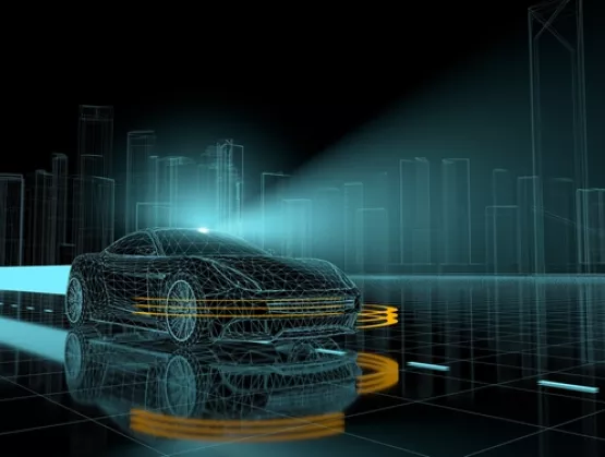
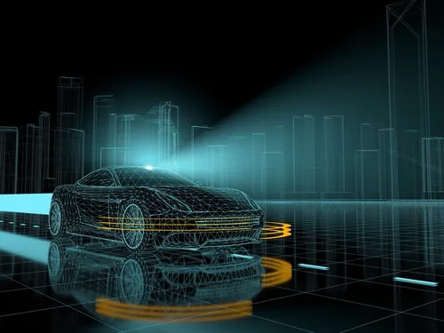
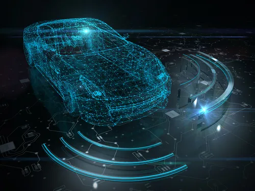
Stefano Zanella, Head of Automotive, Industrial and Location Businesses, TDK InvenSense will present at next month’s SEMICON Taiwan (September 18-20, 2019 in Taipei City, Taiwan). SEMI Taiwan’s Emmy Yi spoke with Stefano for a preview of his talk.SEMI: What macro market trends are driving automotive manufacturers to increase the variety and volume of MEMS sensors in cars?Zanella: The car world is changing. Consumers increasingly view car ownership as less desirable, yet the number of miles traveled and of hours spent in a car are rising steadily. At the same time, cars are changing profoundly, and the pace of change is rapid. To thrive in this new world, automakers are becoming transportation enablers and providers.Many vehicles today autonomously interact with humans and the world around them, operate with less or no human control, and are powered by electric batteries. MEMS sensors – which mimic and augment the five human senses – are front and center in these advancements.Unlike other types of sensors – such as cameras, radar and GNSS/GPSS – MEMS gyroscopes are functional in every environment. Gyroscopes, as well as accelerometers, can supplement those other sensors when they are not available and boost the accuracy of their outputs when they are available. Both camera stabilization and dead reckoning when GNSS is unavailable are good examples of the latter. Other prevalent sensors include MEMS microphones, used to capture voice commands, ultrasonic sensors, which can be leveraged for parking and gesture recognition, and fingerprint sensors, which can improve car security.SEMI: How can automakers stay competitive in this changing landscape?Zanella: Automakers can future-proof their relevance in the transportation market in several ways. By embracing consumer migration toward ride-sharing over car ownership, many are transforming from manufacturers to mobility providers. Carmakers that invest in ride-sharing and other modes of transportation (e.g., scooters) can sustain their profitability, even if the number of vehicles sold eventually shrinks or simply doesn’t grow as much as anticipated.Automakers will need to pursue new avenues of product differentiation. Traditionally, automakers have kept performance and aesthetics to themselves by owning the engine and the body design of the car, leaving nearly everything else to suppliers. Autonomous driving and electrification, however, are pushing automakers to own the battery pack and the autonomous driving software stack.While we are just beginning to see standardization in battery packs, automakers are likely to own the autonomous driving stack for many years to come. Automakers that offer cars with highly functional and efficient batteries and driving stacks stand to gain market share.Automotive infotainment systems will become increasingly crucial as autonomous driving turns everyone into a passenger. Audio subsystem providers such as Harman Kardon, Bose, and Bang Olufsen, for example, jockeyed for attention at the most recent Geneva Motor Show, demonstrating sophisticated surround-sound systems that rival premium-quality home audio setups.With more and more consumers using voice interfaces to interact with devices in the home, drivers are less willing to accept spotty accuracy in the car. Hence, automakers are using more higher-performing MEMS microphones to accurately capture voice commands. This will come as a relief to those of us who routinely yell at our steering wheels while using voice command to try to call home. Demand for higher quality infotainment systems has prompted some automotive OEMs to own the entire infotainment system and work directly with sensor and chipmakers, a level of intimacy that gives automakers a chance to tune sensor and chip development to their own needs. This tighter relationship also positions device suppliers to forge more direct links with drivers.SEMI: Which MEMS sensors are particularly important to tomorrow’s automobiles and why?Zanella: For many years the automotive industry has been integrating more electronics into cars to improve safety, advance the driver and passenger experience, and, more recently, power the car. As vehicles rely less on human control, automakers must replace the senses of the driver with something else. That something else is a bunch of sensors, microphones, cameras, radar and LIDAR to replace vision and hearing.Since MEMS sensors such as accelerometers, gyroscopes and pressure sensors are much more robust than other types of sensors to operate in snow, rain and darkness and other imperfect environments, automakers use them to ensure that the vehicle never gets lost when other sensors and/or the GPS/GNSS signal become unavailable in tunnels or urban canyons. Gyros help determine direction, accelerometers velocity and distance driven, and pressure sensors height, such as when taking a fork on a multi-level highway. At the same time, fingerprint sensors, ultrasonic parking sensors, and temperature sensors are improving convenience, safety and security for the car’s occupants. Automakers increasingly use inertial and environmental sensors, MEMS microphones, fingerprint sensors, and vision/imaging sensors to augment or replace the five human senses on which car drivers have relied for over 100 years. Source: TDK InvenSense SEMI: To what degree can MEMS sensors enable automotive security?Zanella: MEMS sensors are used widely to enhance security today. Some of their mechanisms are easy to understand while some are unexpected. For instance, ultrasonic fingerprint sensors can authenticate the driver of a vehicle to prevent car theft or something less onerous, like a teenage driver taking the car out without permission.Accelerometers and gyroscopes can prevent a new type of spoof on keyless entry systems. Imagine that you are very close to your vehicle. Your car senses the remote control in your pocket and automatically opens the doors when you pull the handle. Now suppose that your car is parked on the street, not far from your house. You leave the remote control home, and the car doesn’t sense the proximity of the remote control. Great! No one can enter your car, unless ... a thief has a big signal amplifier that makes your car think that the keyless entry device is next to the car. In this case, what can an automaker do? Add an accelerometer that restricts the keyless device from broadcasting the entry signal unless you are walking to the car with the device on your person.SEMI: What would you like SEMICON Taiwan attendees to take away from your presentation?Zanella: I would like them to embrace the transformations afoot in the automotive market as well as their associated design challenges since, by overcoming these hurdles, they can offer significant societal benefits such as safer and cleaner transportation. At the same time, these transformations mean significant opportunities for semiconductor industry revenue growth. And while design-to-delivery cycles in automotive are longer than in consumer and mobile, the automotive market supports higher-value devices as well as the chance to fold dozens of MEMS sensors into a single model.To paraphrase Lord Kelvin: If you can’t sense it, you can’t manage it. As suppliers of many key technologies that make intelligent transportation possible, the MEMS sensors industry is in an excellent position to help automakers manage the many challenges ahead.Stefano Zanella, Ph.D., is Head of Automotive, Industrial and Location Businesses at TDK InvenSense, where he brings MEMS sensors (including accelerometers, gyroscopes and microphones) and location solutions to the automotive and industrial markets. Zanella holds an MS and a Ph.D. in Electrical Engineering from the University of Padova, Padova, Italy as well as MBAs from both the UC Berkeley Haas School of Business and from Columbia University.He will present MEMS Sensors Enabling the Smart Car Revolution on Wednesday, September 18, 2019, at SEMICON Taiwan at 1F 4F, Taipei Nangang Exhibition Center, Taipei City, Taiwan. Register today and save 20% to learn how MEMS sensors are transforming the human experience with cars.Connect with Stefano Zanella at SEMICON Taiwan or via LinkedIn. You can also get more information on TDK’s automotive solutions and application guides online.Interested in engaging with the MEMS sensors supply chain? SEMI MEMS Sensors Industry Group is a technology community that enables professionals in the MEMS and sensors industry to innovate, address common challenges and accelerate business results.Emmy Yi is a marketing specialist at SEMI Taiwan.
Read More
The future of the semiconductor industry began to blossom recently in Seoul, South Korea as young, innovative minds teased out secrets to electronics manufacturing and their path to enter the industry one day. Twenty-seven middle schoolers gathered in early August at Yonsei University for SEMI High Tech U (HTU), the worldwide SEMI program that introduces students to science, engineering, technology and math (STEM) careers over three days of hands-on activities and experiential learning. Since 2001, HTU has reached some 8,000 students in nine countries.Semiconductor giants including Applied Materials, KLA, Lam Research and Dongjin Semichem were key teachers as representatives from the companies gave theoretical and practical lectures to pique the students’ interest in STEM educations and careers. The speakers, all experts in microelectronics, surveyed microchips and solar cells, mathematical and scientific experimentation, engineering design and the inner workings of semiconductor manufacturing before the students broke off into teams for lessons largely of their own making. Fine-tuning a wooden contraption – a Statapult – to hurl a ball as far as possible might not sound like the stuff of microelectronics, but it drew on the type of problem-solving skills and creativity the students will need to thrive in the semiconductor industry. Student teams made adjustments to the levers of miniature catapults, then tested the throwing power of the devices. After the ball tosses, they reconvened as a class to share lessons in how they calibrated their catapults for a longer tossing distance and ways they could improve the devices’ performance. Students also took tours of two very different semiconductor manufacturing settings – one virtual and the other real. The young learners donned virtual reality headsets for a simulated walk-through of Applied Materials (the tour was sponsored by the company), then slipped on bunny suits for a tour of Yonsei University's BIT micro fab and a close-up look of how semiconductors are made.But it was the ever-popular Human Calculator game that inspired the greatest thrill as students dove deep into technology. During the exercise, they converted numbers into binary and then traced the digits through a series of gates in an electronic circuit, an exercise requiring careful team communication and concentration to generate the right outputs. The students surprised SEMI Korea employees and instructors, and themselves, by completing the exercise with record speed. Their time: less than two seconds.Human resources managers from sponsor companies were on hand to give the middle school students a head start in their careers with lessons in resume writing and career management. In mock interviews, the students honed their interviewing skills. And in meetings with SEMI High Tech U alumni they learned how their predecessors worked their way into semiconductor industry and their focus of study in college.To be sure, the day was rich in details about working in the microelectronics industry. But did it meet the students’ expectations? In a survey before the event, the more than two dozen students, on average, rated their knowledge of microelectronics at 4.5 on a scale of 1 to 10, a score that jumped to 7.7 after completing HTU. Their favorite module? No surprise: Engineering Design. In this exercise, the students designed a carrier for six 12-ounce beverage cans using only decidedly low-tech materials such as strings, rubber bands and wooden boards. Their innovations were studies in high creativity and ingenuity – just the type of imaginations the semiconductor industry needs. SEMI Korea has offered SEMI HTU since 2011. This year, various other career development programs such as semiconductor manufacturing tutorials and mentoring are planned as SEMI Korea continues to sow the seeds of the next generation of industry workers. Jaegwan Shim is a marketing specialist at SEMI Korea.
Read More
This article is the fifth and final in a series highlighting the vital importance of SEMI Standards to commemorate the publication of the 1000th SEMI Standard in July 2019. Find the entire series here.As we define industry standards for managing data in the fab and beyond, we are creating a virtuous circle. More data create better processes. Better processes generate more good data, and more good data lead to better processes. It becomes a cycle of continuous improvement, and we are only just beginning to realize its potential. To dive deeper we interviewed Alan Weber, vice president, New Product Innovations at Cimetrix, and an active member of SEMI Standards Information and Control Committee (IC C).“Industry standards are critical in allowing us to collect information across the fab and use it in increasingly sophisticated control algorithms for the equipment,” said Weber. “The last few years have been about analysis applications that leverage big data in the fab. What started at the lot level is now applied at the wafer level, and for a process like lithography, it’s down to the shot or die level. We’re now collecting enough data variables at individual process and recipe steps to model for predictive maintenance and virtual metrology.”The migration from using data as rearview mirror for identifying and addressing fab issues to using data to head off issues preemptively represents a paradigm shift with immense advantages. This is the starting point for realizing a virtuous data circle.The benefits of a virtuous data circle are simple and compelling: higher yields, faster time to market, more revenue and greater profitability. Our optimism, however, is tempered by major obstacles to this promising future.Multilingual ManufacturingWeber points out that the electronics industry is becoming a multilingual standards world with more than 1,000 fab equipment vendors and several layers of protocols that present the challenge of seamlessly handling multiple protocols. His IC C Committee is out to tackle this challenge.“While SEMI Standards efforts first began in the front end, our standards program now encompasses the back end with test and packaging as well as other device areas including MEMS, sensors and displays,” said James Amano, senior director, International Standards and EHS, SEMI. “We’re going to see data connectivity from the front end to the back end to the final assembly of multi-chip products and that needs standards,” Weber explained. “We’ll need more connected equipment throughout the global, multi-site manufacturing process if we are to support the full traceability requirements of the most demanding markets such as automotive.”The industry will benefit from greater collaboration. Weber predicts that companies will team to create integrated supply chains within broader industry supply chains.Getting the Right People at the Right Time“As we lead the development cycle of a standard from concept to realization, one of the most important jobs of our standards task forces and committees is to coordinate competing companies and build an industry consensus,” Amano said. “This is the case for data in particular, where we rely on industry professionals like Weber and his colleagues, who are working to bring people together to collaborate on developing standards for connectivity and data sharing. It is that critical human element that allows SEMI to sustain our commitment to introducing standards that move the industry forward.”Will Companies Share Data If It Is Secure? Weber contends that when it comes to securing and sharing the data, the biggest challenge is to change the industry’s information-sharing culture.“Finance and defense are already finding ways to deal with data security,” said Weber. “While we will always have problems that require technology fixes, like dealing with new types of computer viruses, I am confident that we will be able to create standards that enable the free, secure flow of information. The key to making progress and better leveraging data is to get companies to see the potential of sharing data while investing in the standards.”SEMI recently launched a project to optimize data sharing across two critical process steps – lithography and plasma etch – to accelerate the adoption of data-driven AI methodologies. The results will help to establish data transfer and management standards crucial to the trusted exchange of trade secrets, IP and other sensitive information. Tools and materials from several SEMI members will be used for the project at Cornell University’s NanoScale Science Technology Facility (CNF). SEMI members are invited to join the project review team. Contact Pushkar Apte at SEMI ([email protected]) for more information on the initiative.Advantages Are Too Great to IgnoreTraditional cultural obstacles aside, the advantages of creating virtuous data circles are simply too great to ignore. Now that it’s accepted wisdom for fabs, factories and supply chains to continuously leverage interconnected data to get smarter, the time has come to extend those advantages throughout the full manufacturing process. Without these data circles, we’ll slow the development of new technologies and applications.We can only speculate where the lines of sharing data are drawn and will be redrawn in the future. But, without doubt, technology innovations such as AI will spawn new information business models that vertically and horizontally integrate companies in ways previously unimaginable. Data standards will underpin this structural transformation.Use your voice to affect standardization in and around the microelectronics industry. Learn about SEMI International Standards – and become part of the solution. Heidi Hoffman is senior director of technology communities marketing at SEMI. Hoffman and her team shine a spotlight on the work of the more than 20 technology communities under the SEMI electronics manufacturing supply chain collaboration platform. Actively engaging community members in marketing programs that showcase their unique value, Hoffman’s team helps companies to grow and prosper through the power of connection, collaboration and innovation.
Read More