downloadGroupGroupnoun_press release_995423_000000 copyGroupnoun_Feed_96767_000000Group 19noun_pictures_1817522_000000Member company iconResource item iconStore item iconGroup 19Group 19noun_Photo_2085192_000000 Copynoun_presentation_2096081_000000Group 19Group Copy 7noun_webinar_692730_000000Path
Skip to main content
Why FD-SOI? What can you do with it that you couldn’t do before? That was the big question from IHS Markit’s Matthew Short that kicked off the first panel discussion at the SOI Consortium’s Silicon Valley Symposium. And there were some great answers.VeriSilicon, Analog Bits and Silicon Catalyst were among the consortium members with stands at the SOI Symposium, Silicon Valley 2019.Here in this final part of our coverage of the event, we’ll detail who said what in the two panel discussions, as well as the presentations by Leti, Intento Design the SOI Consortium’s IP/EDA roundup.If you missed the previous two installments of our coverage, you can catch up on the rest of the presentations in part 1 (NXP, Samsung more) here and part 2 here (Synaptics, GlobalFoundries more). Almost all of the presentations are now freely available under "events" on the consortium website - or just click here to get them.How FD-SOI Changes 
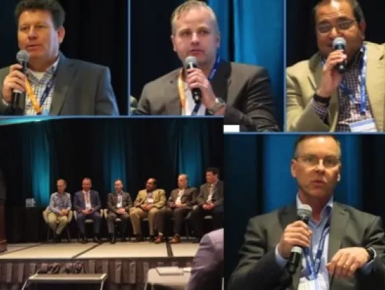
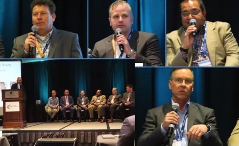
What You Can DoThe presentation by Matthew Short, Sr. Director of IoT Technology at IHS Markit, was not specific to SOI, but it sure did lay out out the market opportunities. Entitled IoT, 5G, ADAS and AI Market, it’s available on our website. Matt spent most of his career in chip design at NXP/Freescale, so he really has an engineer’s perspective on where this all is going. At IHS Markit, they define IoT as anything with an IP address. Over the past year more than 10 billion devices were shipped, and there were more “things” than cellular handsets, so the world has really changed. He outlined the growth drivers, suggested that 5G won’t be a “wow” thing for consumers, and noted there is a lot of debate raging regarding how smart sensors should be (the Tier 1’s want smart).He was then joined on the stage by the participants in the first panel discussion, which looked at product and application drivers. That included: NXP Fellow Rob Cosaro; Tim Dry, Director of Edge Endpoints Marketing at Samsung Foundry; ST biz dev director Roger Forchhammer; CoreAVI biz dev VP Lee Melatti; Nokia VP Michael Reiha; and Analog Bits EVP Mahesh Tirupattur.First Short asked why customers wanted more integrated solutions. For CoreAvi, it’s about safety, for ST in automotive it’s about security, for Analog Bits, it’s about integrating more analog, for Nokia it’s just a necessity.Then he asked Why FD-SOI? What can you do that you couldn’t do before? For ST, which is doing MCUs for automotive, it’s about energy efficiency, speed, the density of non-volatile memory and the robustness of the technology. For NXP, it’s back biasing, low voltage and power numbers never seen before. “FD-SOI really makes a difference in the products we can bring to market,” said Cosaro. For CoreAVI, it’s the long-term power impact. And for Analog Bits, “Customers see huge benefits,” said Tirupattur, for cost sensitive applications. He has customers selling their technology in high volumes in FD-SOI. What about edge vs. cloud? For Nokia, it’s monolithic integration for best-in-class RF, advanced memory, biasing and voltage regulation adding a layer of intelligence. Samsung sees edge as distributed cloud, and CoreAVI sees safety in the edge, because you can’t completely rely on the cloud.Where are the weak points in the FD-SOI ecosystem? For Samsung, more people need to use back biasing. “People need to use the knobs,” said Dry. For Analog Bits, the next step is innovation around back biasing, as many in logic don’t understand the benefits, so the ecosystem needs to promote the value proposition. ST suggests that with more products out there, customers will see the benefits. NXP did “a lot of the heavy lifting” at 28nm – now you need more people using these nodes, not just the cellphone nodes.How will the architecture change? For NXP, it’s all about memory bandwidth. For Samsung, it’s the promise of analog and interconnect. Nokia sees the back-end and heterogeneous integration with FD-SOI and RF enablement. Analog Bits’ Tirupattur said he’s pushing his engineers for even lower power in a still smaller form factor, noting that most analog engineers had been more focused on performance than power, but now that’s changed. For ST, it’s AI/ML throughout automotive, and 
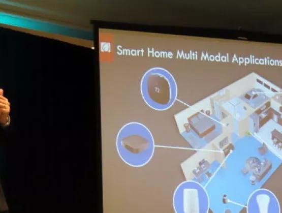
FD-SOI is beneficial there.Leti the Connected Car Leti's slide 27, SOI Symposium, Silicon Valley 2019Research giant Leti’s presentation was entitled Applications Around the Connected Car. 85% of Leti’s €315M budget comes from R D contracts with its 350 industrial partners. Truly a driving force in FD-SOI, Leti is involved in a dizzying array of projects. For the connected car, they cover (much of it on SOI): high precision smart sensing, embedded processing fusion, new computing paradigms and deep learning, ultra-low power computing nodes framework, ultra-low power connectivity for IoT, energy management and scavenging, and security. They do vision at the edge, 3D technology for smart imagers, and ways to dramatically reduce power. They’ve got a Qbits platform on FD-SOI for AI at the edge, a super low power neural network accelerator, and ULP connectivity. Check out the presentation for lots of details.EDA/IP OverviewSlide 9 from SOI EDA/IP Overview.SOI Consortium Executive Co-Director Jon Cheek gave a quick round-up presentation aggregating various IP and EDA offerings entitled , SOI EDA/IP Overview. It is taken from recent member presentations including Cadence, Silvaco, VeriSilicon, Synopsys and GlobalFoundries, giving you an idea of how dynamic the ecosystem has become.Automating Analog While the logic side of the design equation has long had robust automation tools, some consider the analog side as sort of black magic. New consortium member Intento Design aims to fix that. Here at ASN we covered their work with ST briefly a few months ago here. At the SOI Symposium, the company’s CEO Dr. Ramy ISKANDER presented their solution in ID-XploreTM: A Disruptive EDA for Emerging FDSOI Applications. Intento, a partner in GlobalFoundries FDXcelerator program, has cognitive software for first-time right analog design. It determines the appropriate static and dynamic body biasing ranges to meet PVTB (Process/Voltage/Temperature/Body Bias), and is fully integrated into the Cadence Environment. They produced multiple correct-by-construction FD-SOI designs, and the total time spent to generate eight candidates FD-SOI designs took less than a day. The Tools Are in the 
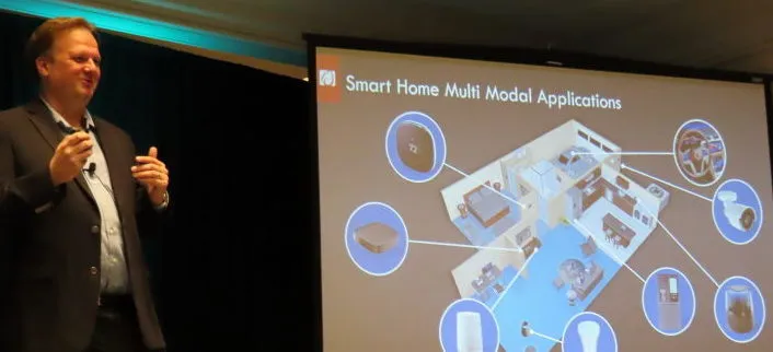
BoxThe last panel discussion, entitled Are the Tools in the Box? was moderated by the Consortium’s Jon Cheek. Participants included: VeriSilicon SVP David Jarmon; Arm PDG Marketing VP Kelvin Low; NXP’s Stefano Pietri, Technical Director of the company’s Microcontrollers Analog Design Team; Jamie Schaeffer, who’s GF’s Sr. Product Offering Manager for 22FDX and 12FDX; and Cadence Strategic Alliances Director Jonathan Smith. 2nd panel discussion, SOI Symposium, Silicon Valley 2019Yes, the tools are in the box. Smith of Cadence said they’re providing them, and NXP’s Pietro said that they’re very well positioned in his specialty, analog. VeriSilicon has IP, and anything they don’t have in house they’ll license. So why be afraid of body biasing? NXP has proof by example – they see such huge cost advantages that they try to leverage it as much as possible. GF’s doing training, since each area (automotive, IoT, etc.) has different needs. Some VeriSilicon customers already see such substantial benefits from FD-SOI that they’re not bothering to do biasing. Cadence points out that the Arm POP announcement is huge, and Arm’s Low wondered if the SOI Consortium could do an IP portal? “Our sales departments need to explain the advantages to our customers!” said NXP’s Pietro.From the audience, NXP VP longtime FD-SOI proponent Ron Martino (who, btw, wrote some great articles for ASN when they first got into FD-SOI – read them here), asked why designers think FD-SOI means a lot of corners? How do we convince the industry that FD-SOI simplifies design? Cadence is working with GF, responded Smith, and will have some big new at Arm’s TechCon this fall. “We need more training and marketing to show it’s not scary," he added. For GF, the corners don’t get more complicated, and they’re working with Dolphin Integration on getting them covered early in the planning. Ease of access to IP will help, per Arm. And in a great concluding remark, VeriSilicon’s Jarmon said, “The craft is being automated. The more we work together, the greater success of FD-SOI.”
Read More
Today, the U.S. Trade Representative (USTR), as part of its Section 301 investigation into China's trade practices, released a list of approximately $300 billion worth of Chinese goods, including a number in the semiconductor supply chain, that would face a tariff of up to a 25 percent. SEMI is working with members to assess the industry impact and will submit written comments and testify against the tariffs at a public hearing scheduled for mid-June.SEMI encourages members to review the new list and determine the level, if any, of impact.Today’s announcement follows last Friday’s tariff hike from 10 percent to 25 percent on $200 billion of imports from China. All told, the U.S. already has levied tariffs on $250 billion of Chinese goods that include materials and machines critical to semiconductor manufacturing. The expanded list released Monday would impose tariffs on essentially all imports from China. For its part, China has announced retaliatory tariffs, but more are likely coming.SEMI has been steadfast in its opposition to these tariffs and other barriers to global commerce. Over the past year, SEMI has submitted numerous written comments and offered testimony on the damaging impact of tariffs to the semiconductor industry. While SEMI strongly supports efforts to strengthen intellectual property protections, we believe that the tariff increases will do nothing to address concerns over China’s trade practices but, instead, harm companies in the semiconductor supply chain by increasing business costs, introducing uncertainty and stifling innovation.SEMI will continue tracking ongoing trade developments. SEMI members with questions should contact Jay Chittooran, global public policy manager at SEMI, at [email protected].
Read More
Join us! In partnership with our members, the SOI Consortium is co-organizing and participating in two key SOI events coming up in China over the next few weeks. On May 18th, we’ve put together an SOI Forum at the World Semiconductor Congress (WCS) in Nanjing. And on May 23rd 24th, we’ve teamed up with our members SIMIT, Sitri and Leti for another in our series of SOI Academies, including an FD-SOI Training Day. (The last one this past winter was a terrific success – read about that here if you missed our coverage at the time.) QR code for WCS, Nanjing '19At WCS, the SOI Forum (sub-forum #8) is part of the afternoon Innovation Summit. We’ll cover the broader SOI ecosystem, including both RF-SOI and FD-SOI – from wafers to design through manufacturing. Presentations will be given by members of the SOI Consortium team, and by leaders from our membership, including Simgui, NXP, Incize, ST, IBM, Cadence and Xpeedic. Click here or scan the QR code for the full program and registration information. Also at WCS, SOI Consortium member VeriSilicon will be participating in a morning session on AI and IoT Wireless Communications (sub-forum #4). They’ll be giving a presentation on their low-power Bluetooth design platform for GlobalFoundries 22FDX, and their CEO Wayne Dai will be moderating a round-table discussion. You can get more information on that (in Chinese only, tho) here, or follow VeriSilicon on WeChat. QR code for SOI Academy and FD-SOI Training, Shanghaid 2019The SOI Academy in Shanghai is an opportunity for experienced designers to gain solid expertise in FD-SOI. The event begins in the afternoon of May 23rd with a series of informative plenary talks by members of the SOI Consortium team, and by experts from our members Leti, Soitec, VeriSilicon, GlobalFoundries and NXP. The FD-SOI Training starts the next morning, on May 24th.. This is a hands-on event lead by top experts from Leti. The morning is devoted to digital design in FD-SOI, and the afternoon to RF design (including for 5G) in FD-SOI. Attendees will get a comprehensive understanding of design techniques for low-power chips leveraging the multiple benefits and flexibility of FD-SOI technology. Get more information here, or from the WeChat QR code.We've got a busy schedule! To keep up to date with where we and our members will be promoting the SOI ecosystem, be sure to check our Events page regularly.
Read More
Why Is Smart Parking a Hot Topic? Poorly managed parking resources have a substantial negative impact on cities — one that has been well-documented. According to industry studies, poorly managed parking: Increases Traffic Congestion: 30% of traffic is caused by ongoing circling for parking. Increases Pollution: In Westwood, California, cruising for parking burned 47,000 gallons of gas and generated 730 tons of carbon dioxide in one year. Frustrates Drivers: Urban drivers spend an average of 20 minutes per trip looking for parking. Stifles Economic Opportunities: Traffic congestion cost Americans $124 billion in 2013, and this is predicted to rise to $186 billion by 2030. These problems are getting worse. As a result of growing urban populations, cities account for more than 80% of carbon emissions globally. Unplanned or inadequately managed urban expansion leads to rapid sprawl, pollution and environmental degradation. Due to the lack of parking-space availability, for example, Japan is ranked among the most expensive countries for paid parking. If left unaddressed, poor parking management will continue to plague cities, both large and small. Fortunately, Smart City Internet of Things (IoT) initiatives are helping cities to address their parking issues. IoT to the RescueThere are three key drivers of Smart City IoT initiatives. Cities want to: Improve the overall quality of life and mobility in urban environments Leverage technology to augment and improve existing infrastructure and services that citizens rely on every day Foster both economic and environmental improvements The availability of high-accuracy vehicle detection sensors coupled with affordable, low-power connectivity has enabled a new generation of Smart Parking technology. However, choosing the right Smart Parking solution is essential.High-accuracy vehicle detection sensors can provide valuable data to city planners and parking managers. This information includes: Parking availability Traffic flow Parking occupancy rate and historical data Turnover For parking management to effect change, city traffic managers, parking managers and urban planners need a holistic view of parking availability and usage patterns, and users need real-time information about available parking spaces.Sensors, cameras and communication networks form the basic infrastructure for Smart Parking. To deliver on the promise of IoT and to help cities improve the overall quality of life for residents and visitors, cities need a complete smart parking solution that provides: Accurate real-time vehicle detection and location of available parking spaces – significantly reduces the amount of time spent cruising for parking spaces, giving drivers the precise location of available spaces Connectivity from the sensor to the cloud – facilitates real-time parking data that city planners, parking enforcement and traffic managers can use to reduce traffic congestion Parking applications for cities, parking-lot owners and drivers — enables navigation to available parking and supports mobile payment, streamlining the parking process. Parking applications can also direct traffic enforcement personnel to parking violations as they occur, helping to alleviate traffic bottlenecks, such as double parking in loading zones. Such applications also improve the efficiency of other city services such as public transportation and garbage collection. Complete Smart Parking Solution – Sensor to Cloud (Source: PNI Sensor) To learn how cities are using Smart Parking sensors to improve the services they offer to residents and visitors, come see PNI at SEMI’s 2019 FLEX Japan MEMS Sensors Forum (May 22-23, Toyko, Japan). PNI President and CEO Becky Oh and PNI’s partner, Macnica Networks, will share Smart Parking use cases from innovative cities, corporate campuses and universities (Smart Parking presentation, May 22 from 16:55-17:25). Register for the conference today. For more information about PNI Sensor, visit the PNI Sensor website. Becky Oh is the president and CEO of PNI Sensor. Throughout her 20 years with the company, Ms. Oh has held a range of senior-level positions, from operations to technical business development. She received an M.S. degree in Electrical Engineering from Cornell University and a B.S. in Electrical Engineering and Computer Science from MIT. Ms. Oh holds multiple patents in the area of devices with multi-sensing and reporting capabilities.
Read More
SEMI is excited to recognize Elizabeth Lee of X-Fab as the SEMI Spotlight on Women Honoree for Q2 2019!Spotlight on SEMI Women celebrates the many accomplished women who work in the global microelectronics industry. Nominees in the quarterly spotlight include women who are beacons of knowledge, leaders of organizations and initiatives, hidden heroes and innovators in our industry. They are volunteers, protectors, intellectual disruptors and activists. Learn how you can nominate a woman for Spotlight on SEMI Women.Elizabeth Lee has loved technology from a young age. As a child, Elizabeth once took apart a broken VHS player and managed to repair the device, armed with nothing but a few simple tools and a strong sense of curiosity. After her more than 15 years in the microelectronics industry, it’s clear that this love – along with Elizabeth’s drive, curiosity, and tenacity – has allowed her to thrive in her career and have a significant impact as a leader not only as a quality systems engineer at X-Fab but in her community.Growing up in a rural Texas town of fewer than 200 people, Elizabeth found opportunities to learn about STEM extremely limited. Although Elizabeth’s interest in technology started at a young age, her first real learning opportunity came during a high-school computer science class. Fascinated by the physics of how computers work, Elizabeth became inspired to pursue electrical engineering at Texas Tech University after graduation.Elizabeth’s transition to university life was difficult. She struggled to balance life as a young mother with her studies and became frustrated when she saw no career path to electrical engineering. During her junior year at Texas Tech, Elizabeth was ready to move into a different field and requested a transfer into civil engineering. Looking back, Elizabeth sees this moment as a crucial turning point in her life that would eventually propel her into the semiconductor industry. Her academic advisor, also a woman, denied the transfer request and pushed Elizabeth to remain in electrical engineering. The advisor also urged Elizabeth to expand her focus outside of academics and get hands-on experience through undergraduate research.Elizabeth acted on the advice and found herself performing research at the Texas Tech nanotech center. She also began volunteering with West Texas BEST – a high-school robotics program that engages students in STEM and semiconductor technologies.Elizabeth has now volunteered for BEST for more than 18 years. She has served on its computer game development board, helping to design games and create rules, and contributed as an author. Elizabeth also served on the South Plains chapter of IEEE as secretary of the board, vice chair, chair, and is now an advisor for the TTU IEEE student brand of WiE (Women in Engineering).She is also a member of the Industrial Advisory Board of the Electrical and Computer Engineering department at Texas Tech University and the Faculty/Staff committee chair. More recently, Elizabeth participated in SEMI High Tech U (HTU), a STEM immersion program for high-school students, and will serve as an emcee for the third time in an upcoming HTU program. Elizabeth graduated with a master’s from Texas Tech after her research in MEMS biomedical lab-on-a-chip and quantum mechanics evaluation of AIO2 tunnel junctions. In 2004, she began her journey with X-Fab, where her responsibilities have included sustaining legacy node silicon technologies and developing yield improvement analysis techniques in the areas of silicon and silicon carbide. She was awarded the Technical Ladder distinction of Principal Engineer in 2015.Today, Elizabeth has more than 15 years of experience in quality, yield improvement, and process integration, all areas that support X-Fab foundry customers with yield and failure investigations. In addition to her technical accomplishments, she represented X-Fab as a Value Promoter, introducing new X-Fab employees to its core values. Over the course of Elizabeth’s career at X-Fab, she has continued to lead key improvement initiatives and dedicate herself to her community.Cristina Sandoval is manager of Workforce Development at SEMI.
Read More
Key takeaway #2: If you need a Goldilocks process node – where you'll get just the right balance between active power, unit cost and investment – look to FD-SOI. And, btw, the IP landscape has improved dramatically. Those were just some of the great points made by Huibert Verhoeven (shown above), GM/SVP of Synaptics' IoT Division in his talk at the recent SOI Symposium in Silicon Valley.BTW, if you missed part 1 of our coverage --Silicon Valley SOI Symposium a Huge Success. Key Takeaways (Part 1) Here. – you’ll want to be sure to read it, too. Almost all of the presentations are now posted on our website – click here to access them.In this post here, we’ll cover presentations by Synaptics, GlobalFoundries, STMicroelectronics, Anokiwave and Dolphin Integration. It was a really full, day, so be sure to stay turned for Part 3 of our coverage to follow shortly: it will highlight the remaining presentations and panel discussions.Synaptics: Smart Home at the EdgeSynaptics’ Verhoeven’s presentation Revolutionizing User Experience Through Secure Neural Network Acceleration at the Edge was about Smart Home and using SOI. Synaptics is a human interface (HMI) company that’s been doing neural networks since 1986. They’ve always been on the leading edge, from their first shipment of PC touchpads to becoming a dominant force in all things HMI today: they now ship over a billion units annually. Synaptics slides 15 16 from the SOI Symposium, Silicon Valley 2019.They currently have SOI products shipping with dedicated neural networks for voice, he said. European [privacy] regulations have played a part in driving their use of SOI, as have challenges regarding power and heat. Things are getting smarter at the edge. For example, not only do users want their coffee machine to offer the usual morning espresso, Synaptics says that the next step is for your coffee machine to recognize you’re looking extra tired and ask if you might want a double?! For them Smart Home and multi-modal applications are the primary area of interest, as well as some automotive. Although their biggest customers have resources, others need guidance. Voice is a critical component, but now you also need video and display.Why SOI? Their HMI vision requires low power, significant computation and dedicated neural network hardware, explained Verhoeven, so FD-SOI with RF meets their needs. “22nm SOI is a Goldilocks IoT Process Node,” he proclaimed. It gets the combination of active power, unit cost and investment just right. What’s more, he said, “The IP landscape has improved dramatically. Our choice of SOI was not an accident.” Be on the lookout for more products leveraging FD-SOI over the next six months, he concluded. At this point on SOI, they’ve got 1 TOPS products with dedicated NPU for speakers, soundbars, Wi-Fi mesh, appliances, STBs and smart displays. These products have voice and sensor real-time (RT) AI. Next up is 4 TOPS on SOI with dedicated NPU, targeting STBs and smart displays with voice, video, imaging and RT AI. GF: World-Changing OppsGlobalFoundries slides 6 7 from the SOI Symposium 2019, Silicon Valley.“Our clients are at the forefront of changing the world,” declared Mark Granger, VP of the Automotive Product Line at GlobalFoundries. His presentation, Capturing High Growth Market Opportunities with SOI, detailed how mobility, automotive and IoT are the growth markets for SOI. So not unsurprisingly, GF’s 22nm FD-SOI technology, 22FDX, is seeing particular traction in mobile, edge, wearables and automotive. They’ve got twice as many tape-outs this year as they did a year ago, he noted. GF’s SOI portfolio includes 22FDX®, 45RFSOI and 8SW/7SW RF SOI for 5G/mobility; 22FDX for automotive (fully qualified for automotive Grade 2, with Grade 1 on the way); and 22FDX, 130RFSOI and 8SW/7SW RF SOI for IoT. GF has announced a stream of good news recently:with Dolphin Integration they’re delivering differentiated FD-SOI Adaptive Body Bias Solutions for 5G, IoT and automotive applications;they’ve crossed the billion-dollar design win threshold with 8SW RF SOI technology; they’ve collaborated with Synopsys to develop the industry’s first Automotive Grade 1 IP for their 22FDX process;and they worked with Rambus on the delivery of High-Speed SerDes on 22FDX® for communications and 5G applications.You might have heard about the Dolphin Integration news, as we covered it recently here at ASN (if not, be sure to read it here). Dolphin’s IP and methodology solutions address energy efficiency challenges. Automated transistor body biasing adjustment can achieve up to 7x energy efficiency with power supply as low as 0.4V on 22FDX designs. At the Silicon Valley event, Dolphin Integration CEO Philippe Berger provided additional information in his talk, FD-SOI IP Platform for Energy-Efficient IoT SoC. Dolphin Integration slides 5 6 from the SOI Symposium 2019, Silicon Valley.In another GF-related talk, Nitin Jain, the CTO of longtime GF RF-SOI customer Anokiwave presented Unleashing the mmWave Phase Array Using SOI for 5G Satcom. Anokiwave is a fabless semi IC company (you’ll find a good technical discussion of mmWave phase array written by their Chief Architect here). They do active antennas (aka phased array), something the military’s done for a long time, but now Anokiwave is bringing it to new markets and applications including radar, satcom and 5G. What they’ve been able to do is planarize the active antennas. They use GF’s 45RFSOI process technology for phased array systems because of the cost, performance, scalability and system enhancements it enables. 45RFSOI, he explained, is ideal for beam-forming FEMs (including the switches, LNAs and PAs). The move to 5G/mmWave is going to require a lot of antennas, so these Anokiwave ICs are headed to high volumes, concluded Jain.Stellar by STAs Roger Forchhammer, Director of Business Development at STMicroelectronics pointed out in his presentation, Automotive FD-SOI Microcontrollers with Embedded PCM, ST pioneered FD-SOI (and that was almost a decade ago, btw). Then in February 2019, they announced a world first: they’d begun sampling 28nm FD-SOI microcontrollers (MCUs) with embedded non-volatile memory (eNVM) based on embedded Phase-Change Memory (ePCM) to 10 alpha customers. These MCUs target powertrain systems, advanced and secure gateways, safety/ADAS applications, and vehicle electrification.STMicroelectronics slides 9 10 from the SOI Symposium 2019, Silicon Valley.(In case you want technical details, the breakthrough ePCM eNVM was first presented at IEDM in December 2018 – you can get the presentation that accompanied the paper, Truly Innovative 28nm FDSOI Technology for Automotive Microcontroller Applications embedding 16MB Phase Change Memory, from the ST website.)In his Silicon Valley presentation, Forchhammer said they’re now doing Stellar, a whole family of automotive products on FD-SOI. To do it, they’d taken an existing device and moved it to 28nm FD-SOI with ePCM, which they manufacture at their fab in Crolles, France. A major advantage for automotive he cites is that in software updates it’s bit-level programmable. “ST is fully behind FD-SOI,” he concluded, adding that we’re see more automotive as well as IoT products coming soon. Well folks, that’s all for this post. We’ll finish up our coverage of the SOI Consortium’s 2019 Silicon Valley Symposium in the next ASN post (there was so much to cover!). So please stay tuned.
Read More
Air pollution is one of the grand challenges facing the entire planet — from the wealthiest nations to the least developed. The World Health Organization reports that nine out of 10 people breathe air containing high levels of pollutants, and that polluted air takes over seven million lives annually through stroke, heart disease and respiratory ailments.As a result, the world is thirsty for reliable, high-performing chemical and environmental sensors that can provide previously unavailable real-time awareness of environmental conditions. On one level, this seems like a relatively simple step, given that smartphones are already equipped with miniaturized sensing technologies that can monitor our living environment and activities.While highly desirable, embedding air pollution sensors in common mobile and wearable devices has not been feasible previously because the necessary trade-offs between high performance and miniaturization have made it impossible.This situation drove a CEA-Leti team to develop a novel generation of fully integrated optical chemical sensors that leverage MEMS technologies. The team successfully merged multiple functionalities on the same chip, using integrated optics and photonics, fluidics, acoustics and electromechanical transduction. How did the team overcome significant technical obstacles to design a proof-of-concept device that senses multiple environmental pollutants — housed in a minimal hardware footprint?Advancing Chemical Sensor Capabilities with Silicon Featuring high selectivity, real-time performance, and fully reversible capabilities, optical chemical sensors are perfect candidates for industrial, environmental and biomedical applications. Consequently, in recent years, worldwide R D initiatives have invested substantial effort to improve them.R D programs have focused particularly on the mid-infrared (Mid-IR) wavelength range (2.5 - 12 µm) — also known as the molecule fingerprint region, which provides a unique combination of fundamental absorption order-of-magnitude bands and unambiguous identification of specific chemicals. A multitude of molecules generate strong and distinct absorption lines in the Mid-IR, providing a foundation for accurate spectroscopic detection. Traditionally, however, these sensors have required large and expensive lenses for infrared (IR) light, making them too big and costly for resource-constrained wearables and mobile devices.Fortunately, recent advances in integrated silicon photonics and quantum cascade laser (QCL) technologies have spurred investigation of new chemical sensor architectures. Richard Soref, a research professor at the University of Massachusetts Boston’s department of engineering, introduced the extension of Near-IR technology into the longer-wave Mid-IR infrared region in 2006. Soref’s concept showed that highly sensitive and selective gas sensors could be fabricated on planar substrates at low cost by co-integrating silicon MEMS, group IV photonics, and specifically designed III-V hetero-structures.While this approach showed promise, it preceded the widespread availability of most mobile devices and wearables. Foreseeing today’s proliferation of those devices, CEA-Leti developed the different building blocks required to implement these concepts in real devices.A New Concept of Integrated OpticsLeveraging these interesting findings, the institute developed a new combination of integrated optics and multiple sensor functions on a single chip: QCL sources, a photo-acoustic (PA) cell, and a mid-IR photonic integrated circuit (PIC) combiner. Their integration on a planar substrate (Figure 1) helped to achieve higher performance, new capabilities, and higher reliability at lower cost, all in a smaller package (less than a 1 cm3 or smaller than a 1-cent coin) with reduced weight and power consumption (less than 100 mJ per measurement). Figure 1: Fully integrated optical sensor (Courtesy: CEA Leti) This configuration represents a multi-gas-detection enabler. The PIC replaces costly, fragile discrete optics while the PA detector uses a MEMS microphone to replace bulky multi-pass cells.PA spectroscopy is among the most sensitive techniques available for monitoring chemical emissions or detecting gas traces. It relies on excitation of the chemical with a pulsed light source emitting at the absorption wavelengths of such molecules. The relaxation process creates local periodic variations of the temperature, resulting in stationary pressure waves, which high-performance microphones can detect.This new generation of devices, fully fabricated on silicon, shows performance comparable with state-of-the-art systems, with the huge bonus of small size and power efficiency that work well for mobile and wearable electronics. By supporting integration onto common technological platforms, such as on-chip photoacoustic sensors, researchers have successfully realized these miniaturized and cost-effective Mid-IR photonic devices in silicon. Mobile device and wearables manufacturers can now take advantage of manufacturable integrated devices for applications that are highly sensitive to size, performance and cost. Adding gas sensing to mobile devices and wearables is now very feasible.For more information on chemical sensing at CEA-Leti, please visit or contact: http://www.leti-cea.com/cea-tech/leti/englishCEA-Leti is an active member of SEMI-MEMS Sensors Industry Group. The technology research institute, along with Fraunhofer and imec, recently joined SEMI’s family as a Strategic Association Partner under a memorandum of understanding (MOU). Under this agreement, CEA-Leti will work with SEMI to advance technology roadmaps, industry standards and cutting-edge technologies including Internet of Things (IoT), artificial intelligence (AI) and machine learning that enable new capabilities across healthcare, automotive and other electronics manufacturing ecosystems. Sergio Nicoletti has more than 20 years of experience in micro and nanofabrication, including magnetic, superconducting and chemical sensing devices and technologies. Having joined CEA-Leti in 2006 as project manager for optical sensing devices used in chemical detection, Nicoletti is currently business development manager at the institute.Previous positions include research and project management at CNR-IMM (Bologna, Italy) and at Hitachi Global Storage Technologies. Nicoletti was also a visiting scientist at HGST (San Jose, Calif.), where he worked on magnetic recording-head devices.Nicoletti holds more than 20 patents and has more than 70 publications in peer-reviewed journals. In 2016, he was appointed coordinator of the European H2020 project MIRPHAB and is director of the project’s pilot line.Nicoletti received his Ph.D. in physics, with a focus on HTc superconducting devices, from Université Joseph Fourier (Grenoble, France). References“Photoacoustic cell on silicon for mid-infrared QCL-based spectroscopic analysis,” JG Coutard, A Glière, JM Fedeli, O Lartigue, J Skubich, G Aoust, A Teulle, T Strahl, S Nicoletti, M Carras, L Duraffourg. Proceedings Volume 10931, MOEMS and Miniaturized Systems XVIII; 109310V (2019) https://doi.org/10.1117/12.2506514“Miniaturization of mid-IR sensors on Si: challenges and perspectives,” S Nicoletti, JM Fédéli, M Fournier, P Labeye, P Barritault, A Marchant, A Glière, A Teulle, J Coutard, L Duraffourg - Silicon Proceedings Volume 10923, Silicon Photonics XIV; 109230H (2019) https://doi.org/10.1117/12.2506759
Read More
On the day I joined SEMI in March of 2017, I was filled with excitement to be on-boarding at a time when great, leaping strides in innovation were driving the rapid expansion of our ecosystem. In my many conversations with members that followed, I was not surprised that a vast majority ranked among their top concerns the persistent challenge of attracting, training and retaining the talent needed to grow their businesses. Later that year, I raised the global talent shortage issue in my article Securing Talent to Connect, Collaborate and Innovate. As an industry veteran I knew that the decades-long workforce development challenge will only worsen with the proliferation and increasing complexity of technology.Innovation has never been more technology-intensive. Developing the technology and producing the components required for applications powering next-generation communications (5G), artificial intelligence (AI) and machine learning, autonomous vehicles, and the Internet of Things (IoT) require bright minds in diverse fields of science to fill critical positions in the global electronics manufacturing industry. Today, that talent struggle is acute, threatening to undermine our industry’s potential to grow to $1 trillion by 2030.The electronics industry needs a comprehensive, integrated program to build the talent pipeline. The program should inspire school-age children to adult learners to pursue careers in this great but underrecognized industry. It needs to shine a spotlight on career opportunities. It must prepare workers with standardized skills sets transferable across the industry. And it must connect trained workers with hiring companies.SEMI is uniquely positioned to deliver this solution. Launched almost two years to the day after I joined SEMI, SEMI Works is SEMI’s branded workforce development initiative. We realize that trade associations don’t create jobs. Their members do. Think of SEMI Works as SEMI’s commitment to build and maintain the needed infrastructure – the talent pipeline. SEMI Works is comprehensive. The program, supported by SEMI members, is a wide-ranging effort by our Global Advocacy team to ensure education is demand-driven, training programs better meet the needs of the industry, more people pursue careers in electronics and our members have access to the talent pool that we are cultivating. With SEMI Works, SEMI is developing scalable solutions to improve connections among training and education providers, prospective workers and the industry. Key features of SEMI Works will include SEMI-certified education courses and training programs linked to industry requirements and skills credentialing for workers.SEMI Works starts with raising awareness of SEMI-certified programs as a key bridge connecting prospective talent, the industry and applicable training and education programs. Growing awareness of the programs will enable SEMI to build an extensive database of employers and qualified talent and link both to the right training. SEMI will continue to drive and endorse programs that help meet member needs throughout the education continuum – from K-4 to higher education and adult training. But the infrastructure and ecosystem required to support and scale these programs is the key for all of us to win together. At a high level, SEMI Works consists of several important components: Linking the required industry competencies to education and training course curriculum – Similar to the establishment of SEMI standards, SEMI will certify education and training programs that dovetail with the industry competency model. Initial certification and annual re-certification ensure continued updates, relevance and sustainability of the programs. SEMI will raise awareness of SEMI Works certified programs as the standard for meeting the industry’s talent requirements. Developing and maintaining the electronics industry competency model – Through established working groups and ongoing dialogue with our members, we are developing a competency model – a tiered matrix of required competencies used to link course curriculum to the talent needs of employers. The competency model consists of interpersonal and individual skills, academic and general industry requirements, advanced manufacturing competencies, and competencies by job. SEMI will establish and maintain the model with regular updates. Improving access to talent – Through SEMI Works, SEMI will build an extensive database that brings together programs, talent and employers. People and organizations opting into a SEMI-certified program or acquiring a SEMI program certification will be part of the SEMI database. Job seekers will be able to set up a profile and resume and search for training and employment opportunities, and employers will search the talent pool – much as job-search sites work today – assured of a skills match based on the SEMI certification. I am passionate about education and proud of all of SEMI’s efforts. I am especially proud of the work we are doing to help provide a pathway to meaningful careers for children and adults all around the world. We no longer have the luxury of a piecemeal approach to training and education.It is my hope and belief that SEMI Works, together with our efforts to improve diversity and inclusion in the workforce, will be SEMI’s lasting mark on the global electronics industry.Ajit Manocha is president and CEO of SEMI.
Read More