downloadGroupGroupnoun_press release_995423_000000 copyGroupnoun_Feed_96767_000000Group 19noun_pictures_1817522_000000Member company iconResource item iconStore item iconGroup 19Group 19noun_Photo_2085192_000000 Copynoun_presentation_2096081_000000Group 19Group Copy 7noun_webinar_692730_000000Path
Skip to main content
Smart car technology is on the fast track. According to a forecast by the Consumer Technology Association, revenue for North American technology will reach $398 billion in 2019, with sales of emerging technologies related to automotive electronics alone expected to hit $17 billion, a 9 percent increase over 2018. Growth of automotive electronics in the semiconductor application market is on pace to exceed 10 percent for the first time, with a 11.9 percent annual compound growth rate from 2017 to 2022, said Peng Maorong, research manager of ITRI Industrial International. Today, automotive electronics trails only personal computers and mobile devices in driving semiconductor market revenue. For its part, Automotive World 2019, the world's largest exhibition for advanced automotive technologies, has drawn even more attention in recent years. The event consists of six exhibitions, including automotive electronics technology, auto parts, drive systems, lightweight materials, autopilot technology and car networking, and featured demonstrations of compelling technologies including an AI deep learning module (Xilinx) and high-speed car intranet technology (Israeli manufacturer Valens). Toyota is also on the cutting edge of automotive electronics with the rapid maturity of its semiconductors, AI technology and materials, and complete network technology. The carmaker is no longer just a pure-play automotive manufacturer. Instead, the automotive giant is positioning itself as a car service provider (mobility service provider) and plans to team with ride-sharing providers such as UBER and Didi and other automotive technology providers in the future.Taiwan, with its strong semiconductor industry chain and a complete ecosystem of information communication, will be a key force in the automotive market as the region looks to cross-industry and cross-border cooperation to help power the market. To help the automotive electronics industry seize the market promise of smart cars, SEMI established the Global Automotive Electronics Advisory Committee (GAAC), with members including Audi, Bosch, Denso, Ford, Honda, Nissan, Volkswagen, Amkor, Infineon, NXP, Synopsys and Wanghong. More than 30 international companies, spanning Europe, the United States, Japan and other regions are represented on the committee. The committee met for the first time this month in Taiwan to help leverage the prowess of Taiwan's microelectronics supply chain in advancing international automotive electronics, better link Taiwan to international trends, and give Taiwan a bigger voice in the emerging smart car market, and create more opportunities for resource integration across borders. To learn more about GAAC, contact Helen Chen Chen Huiyu | Email: [email protected] | Phone: (03) 560-1777 #112.Extended reading: smart car Baihua Qi will be the next wave of killer applications (on)Emmy Yi is a marketing specialist at SEMI Taiwan.
Read More
Have you ever wondered if you could “feel” what it’s like to revisit your favorite vacation spot while sitting on a couch in your living room? How about walk through a restaurant overlooking the water’s edge as you enjoy a savory dish, while still sitting on that couch?If you follow trends in consumer electronics, you probably imagined a virtual reality (VR) headset that uses a visual interface to simulate the ambiance of the restaurant as you use a voice interface to scroll through the restaurant’s menu. While the tech world has made great progress in evolving the visual and voice interfaces of VR, immersive virtual food-tasting also requires a digital interface that supports a sense of smell and taste. In fact, the National University of Singapore is conducting research on the topic (see the video), and Project Nourished claims to enable “eating and drinking in a whole new way – by hacking vision, gustation, olfaction, audition and touch – with or without caloric intake” – through VR.We’ve already come a long way in our quest to replicate human senses such as touch, vision (via biometric authentication) and voice to build user interfaces to interact with the digital devices around us. In fact, every invention that permanently changed the consumer electronics landscape in the last few decades has in turn brought to life one of these user interfaces (UI). For example, smartphones proliferated touch, video games such as Nintendo Wii and Sony Xbox brought gesture, and most recently, smart speakers and VR headsets have increased the adaptation of voice and vision.Complexities of UI DesignUI design is a complicated task that builds upon years of research in neuroscience, cognitive thinking and engineering. It must also account for individuality because users interact differently with their digital devices. Some, like me, use their left hand predominantly when interacting with a gaming console. Some have a heavy accent, which can make speech recognition difficult, while those with a hearing disability may prefer touch over voice as a user interface. Application, context and proximity of the device to the user also affect UI. For example, a user interacting with a smartphone at home has the option to touch or speak to the device whereas voice is the safest means to communicate with a car’s infotainment system while driving.Consumers often bring their digital devices wherever they go, but still expect a consistent user experience. Therefore, a natural user experience is the key to UI adoption. A multi-sensory approach combining voice, vision and/or touch could prove the most practical solution. For example, if I were to access my account at a bank ATM, I would prefer visual- or touch-interface authentication for security reasons, but I would still want to use a hands-free voice interaction to switch between the different menus on the machine. In this case, a combination of UIs could provide a more natural multi-sensory experience, albeit one that needs a careful design.UI technology development and adoption are largely influenced by the top four players in the consumer electronics industry – Apple, Amazon, Google and Samsung. Apple pioneered the touch interface with the invention of keyboard-less smartphones, and the rest of the industry followed suit. The introduction of Google Glass kickstarted the VR/augmented reality (AR) segment and opened new applications in the gaming and multimedia entertainment segments. While VR headsets work for gaming – and more recently for selling products and experiences – they are large and cumbersome devices that are uncomfortable to wear for extended periods. These are major hurdles for designers to solve. Voice, on the other hand, offers a hands-free user interface that is a more natural and frictionless compared to alternative UIs.A voice UI needs nothing but a voice command to interact with digital devices. However, it comes with its own complexity of varying user speech characteristics such as accent or volume. More importantly, the need to suppress various background noises for efficient use of voice UIs is critical. While edge computing and/or cloud-based artificial intelligence (AI) are critical technologies to enable battery life and performance of smart home devices, the overarching goal of conversational AI is still far from reality.From a business standpoint, the winner of the race for voice UIs must improve AI capabilities while supporting a strong ecosystem of partners. Amazon, for example, is king of this strategy. The e-commerce giant is building an Alexa Voice Service (AVS) ecosystem by way of its Alexa Fund companies and third-party integrations (partners) to realize its goal of proliferating voice everywhere. These partnerships enable the ecosystem to build end-to-end speech systems that can literally take voice interface products everywhere and promote, among other things, hardware startups that are disrupting the MEMS market with products such as environmentally robust piezoelectric microphones.Energy harvesting near-zero-power always-listening microphones, used in partnership with the AVS ecosystem, are enabling voice UI products to expand into battery-operated applications such as hands-free TV remotes, smart garbage cans, Bluetooth speakers, headsets, hardware appliances and automobiles. A good example of a unique voice UI launched at CES 2019: Housewares designer simplehuman’s voice-activated smart garbage can uses Vesper microphones and AVS. Watch the video.While the future might bring additional digital interfaces, along with multisensory experiences using vision, gesture and touch, voice UI is at the forefront of current technological innovation. Soon, Alexa might help cook dinner without intervention, even turning off the stove when food is burning through the use of a scent-detection sensor integrated with a microphone array. Voice UI continues to astound us with its possibilities, and we’re excited for the journey ahead.With more than 12 years of experience working in speech and voice applications for wireless devices, Udaynag Pisipati is a senior field applications engineer at Vesper. He holds a master’s degree in electrical engineering from University of Missouri and an MBA from Santa Clara University. A firm believer in speech as a natural user interface for human-machine interaction, Pisipati’s areas of interest include everything related to speech processing, including microphones/speakers, signal processing and machine learning.Vesper is a member of MEMS Sensors Industry Group (MSIG), SEMI technology community.
Read More
Editor's note: Arm and Samsung Foundry are extending their collaboration on FD-SOI, which they'll be highlighting at the SOI Consortium's Silicon Valley Symposium April 9th. In the meantime, Arm Senior Product Marketing Manager Umang Doshi described the range of projects in a recent Arm Community / Developer physical IP blog. We thank Arm for sharing this blog with ASN readers.~ ~~ Samsung Foundry and Arm FDSOI collaboration announced By Umang Doshi The challenge with designing at newer and more advanced process nodes is that things generally don’t get less complex and expensive, much as we might want this. Still, the upside to each new process node, generally, is that you can build more highly efficient and targeted devices to address more markets and applications in a timely fashion. For the complexity and cost challenges, however, there’s good news: Arm and Samsung Foundry just announced a comprehensive, foundry-sponsored physical IP platform, including an eMRAM compiler at 18FDS (18nm FDSOI). In addition, the Arm offerings for 18FDS include three POP IP packages for Arm Cortex-A55, Cortex-R52 and Cortex-M33 processor IP. The platform will help drive new leading-edge designs in power-sensitive applications in 5G, artificial intelligence (AI), automotive, Internet of Things (IoT), and other market segments. It’s the industry’s first, fully comprehensive physical IP platform that includes an eMRAM compiler at 18FDS. 28nm: Before the breakthrough One of the most widely embraced nodes, 28nm the so-called “forever node,” has done wonders for industry innovation over the years. However, leakage power is still challenging for planar transistors. Engineers deployed high-K metal gate (HKMG) at 28nm, to combat leakage, but it’s still an issue. That’s because the channel underneath the gate is too deep and too far from the gate to be well-controlled, which results in higher leakage power. Solutions for the leakage issue have prompted designers to embrace FinFETs and FDSOI (fully-depleted silicon-on-insulator) with thinner channels that enable greater control by the gate. Indeed, FDSOI is gaining traction in the market place. By construction, 28nm FDSOI enables much better transistor electrostatic characteristics versus conventional bulk technology. 28nm FDSOI offers: Wide Forward/Reverse Body-bias range and flexible Poly bias (PB) range to tradeoff power/performance. Better performance and power than bulk process technology. Better resistance to radiation and SER. Less sensitive to variability because there’s no channel doping. Ultra-low power voltage (operating at low voltages in the hundreds of millivolts range). Easy migration from bulk versus the previous SOI version, PDSOI (partially-depleted silicon-on-insulator), required unique timing and power models. What’s more, there are cost benefits today and more forecast for the future. Arm and Samsung Foundry extend FDSOI leadership from 28FDS to 18FDS In 2018, Arm announced the industry’s first Embedded MRAM (eMRAM) compiler IP built on Samsung Foundry’s 28FDS process technology. Since the announcement, Arm has engaged with several Samsung Advanced Foundry Ecosystem (SAFETM) partners on a landscape-changing collaboration to deliver the industry’s first 28FDS eMRAM-enabled IoT silicon system demonstrator telling the Arm IoT story on Samsung Foundry silicon. Coupled with Arm’s IoT ecosystem, Pelion IoT Platform and Platform Security Architecture (PSA) solutions, this 28FDS eMRAM-enabled IoT demonstrator will showcase a new-generation of secure and energy-efficient IoT edge devices which integrates software stacks offering secure boot, firmware updates, on-chip storage, chip to cloud communication and device/software provisioning. The combination of 28FDS and eMRAM non-volatile memory brings new opportunities for a new class of highly integrated and energy-efficient designs. We’re thrilled that Samsung Foundry has extended its successful collaboration on FDSOI technology from 28FDS process to 18FDS. With the new platform, 18FDS is a cost reduction solution with lower power and same back end of line (BEOL) as 14nm FinFET. It has RF and eMRAM support to enable the widest range of different applications. “18FDS is the next-generation node on Samsung's FD-SOI roadmap with enhanced power, performance, and area (PPA)," said Jaehong Park, executive vice president of Design Platform Development at Samsung Electronics. “The relationship between Samsung Foundry and Arm stretches back more than a decade and has helped put the right design technology in the hands of the world’s leading designers. The enhanced PPA from our 18FDS process combined with Arm cores and Artisan Physical IP will again bring the cost and time-to-market advantages to enable the competitive and differentiated SoC designs.” Highlights on Arm-Samsung 18FDS platform Includes seven memory compilers, three logic libraries, two (1.8 and 3.3V) GPIO libraries, three POP IPs and the eMRAM memory compiler. Supports automotive AEC-Q100 Grade 1 design requirements, and comes with ASIL-D support and a complete automotive safety package. Utilizes back biasing supported by the FDSOI technology to help achieve low leakage by using reverse body-bias technique or a performance boost using forward body-biasing. This is a key differentiation of 18FDS platform. Supports Logic Corner Generator (LCG) and Memory Compiler Corner Generator (MCCG). LCG and MCCG products allow designers to generate custom corners with body-bias voltages to take the maximum advantage of body biasing power-performance flexibility. 18FDS will help enable the development of new devices connecting consumers in entirely new ways, whether it’s in AI, 5G mobile, automotive or other areas. The platform will be available in late 2019. Arm's Physical Design Group has a track record of successful implementations with Samsung Foundry across multiple generations of process nodes and products. Besides 28/18FDS, Samsung Foundry and Arm also have 14LPP/LPC, 11LPP, 7LPP and 5LPE platform collaborations. Interested in knowing more about Artisan Physical IP at 28/18FDS? Come join us at SOI Silicon Valley Symposium on April 9 at Double Tree by Hilton, San Jose, California. During the event, you will have the opportunity to hear how Arm and other industry leaders work together to accelerate the adoption of FDSOI technologies including products and applications. Alternatively, you can also reach out to us with your inquiry.
Read More
Semiconductor, electronics and equipment manufacturers today face a number of logistics and supply chain challenges that could be overcome by systems providing a secure, tamper-resistant, single source of truth. Chief among these challenges is limited data sharing due to data security barriers among suppliers, shippers, manufacturers and test houses, an impediment to achieving optimal product quality and regulatory compliance. Additionally, inefficient and inadequate processes for tracking goods make it more difficult to isolate shipping problems, track faulty parts and verify product authenticity. Counterfeiting has become a serious problem that costs US-based semiconductor manufacturers $7.5 billion annually.How Blockchain Can Help Clear Data Sharing BottlenecksBlockchain functions could help alleviate many data sharing pain points in manufacturing. Blockchain’s distributed functionality, bundled security measures, and associated features such as smart contracts have the potential to help manufacturers quickly trace goods, manage records transparently, and automate supply chain processes and payments. No isolated blockchain platform would solve all of these problems on its own. But, when combined with other solutions and applied to particular use cases, blockchain has the potential to optimize operations and foster an environment of trust and collaboration among consortium members. Three core features of blockchain make it a valuable technology for manufacturing: Distributed and immutable system of record. With a distributed system of record in the blockchain network, there is no "central" data store controlled by one organization. The distributed ledger provides all participants with a view into the data, thus increasing transparency, data distribution timeliness, information sharing, and data access. Security also improves as there is no single central data store open to external attacks. Once data is inserted onto the chain, it cannot be easily changed. Security and Trust. Blockchain integrates best-of-breed cryptographic mechanisms to guarantee the digital identity of the network participants and secure the privacy of the data stored to enable role-based data access. It brings trust to a potentially trustless environment without the need for a centralized third party. Smart Contracts. Smart contracts are embedded business logic that can be added to a blockchain. They enable the automation of many processes and the secure handling of contracts. Blockchain Use Cases in ManufacturingIn each stage of manufacturing, blockchain could be applied in a variety of use cases to expedite processes and alleviate security issues. A few examples that merely scratch the surface of what may be possible follow.In pre-production, manufacturers may implement blockchain solutions for Collaborative Planning, Forecasting and Replenishment (CPFR). These systems monitor inventory levels, enabling suppliers to replenish supplies before they run low. The expensive, proprietary B2B networks used today could be replaced with blockchain as the common sharing protocol, using non-proprietary or public networks.Suppliers may also combine blockchain with IoT sensors on shipping containers to provide a tamper-resistant record of shipping conditions. This could be used to ensure that temperature and humidity tolerances for chemicals and equipment are not exceeded during transit from the supplier. The identity and materials in components and subcomponents of manufacturing equipment could be collected on a blockchain to verify compliance with environmental and health regulations. During production, a manufacturing process machine can be registered on a blockchain with a unique identity; its performance and maintenance history can be recorded. A maintenance service provider could then be automatically notified, via a smart contract, when a predictive maintenance alert is written, allowing repair of machines before they fail. In the distribution stage, customers could search the ledger for a product’s complete history, reducing counterfeiting and solidifying the origin of properly sourced goods. When faulty product is identified, the manufacturer may search the ledger to quickly locate the faulty supplier or bad test results and alert all receivers of the defective product.ConclusionWith blockchain, manufacturing can become a more collaborative process among suppliers, manufacturers and customers. Blockchain can help streamline the supply chain and inventory replenishment, improve tracking and regulatory compliance, and reduce counterfeiting. Augmenting blockchain with IoT enables use cases like predictive maintenance and monitoring of goods during transit. Blockchain is not yet mature and its business value still needs to be proven. However, it is poised to help manufacturers decrease costs and fraud, and provide customers with faster, more secure delivery, increased visibility, and consistency.More Resources on Blockchain and ManufacturingTibco is an active member of SEMI’s Smart Manufacturing Technology Community, which holds regular meetings on this and other topics. Join now to help shape the future of Smart Manufacturing. For more information on blockchain use cases in manufacturing, please see these resources. Read this Whitepaper: Blockchain and Manufacturing: A Match Made in the Factory Watch this Webinar: Blockchain and Manufacturing - A Match Made in the Factory Visit the TIBCO Blockchain Solutions page Mike Alperin is a TIBCO principal manufacturing industry consultant embedded in the Data Science team where he applies analytics, machine learning and big data technology to current industry problems. Prior to this he was the product manager for a leading commercial yield management application. He has worked at start-ups and global semiconductor manufacturing companies as a yield manager, device engineer, process engineer and failure analyst. Mike is based in Austin, Texas.
Read More
FD-SOI for RF and mmWave communications is a hot topic. In high-data rate communications like RF and millimeter-wave devices in particular, FD-SOI delivers high-performance with numerous unique advantages, making it most likely the fastest RF-CMOS technology on the market. If you’d like to take a deep dive and learn more about it, Soitec and Incize are sponsoring a free, full-day workshop in Grenoble on April 4th, 2019. Click here for registration information. The workshop follows the day after the IEEE/EDS EuroSOI-ULIS conference there (you can read about the full conference in a previous ASN post). This technical workshop will cover the FD-SOI technology platform with a focus on its compatibility with RF mmWave communications. Attendees will hear from notable FD-SOI leaders and experts from leading industry and research institutions presenting updates on key developments and building blocks across the semiconductor value chain. Topics will include circuit design, device fundamentals, simulation and characterization of RF devices, test, CMOS technology and substrate technologies enabling FD-SOI. In addition, the workshop will include an overview about how FD-SOI technology is benefiting current and future end user applications. Here’s the agenda: [caption id="attachment_15990" align="alignleft" width="945"] FD-SOI technology platform: new standards for emerging consumer electronics [Click to enlarge.][/caption]
Read More
I recently was part of a group brought together by SEMI to redefine SEMI E135, the standard applied to test methods for determining the transient response of a radio frequency (RF) generator used in RF power delivery systems for semiconductor processing equipment. Comprised of RF generator suppliers and end users, the team of approximately 15 people embarked on a two-year effort to modernize the standard.The key goals were: Rewrite the test standards so that design engineers can choose the right power source for a given application, for example atomic layer deposition, etching or other short-run processes. Ensure tests reflect real-world conditions. Create more transparency and communication between suppliers and users about the true capabilities of the power supply. The original standard is over 10 years old. It was defined prior to the widespread use of digital communication to control RF generators and limited to testing RF generators designed to deliver power to a nominal 50-Ω load. However, today’s semiconductor fabrication processes are dynamic, requiring RF generators to be able to ignite plasma and respond instantly to changing plasma conditions. Wafer quality and yield are highly dependent on power remaining stable even as plasma characteristics change and by the ability to quickly respond to a change in set point and other commands which result in power level changes.According to Paul Trio, Senior Manager, Strategic Initiatives at SEMI and Inna Skvortsova, of SEMI Standards, some device manufacturers have reported that more than half of RF generators used in semiconductor fabrication plants (fabs) fail within the first two years of operation. That is expensive for fabs in terms of downtime, unscheduled maintenance and total cost of ownership.SEMI E135-0918: Updated and Expanded Related Information SectionWith all of that in mind, we began a spirited, thorough collaboration resulting in a community effort aimed at advancing the industry. Discussions began within the SEMI SCIS Technology Community, a SEMI group focused on addressing component defectivity, and then complemented by the SEMI Standards program for formal standards development. During a series of meetings, we worked to update the standard so that it is easier to qualify a generator, provides guidance on data processing as well as setting up and performing tests. These improvements inevitably provide users better procedural details that will help them operate these generators in a safer manner. If you are at all familiar with SEMI E135 or other such standards documents, you know that what I just described is only a fraction of the information contained in the standard. Schematics, examples, illustrations are also included to help test engineers specify and report on the performance characteristics of an RF generator under test.The Related Information section of the newly revised SEMI E135 standard document is very important as it provides users additional helpful information on how best to use the prescribed test method. In it, the group chose to describe the limitations of testing equipment designed to deliver power to highly nonlinear loads using only linear loads.You’ll also find rationale for testing procedures, equations to determine gain, forward power and delivered power and guidance on test points. Again, what I’ve described here is only a brief sketch of what’s included; there is a great deal more information in this section that original equipment manufacturer (OEM) engineering teams, process engineers and technical teams evaluating RF generators should find useful.Healthy Competition for the Benefit of the Industry Now and in the FutureWe often talk about rapid changes in technology for our semiconductor customers, and how those advances help them meet their goals for improving yield and wafer quality or reducing total cost of ownership. Sometimes, technology development races ahead of standards, making it difficult for them to select an RF generator that best meets the performance demands the tool in their process will encounter.Advanced Energy and the semiconductor community have mutual, vested interests in helping customers make fully informed decisions, even though some stakeholders are competitors. Considering how fast the semiconductor market is evolving, with the advent to the IoT, 5G communications and Industrie 4.0, it’s critical that SEMI E135 and other standards reflect the state of the industry today and set the stage for the next-generation of RF power and control.This blog was republished with permission from Advanced Energy.
Read More
The 3D optical sensing market is once again surging – and it’s all thanks to Apple. What will we see in the next wave of end products enhanced by this technology, how will other market segments approach – and eventually use – 3D optical sensing, and which suppliers stand to gain the most from this very vital technology?Although 3D sensing, facial recognition and optical authentication systems have become only recently hot topics in the consumer electronics market, these mechanisms first made their appearance nearly a decade ago in November 2010. Following that debut, Microsoft soon launched the Kinect system in its Xbox 360 gaming console, marking a milestone as significant as Nintendo’s launch of its Nintendo Wii remote controller in 2010, which catapulted MEMS motion sensors into the high-volume consumer market.The Kinect system used a triangulation-based camera that Israeli developer PrimeSense Ltd. created and then licensed to Microsoft; Apple liked the technology so much that it acquired PrimeSense in 2013. The first version of Kinect applied the Structured Light (SL) method, a depth-sensing principle featuring an infrared (IR) laser projecting dots onto the scene, with a monochrome CMOS sensor measuring the differences in the acquired pattern. The second version of Kinect used the Time-of-Flight (ToF) principle.Kinect for Xbox360 was not only a successful consumer product; it also sparked a new market, thanks to the relatively low cost of the 3D sensing solution. By using the same hardware for Xbox 360 as in its first version of Kinect, Microsoft allowed developers to design their pet projects in the Kinect environment. Adding hand gestures controls to a PC, creating a user-controlled virtual dynamic light (see Kimchi and Chips’ demo), and developing an inexpensive hologram generator (see “Princess Leia” video from the MIT Media Lab) are just a few examples of ecosystem developers and DIYers applying their creativity to Kinect.Apple Goes 3D with Face ID3D optical sensing has expanded from gaming consoles to the smartphone. In 2017 Apple presented its Face ID camera system for the iPhone X, which they launched to celebrate the 10-year anniversary of the iPhone. Face ID is the result of a longer term strategy for Apple, the byproduct of several company acquisitions to expand know-how in 3D sensing and augmented reality (AR)/virtual reality (VR). Between 2015 and 2018, Apple acquired the camera-module maker LinX (2015), the AR startup Vrvana and the imaging sensor firm InVisage Tech (both in 2017), and AR glasses’ designer Akonia Holographics (2018).For a company that has always innovated on its own terms, Apple’s idiosyncratic approach called for deployment of the Structured Light method combined with a ToF device. The result is an amalgamation that utilizes the best features of the two mechanisms, even if the combination is one that is expensive. Apple’s addition of a near-infrared illuminator to its ToF device enhances the system’s effectiveness under most light conditions while also improving the reliability of Face ID; the overall outcome is a more satisfying user experience. The ToF component, which STMicrolectronics supplies, makes use of so-called single-photon avalanche diode (SPAD) receivers that can work with any target material and color, although a higher target illumination is required to obtain good accuracy.The other core components of the Face ID system are the Vertical Cavity Surface Emitting Laser (VCSEL, from Lumentum) and a dot projector (from ams/Heptagon), assembled together in an optical package. Apple’s expensive but reliable approach explains the company’s inclusion of the Face ID system in its latest smartphone and tablet offerings – across the iPhone Xs, Xs Pro and Xr as well as in the latest iPad Pro models. Apple’s Face ID uses facial recognition for authentication on a range of iPhone and iPad Pro models. Image courtesy of Apple. Chinese Phone Makers Get into the GameMeanwhile, other mobile handset manufacturers are rumored to be working on Face ID-like systems or have already presented similar solutions, albeit through a variety of approaches. Some have chosen to use standard ToF devices while others have adopted an SL tactic. In many of these designs, which happen to target Android systems, OEMs generally include a fingerprint sensor as a fallback biometric option to their own nascent 3D facial recognition systems. The fingerprint sensor operates in either standalone mode or integrates into the display.Chinese handset maker Oppo, for instance, uses the SL method on its Find X model with algorithms coming from Megvii. Oppo claims its equivalent of Apple Face ID is faster. I have heard that Vivo has been working on a ToF camera since mid-2018, which it claims provides greater accuracy and security in end-applications such as secure payments and unlocking the phone.Chinese technology giant Huawei’s first 3D facial sensor appeared in its Mate 20 Pro flagship mobile phone. Aside from providing facial biometrics, the front-facing 3D sensor doubles as a 3D scanner, enabling users to digitize live objects that they can then manipulate in 3D AR applications. While still a novelty, the application highlights the use of 3D light sensors beyond that of biometrics. Xiaomi’s Mi Explorer Edition smartphone features a complex SL 3D module to enable 3D facial scanning although it looks like a clone of the Apple solution.Overall, the importance of facial recognition is no longer a matter of dispute, given that Apple’s rivals are now developing counterpart offerings of their own. Leaked code from the next revision of the Android operating system (revision Q), now under development by Google, has confirmed as much. Big and Getting BiggerIHS Markit forecasts that global revenue for ToF sensors in the 3D optical sensing market will surpass $500 million in 2019, up from $370 million last year. We also predict that the ToF market will grow in the coming years, spurred by combo solutions integrated with other light sensors in the same package. This will lead to a cheaper bill of materials (BOM) compared to the BOM for the SL method.At the same time, IHS Markit forecasts that the total market potential for light sensors will be worth much more, reaching $1.5 billion by year 2022. That’s because after a solid start with gaming consoles, 3D sensing has matured and consolidated in the massive smartphone arena.A segment of 3D Sensing’s future growth will come from other use cases and applications that are emerging outside consumer electronics and mobile. These include people-counting and -tracking in consumer and industrial applications, landing-aid and obstacle-avoidance functions in drones, and car-trunk (boot) opening with foot gestures, as well as gesture recognition and passenger detection in automotive. IHS Markit predicts steady growth for ToF and other light sensors. All told, the ToF approach appears to have a greater chance than the SL method in gaining a larger market share, leading to a cheaper and smaller BOM along with reduced integration costs in system assembly and calibration.Sometime this year, Apple and other handset OEMs may include a ToF-based 3D camera on the back of the iPhone to support more immersive gaming experiences and new AR/VR applications. This will further boost the 3D sensing market.To be sure, other mature technologies are available as valid alternatives to optical 3D sensing, including ultrasonic, mmWave and radar. These alternative technologies may gain part of the total market now commanded by 3D sensing, in use cases such as obstacle-avoidance or in-cabin presence detection.To learn about 3D Optical Sensing and Light Sensors from IHS Markit, go to: https://technology.ihs.com/606483/light-sensors-for-consumer-mobile-report-2018Manuel Tagliavini, a principal research analyst at IHS Markit, covers MEMS and sensors technology.Manuel Tagliavini joined IHS Markit in 2017. His key areas of focus are MEMS and sensors for mobile and consumer technologies. He is responsible for the tracking of sensors in handsets, tablets, laptops, and sports and fitness products.Prior to IHS Markit, he spent over 10 years with STMicroelectronics, working in various roles including product engineering, program management, and marketing and business development in the company's MEMS division.Tagliavini earned an Executive Master of Business Administration at SDA Bocconi School of Management and a Master of Science in Electronic Engineering from the University of Parma, both in Italy.Stay tuned with the technological advances and market trends in the MEMS Sensors ecosystem. Join MEMS Sensors Industry Group (MSIG), the SEMI technology community that connects the MEMS and sensors supply network in established and emerging markets, allowing members to grow and prosper.
Read More
[caption id="attachment_15930" align="alignright" width="150"] Daniel Nenni, CEO Founder, SemiWiki.com[/caption] Note to our readers: Semiwiki Founder Dan Nenni recently wrote an excellent piece on the importance of the Synopsys investment in automotive IP for GlobalFoundries' 22FDX (FD-SOI) technology. He graciously has given us permission to reprint it here in ASN. By Dan Nenni, CEO Founder, SemiWiki.com IP vendors have always had the inside track on the status of new process nodes and what customers are planning for their next designs. This is even more apparent now that systems companies are successfully doing their own chips by leveraging the massive amounts of commercial IP available today. Proving once again that IP really is the foundation of modern semiconductor design. Automotive is one of those market segments where systems companies are doing their own chips. We see this first hand on SemiWiki as we track automotive related blogs and the domains that read them. To date we have published 354 automotive blogs that have been viewed close to 1.5M times by more than 1k different domains. 
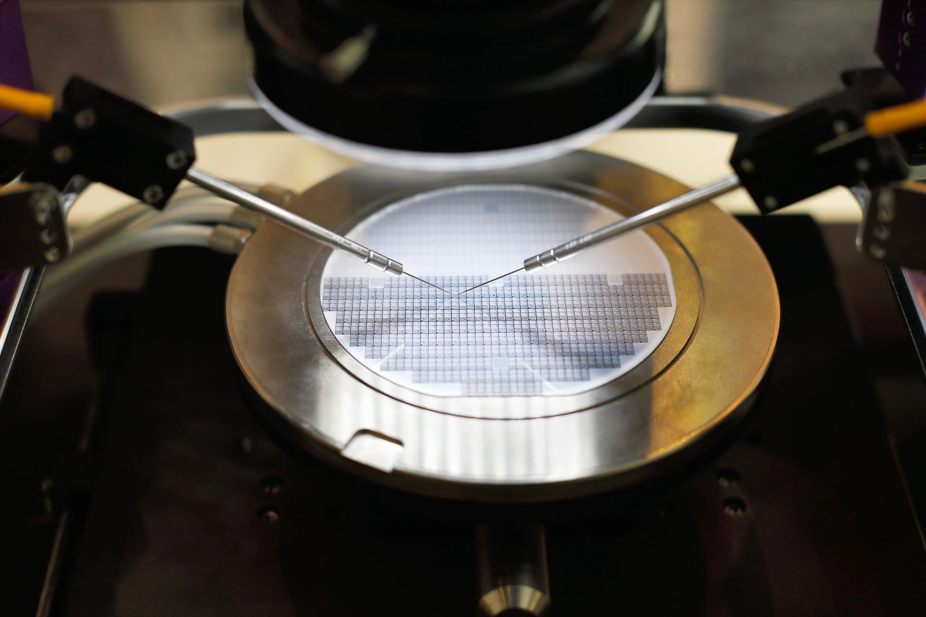
[caption id="attachment_15933" align="alignleft" width="1000"] (Courtesy: semiwiki.com and GlobalFoundries)[/caption] The recent press release by Synopsys and GLOBALFOUNDRIES didn’t get the coverage it deserved in my opinion and the coverage it got clearly missed the point. Synopsys, being the #1 EDA and #1 IP provider, has the semiconductor inside track like no other. For Synopsys to make such a big investment in FD-SOI (GF FDX) for automotive grade 1 IP is a huge testament to both the technology and the market segment, absolutely. I talked to John Koeter, Vice President of Marketing for IP, Services and System Level Solutions. John is a friend and one of the IP experts I trust. 3 years ago Synopsys got into automotive grade IP and racked up 25 different customer engagements just last year. The aftermarket electronics for adding intelligence (autonomous-like capabilities, cameras, lane and collision detection, etc...) to older vehicles is also heating up, especially in China. I also talked to Mark Granger, Vice President of Automotive Product Line Management at GLOBALFOUNDRIES. Mark has been at GF for two years, prior to that he was with NVIDIA working on autonomous chips with deep learning and artificial intelligence. According to Mark, GF's automotive experience started with the Singapore fabs acquired from Chartered in 2010. The next generation automotive chips will come from the Dresden FDX fabs which are right next door to the German automakers including my favorite, Porsche. One thing we talked about is the topology of the automotive silicon inside a car and the difference between central processing and edge chips. Remember, some of these chips will be on glass or mirrors or inside your powertrain. The edge chips are much more sensitive to power and cost so FDX is a great fit. Mark provided a GF link for more information: Here is the link to our Automotive resources: https://www.globalfoundries.com/mark...ons/automotive One thing Mark, John, and I agree on is that truly autonomous cars for the masses is still a ways out but we as an industry are working very hard to get there, absolutely. Here is the press release: Synopsys and GLOBALFOUNDRIES Collaborate to Develop Industry's First Automotive Grade 1 IP for 22FDX Process Synopsys' Portfolio of DesignWare Foundation, Analog, and Interface IP Accelerate ISO 26262 Qualification for ADAS, Powertrain, 5G, and Radar Automotive SoCs MOUNTAIN VIEW, Calif., and SANTA CLARA, Calif., Feb. 21, 2019 /PRNewswire/ -- Highlights: Synopsys DesignWare IP for automotive Grade 1 and Grade 2 temperature operation on GLOBALFOUNDRIES 22FDX®process includes Logic Libraries, Embedded Memories, Data Converters, LPDDR4, PCI Express 3.1, USB 2.0/3.1, and MIPI D-PHY IP Synopsys' IP solutions implement additional automotive-grade design rules for the 22FDX process to meet reliability and 15-year automotive operation requirements Synopsys' IP that supports AEC-Q100 temperature grades and ISO 26262 ASIL Readiness accelerates SoC reliability and functional safety assessments Join Synopsys and GLOBALFOUNDRIES at Mobile World Congress in Barcelona, Spain on Feb. 25 for a panel on "Intelligent Connectivity for a Data-Driven Future" Synopsys, Inc. (Nasdaq: SNPS) and GLOBALFOUNDRIES (GF) today announced a collaboration to develop a portfolio of automotive Grade 1 temperature (-40ºC to +150ºC junction) DesignWare® Foundation, Analog, and Interface IP for the GF 22-nanometer (nm) Fully-Depleted Silicon-On-Insulator (22FDX®) process. By providing IP that is designed for high-temperature operation on 22FDX, Synopsys enables designers to reduce their design effort and accelerate AEC-Q100 qualification of system-on-chips (SoCs) for automotive applications such as eMobility, 5G connectivity, advanced driver assistance systems (ADAS), and infotainment. The Synopsys DesignWare IP implements additional automotive design rules for the GF 22FDX process to meet stringent reliability and operation requirements. This latest collaboration complements Synopsys' broad portfolio of automotive-grade IP that provides ISO 26262 ASIL B Ready or ASIL D Ready certification, AEC-Q100 testing, and quality management. "Arbe's ultra-high-resolution radar is leveraging this cutting-edge technology that enabled us to create a unique radar solution and provide the missing link for autonomous vehicles and safe driver assistance," said Avi Bauer, vice president of R D at Arbe. "We need to work with leading companies who can support our technology innovation. GF's 22FDX technology, with Synopsys automotive-grade DesignWare IP, will help us meet automotive reliability and operation requirements and is critical to our success." "GF's close, collaborative relationships with leading automotive suppliers and ecosystem partners such as Synopsys have enabled advanced process technology solutions for a broad range of driving system applications," said Mark Ireland, vice president of ecosystem partnerships at GF. "The combination of our 22FDX process with Synopsys' DesignWare IP enables our mutual customers to speed the development and certification of their automotive SoCs, while meeting their performance, power, and area targets." "Synopsys' extensive investment in developing automotive-qualified IP for advanced processes, such as GF's 22FDX, helps designers accelerate their SoC-level qualifications for functional safety, reliability, and automotive quality," said John Koeter, vice president of marketing for IP at Synopsys. "Our close collaboration with GF mitigates risks for designers integrating DesignWare Foundation, Analog, and Interface IP into low-power, high-performance automotive SoCs on the 22FDX process." Resources For more information on Synopsys DesignWare IP for automotive Grade 1 temperature operation on GF's 22FDX process: Foundation IP: Logic Libraries, Embedded Memories, One-Time Programmable Non-Volatile Memories (OTP NVM), and Embedded Test and Repair Data Converters LPDDR4 PCI Express 3.1 USB 2.0/3.1 MIPI ~ ~ ~ About the Author Daniel Nenni has worked in Silicon Valley for over 35 years with computer manufacturers, electronic design automation software, and semiconductor intellectual property companies. He is the founder of SemiWiki.com (an open forum for semiconductor professionals) and the co-author and publisher of "Fabless: The Transformation of the Semiconductor Industry", "Mobile Unleashed: The Origin and Evolution of ARM Processors in our Devices" and "Prototypical: The Emergence of Prototyping for SoC Design". He is an internationally recognized business development professional for companies involved with the fabless semiconductor ecosystem.
Read More
MedTech, autonomous driving and other disruptive technologies will be in focus at the SEMI Industry Strategy Symposium (ISS Europe), 31 March - 2 April 2019 in Milan, Italy, as top European executives, researchers and academics gather to explore solutions to the region’s most pressing strategic, economic and social challenges. Ahead of ISS Europe, SEMI spoke with Mark Purdy, managing director and chief economist at Accenture Research, about Accenture’s Business Futures – four different future worlds set in 2025 based on the collision of trends across demographics, geopolitics, technology, and economics – and what these futures will mean for markets, workforces, operating models and industry value chains. SEMI: At ISS Europe in Milan, you will kick off the symposium highlighting market opportunities of the digital economy and how companies must adapt to competitive challenges. What inspired Accenture’s Business Futures four world scenarios?Purdy: The impetus for our Business Futures really stemmed from a certain dissatisfaction with current approaches to thinking about the future. We were struck by the following puzzle. First, there is no shortage of techniques for looking at the future, from forecasting to trends analysis to conventional scenarios. Second, most decision-makers have more or less the same access to information on global trends. Yet, time and again, we hear stories of businesses going bust or facing major challenges precisely because they failed to anticipate major changes in their industry.The paradox is that we have so much information, but so little real understanding of how the future actually unfolds. So that set us thinking about how to develop a new approach, based on a combination of detailed trend analysis, expert input and creative storytelling – which is what we call “Business Futures.” SEMI: Of demographics, geopolitics, technology, and economics, which trend do you see as particularly critical?Purdy: Actually, the essence of our Business Futures thinking is that it is the collision or combination of different trends – across economics, technology, demography, etc. – that shapes future outcomes, rather than individual trends per se. To a certain extent we tend to become fixated on specific trends and this can lead us astray or cause bad decision-making. For example, in the early 2000s many people saw very favorable trends in the U.S. economy – strong capital inflows, rapidly rising consumer spending, surging stock markets, and rising home ownership rates. Each trend in isolation looked strong and sustainable. But we failed to see how the combination of these trends was fueling risky financial innovation that would eventually lead to the financial crisis and great recession.Technology of course is a key trend. We are seeing tremendous advances in next-wave technologies such as robotics, machine learning, intelligent objects, 5G and virtualization. But we can only truly understand the impact of the technologies – and the business opportunities and challenges they create – by viewing them against a wider backdrop of changes in society, demography, geopolitics and economics. That is what Business Futures strives to do.SEMI: What will these different futures mean for markets, workforce, operating models and industry value chains?Purdy: There will be profound changes in how we think about all of these areas. Markets will become much more personalized and interactive. Technology will be increasingly integrated with humans, fueling innovation in areas such as personalized healthcare and preventative medicine. Our notions of distance and capacity will be upended, as new virtualized services enable new ways of reaching underserved customers. Consumers will become increasingly involved in the creation and design of products and services. New methods of innovation, powered by AI and virtualization, will come to the fore. New entrants will come from unexpected quarters, enabled by new technology. The upshot will be massive disruption and disintermediation of value chains across many sectors.SEMI: What can Europe do to prepare?Purdy: There are no simple answers, and the correct course will vary by country, but there are some basic things to get right. First, different countries need to understand their comparative advantage – for example, whether it is in services, new technologies, advanced manufacturing or resources – and work with the grain of these different futures. Second, countries need to ensure that they have the basic conditions – regulation, organizational adaptability, workforce flexibility, skills, and innovation infrastructure – to capitalize on the productive potential of new technologies such as AI, virtual reality, and the Internet of Things (IoT). Third, we need to create educational systems and workforce learning methods that emphasize creativity, problem solving and innovation – precisely the skills that will be most needed in an age of intelligent machines. SEMI: What are your expectations for the summit in Milan and for the future?Purdy: I’m very much looking forward to the ISS Europe Summit in Milan. As an economist, I believe we are at a pivotal moment in the semi-conductor industry, driven by waves of technological change and rising geopolitical frictions and uncertainty. With so many industry leaders and experts coming together at the Summit, I’m confident that our discussions will help point a way forward!Mark Purdy is managing director of economic research at Accenture Research. His research examines issues at the intersection of economics, technology and business. He has published widely in tier-1 media and specialised publications on topics such as China’s economy, emerging-market geographic strategy, inclusive economic growth, business futures and the economic impact of new technologies such as the Internet of Things and artificial intelligence. A graduate of Trinity College Dublin, he speaks on these topics at conferences and seminars around the world.Serena Brischetto is a marketing and communications manager at SEMI Europe.
Read More
For nearly two decades, Sean Ding, CTO and chief scientist of Alibaba Cloud IoT, has worked in software and algorithm architectures, sensing, semiconductors, systems and cloud computing – all areas that have contributed to the rise of the Internet of Things (IoT). It’s no surprise, then, that Alibaba is leading next-generation innovation for the IoT. Ding will bring his expertise to his role as moderator of Brave New World - MSIG Conference on AI+IoT 2019, a half-day forum March 20, 2019, at SEMICON China in Shanghai, China. Maria Vetrano of SEMI spoke with Ding about technologies key to the IoT era including MEMS, sensors, artificial intelligence (AI), edge gateways and cloud computing. SEMI: MEMS sensors are widely used in IoT devices. What is the relationship between AI and MEMS sensors?DING: While MEMS sensors and AI will increasingly co-reside in end-user devices, I do not recommend adding AI next to the sensor (in the same package). That’s because designers continue to use the ASIC for signal conditioning, so A/D converters are still required. Rather, we should look to edge gateways to carry the majority of the workload, including deep learning, because this reduces system complexity and power consumption.SEMI: Why are smarter sensors shifting data processing and analytics to the edge of IoT devices?DING: Data processing and analytics are very important for IoT devices, but we need to focus on understanding the data, parameter calibration and more. The MEMS sensor industry should leave big data analytics to edge computing and cloud computing because AI requires deep learning, demanding a huge amount of data.The challenge is to find the sweet spot for data processing right next to the sensor element.SEMI: What is China’s evolving role in innovation in MEMS sensors for IoT devices?DING: At present, the MEMS community in China needs to figure out how to innovate instead of copying existing technologies, a low-margin business that will not help to grow the industry. One reason why I am so pleased to see the MSIG Conference on AI+IoT in China is that it will encourage greater creativity in the MEMS community in China, and this will ultimately lead to Chinese companies and R D institutions leading innovation rather than copying it.SEMI: What is the right approach to combining smart MEMS sensors with AI in IoT devices? Why is this important for both domestic Chinese and international markets?DING: Combining data from sensors with cloud-edge computing is the right approach. As sensor companies increasingly provide end-to-end solutions, such as “sensor+ firmware + SaaS + app,” we will realize easier and faster integration of sensors in IoT applications.This is incredibly important because China today is the world’s biggest market for IoT hardware. China has 2,000-plus design houses, 200-plus OEMs and thousands of distributors. That said, we still see a highly fragmented market that will benefit from a faster integration methodology.Faster integration of MEMS sensors and AI/machine learning for IoT hardware will benefit designers in international markets as well.SEMI: What do you hope MISG Conference on AI+IoT attendees will take away from the forum? DING: MEMS sensors are highly fragmented, reflecting the highly fragmented applications in which they play. The MEMS sensors industry should figure out how to provide one-stop-shopping solutions for vertical markets. This will speed the scalability of applications and expedite the growth of sensor production. Sean Ding (柯镇) will moderate Brave New World - MSIG Conference on AI+IoT 2019 at SEMICON China on Wednesday, March 20, 2019, at Kerry Hotel Pudong in Shanghai, China.This conference has been organized by the MEMS Sensors Industry Group (MSIG). Register today to connect with Sean Ding and featured speakers at the event.Speakers at the MSIG Conference on AI+IoT 2019 at SEMICON China include: Welcome and Introduction / 欢迎辞Carmelo Sansone, Director, MEMS Sensors Industry Group (MSIG), a SEMI technology community AI Needs Accurate Data – MEMS Sensors Can Provide It / MEMS传感器为人工智能提供真实数据Andrea Onetti, Group VP of Analog MEMS Group, GM of MEMS Sensor Division, STMicroelectronics Enhanced IoT Edge by Smart Sensors / 智能传感器助力IoT边缘智Bennini Fouad, Regional President Asia Pacific, Bosch Sensortec Horizon AI Processor Solution, Enable Industries in AI Time / 地平线AI芯片解决方案,赋能千万业Carl Zhang 张永谦, General Manager/VP, Smart Chip Solutions Division, Horizon Robotics Inertial Sensors in AI Applications / 运动传感器AI应用案例Ben Lee 李彬 , CEO, mCube Ultra-Low-Power Solutions: an Ecosystem Approach / 超低功耗的生态链解决方案Carlos Mazure, IEEE Fellow, Chairman Executive Director, SOI Industry Consortium High-Integrity, Fault-Tolerant Open Inertial Measurement Platform for AI-based Vehicle Automation / 适用于人工智能车辆自动控制的高集成及容错的惯性测量开放平台Dan Dempsey, Senior Director of Automotive, ACEINNA Maria Vetrano is a public relations consultant at SEMI.
Read More