downloadGroupGroupnoun_press release_995423_000000 copyGroupnoun_Feed_96767_000000Group 19noun_pictures_1817522_000000Member company iconResource item iconStore item iconGroup 19Group 19noun_Photo_2085192_000000 Copynoun_presentation_2096081_000000Group 19Group Copy 7noun_webinar_692730_000000Path
Skip to main content
Default Banner Image

Singapore

Belgium France Germany Ireland Italy Japan Malaysia Singapore South Korea Taiwan United States Vietnam Image Business Training Featured Speakers

Leverage SEMI U learning offerings to wrap up your 2025 professional development journey! Our pledge remains unwavering: providing comprehensive, technical education to equip you with the skills needed for a prosperous journey in the semiconductor sector.

Are you ready to take your semiconductor industry knowledge to the next level? We're thrilled to invite you to our upcoming webinar titled "SEMI University - 2025 and beyond." This webinar promises to be an informative session where you'll gain insights into the latest updates, exciting live trainings at SEMICON West and virtually the remainder of this year and beyond. 

During this webinar, you can expect to:  

  • Discover the latest updates and enhancements to SEMI U's course catalog.  
  • Learn about the exciting live, in-person training courses scheduled for SEMICON West.
  • Review upcoming virtual instructor-led trainings.
  • Gain access to a special 10% discount on ALL on-demand courses.  


United States

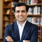
Headshot of Naresh Naik
Naresh Naik
Director, SEMI University
SEMI
SEMI U Workforce Development

Join us to discover our current course offerings, upcoming in-person and virtual trainings, and more. Engage in a Q&A session. Plus, by attending this free webinar, you'll receive a 10% discount code for all on-demand courses and will be entered into a raffle to win a FREE course bundle ($100 value). 

Choose your session:

8:00 am - 8:30 am Off Add to Calendar 2025-09-25 08:00:00 2025-09-25 08:30:00 SEMI University - 2025 & Beyond Join us to discover our current course offerings, upcoming in-person and virtual trainings, and more. Engage in a Q&A session. Plus, by attending this free webinar, you'll receive a 10% discount code for all on-demand courses and will be entered into a raffle to win a FREE course bundle ($100 value). Choose your session:US/EU: 8:00 AM – 8:30 AM PT [Register Now]Asia/US: 5:00 PM – 5:30 PM PT [Register Now] United States SEMI.org [email protected] America/Los_Angeles public Register Now
Event format
Promote in calendar
Off

SEMI Members:  $75

Use your corporate email address during log in to be recognized as a SEMI Member.

Non-Members:  $149

Students:  Free

Contact Andreia Smith-Moritz ([email protected]) with a picture of your student ID to receive your discount code.

Belgium Germany Singapore Taiwan United States FEMC 25 Recorded Tile Business Executive Technical
Highlighted content

Graphenea: Graphene Device Manufacturing

Graphene, a two-dimensional material with extraordinary electrical, mechanical, and biocompatible properties, is emerging as a key enabler for the next generation of medical devices. In this presentation, we will explore how Graphenea, through its advanced Graphene Foundry services, is driving the integration of graphene into scalable device manufacturing for biomedical applications. Attendees will gain insight into our end-to-end fabrication capabilities, from graphene synthesis, wafer-scale CVD graphene growth to cleanroom device prototyping and packaging. We will showcase examples of graphene-based biosensors, flexible electronics, and neural interfaces developed through our foundry platform, emphasizing their potential impact in diagnostics, monitoring, and therapeutic applications. The session will also address the challenges of material integration, process scalability, and regulatory pathways for graphene in medical technologies, providing a practical roadmap for researchers and companies looking to bring graphene-enabled devices from lab to market.

INBRAIN: Pioneering Precision Neuroelectronics: From Materials to Scalable Therapies

The convergence of materials science, artificial intelligence, and neuromodulation is transforming the future of neuroscience. This talk explores how high-density graphene-based brain-computer interfaces are enabling real-time decoding and precision modulation of neural circuits. Carolina Aguilar, CEO and Co-Founder of INBRAIN Neuroelectronics, will present the technological and clinical journey behind the world’s first graphene neural interface in humans, and how this platform is designed to deliver adaptive, patient-specific therapies for neurological disorders such as Parkinson’s disease. The session will highlight the translational path from research to regulated medical devices, and the role of Europe in leading responsible innovation in neurotechnology

ABOUT THE SPEAKERS:

Jesús de la Fuente

Jesús de la Fuente is the founder and CEO of Graphenea, a leading graphene production company established in 2010. Before founding Graphenea, he served as a Manager at Arthur Andersen, Director at PricewaterhouseCoopers in advisory professional services, and Managing Director at an industrial materials distribution company. He holds a Bachelor of Science in Engineering from Deusto University and an Executive MBA from IESE Business School. Under his leadership, Graphenea has become a world-leading graphene producer, contributing to the development of graphene applications across various sectors in over 60 countries.

Carolina Aguilar

Carolina Aguilar is the CEO and Co-Founder of INBRAIN Neuroelectronics, a neurotechnology company pioneering the use of graphene-based brain-computer interfaces for precision neuromodulation. With over 20 years of experience in healthcare, including 13 years at Medtronic where she led global businesses in brain modulation and diabetes, she has built a career at the intersection of innovation, neuroscience, and impact. Under her leadership, INBRAIN achieved the first-in-human implantation of a graphene neural interface and received FDA Breakthrough Device Designation. Carolina is also a 2025 World Economic Forum Technology Pioneer and a strong advocate for responsible, human-centric deep tech in Europe for the world.

United States

Jesús de la Fuente
Jesús de la Fuente
CEO
Graphenea
Carolina Aguilar
Carolina Aguilar
CEO and Co-Founder
INBRAIN
Gity Samadi
MODERATOR
Gity Samadi
Sr. Director, R&D Programs
SEMI
NBMC Smart MedTech FlexTech

Join us for this exciting Master Class with Jesús de la Fuente, Founder and CEO of Graphenea, and Carolina Aguilar, CEO and Co-Founder of INBRAIN, as they showcase their pioneering efforts of integrating graphene into scalable medical devices highlighting advancements in various medtech applications including biosensors and neural interfaces.

9:00 am - 11:00 am Off Add to Calendar 2025-09-10 09:00:00 2025-09-10 11:00:00 FEMC#25 Enabling Next-Generation Medical Devices: Graphene Device Manufacturing Join us for this exciting Master Class with Jesús de la Fuente, Founder and CEO of Graphenea, and Carolina Aguilar, CEO and Co-Founder of INBRAIN, as they showcase their pioneering efforts of integrating graphene into scalable medical devices highlighting advancements in various medtech applications including biosensors and neural interfaces. United States SEMI.org [email protected] America/Los_Angeles public Watch Now!
Event format
Promote in calendar
Off

Nijmegen, The Netherlands, 14 May 2025 — Trymax Semiconductor Equipment (Trymax), a leading provider of plasma- and UV-based solutions for semiconductor manufacturing, announces the installation of its 500th process chamber in Asia. This milestone reflects continued momentum across key regional markets—including China, Taiwan, South Korea, Malaysia, and the Philippines—and signals strong progress toward the company’s goal of 1,000 global installations by the end of 2025.

“Reaching 500 installations in Asia is a significant milestone for Trymax,” said Peter Dijkstra, Chief Commercial Officer at Trymax Semiconductor Equipment. “It reflects our team’s dedication to delivering practical, high-performance solutions with the speed and reliability that our customers need in order to stay competitive.”

Responsiveness as a Competitive Edge

In an industry where uptime, productivity, and reliability are critical, Trymax has earned a reputation for being highly responsive—from the inquiry stage to post-installation support. The company’s nimble structure allows it to take action quickly and decisively, enabling customers to manufacture with confidence. Many partners have cited the ease of communication with Trymax, and the timely support received, as reasons for early and continued engagement.

Supporting Asia’s Semiconductor Surge

Asia continues to lead global semiconductor growth, driven by accelerated adoption in high-demand sectors. Customers across the region are pushing forward with innovation and scale, particularly in:

• Automotive: The transition from internal combustion engine (ICE) vehicles to electric vehicles (EVs) is reshaping the industry. EVs require significantly more semiconductors—often up to 3,000 chips per vehicle—due to greater electrification, power management, and onboard computing systems. This shift is fueling demand for reliable, high-throughput semiconductor processing solutions.

• Artificial Intelligence (AI): The rise of AI and machine learning applications—from data centers to edge devices—is creating a surge in demand for advanced microprocessors and high-density memory. Backend processes play a critical role in ensuring the performance and yield of these complex chips, making equipment reliability and process control essential.

• 5G & Connectivity: Asia’s rapid deployment of 5G networks, combined with its mobile-first population and high-volume data consumption, is pushing the limits of semiconductor performance. This growth requires advanced packaging technologies, faster interconnects, and increased wafer-level precision—all of which depend on stable, repeatable backend processing steps.

Trymax’s plasma and UV curing technologies are designed to meet these demands, delivering proven results in ashing, descum, surface cleaning and activation, and isotropic etching. With a strong footprint across the region, the company continues to support customers at the forefront of innovation.

Forward Plans and Strategic Vision

To support its continued growth in Asia and globally, Trymax is advancing several strategic initiatives. The company is exploring plans to establish local manufacturing in China, a move aimed at strengthening supply chain resilience and improving responsiveness to regional customer needs.

As part of its 2025–2030 roadmap, Trymax is also deepening its collaborations with leading semiconductor manufacturers. By taking on selective, non-core process steps—particularly those related to backend wafer processing—Trymax helps larger players free up internal resources and maintain operational focus where it matters most.

In parallel, Trymax is expanding its role in advanced packaging. As integrated circuit (IC) designs evolve toward increasingly complex multi-layered stacks—sometimes comprising up to 16 layers—ensuring pristine, activated surfaces between each layer is critical. Trymax’s plasma solutions are engineered to meet these exacting standards, enabling customers to maintain high yield and reliability in next-generation device architectures.

Meet Trymax at SEMICON Southeast Asia 2025

Trymax will be showcasing its latest plasma-based innovations at SEMICON Southeast Asia 2025, from 20–22 May at the Sands Expo and Convention Centre, Marina Bay Sands, Singapore. Attendees are invited to meet the Trymax team at Booth #B1633 to learn more about the company’s technology roadmap and expansion plans.

###

About Trymax Semiconductor Equipment

Trymax’s core business is to support semiconductor manufacturers through the world with innovative plasma-based solutions for photoresist removal, surface cleaning, isotropic etch, as well as UV curing and charge erase applications, that are used in the fabrication of integrated circuits and other semiconductor devices. Trymax is a privately held company headquartered in Nijmegen, The Netherlands. Trymax operates regional sales and service offices in Europe, UA, China, Southeast Asia, Taiwan, and Japan.

Learn more at www.trymax-semiconductor.com.

Test Research, Inc. (TWSE: 3030), the leading test and inspection systems provider for the electronics manufacturing industry, is proud to announce its successful partnership with Bosch in the development of an AI visual check solution for MEMS packaging.

Bosch has recognized TRI's valuable contribution to their success in MEMS packaging in 2025 with a Certificate of Appreciation. The certificate acknowledges the successful completion of the AI visual check for MEMS packaging, highlighting the strong cooperation and partnership between the two companies.

This collaboration demonstrates TRI's expertise in AI-driven inspection solutions and its commitment to providing valuable solutions for the electronics manufacturing industry. TRI's AI-powered solutions include the AI Defect Detection, AI Smart Programming, AI Verify Host, AI training tool, AI Station, and more.

Please visit the following link to learn more about TRI's AI Solutions:
https://www.tri.com.tw/en/about/about-107-2-2.html

Learn more about the Bosch Group by following the link below:
https://www.bosch-presse.de/pressportal/de/en/company-page.html

###

About Test Research, Inc. (TRI)

TRI (TWSE: 3030), offers the most robust product portfolio in the industry for Automatic Test and Inspection solutions. Learn more at http://www.tri.com.tw. For sales and service information, please write to us at [email protected] or call +886-2-2832 8918.

Stanton Chase is pleased to announce that Sundar Rajan Ramalingam has joined the firm as a Partner in North America. His addition strengthens the firm's executive search and leadership consulting capabilities for the semiconductor sector at a time of rapid transformation.

Sundar brings nearly three decades of leadership experience across manufacturing and global technology sectors. He has scaled a multi-billion-dollar global engineering division and supported the growth of several Global Capability Centers (GCCs). Within the semiconductor ecosystem, he has played a pivotal role in building and advising leadership teams across chip design, chip-to-cloud platforms, semiconductor fabs, and foundry operations.

This deep operational and strategic background gives Sundar a unique perspective on the evolving talent needs of semiconductor organizations.

"The semiconductor industry is entering a pivotal era—what I call a 'perfect leadership storm'—driven by generative AI, strategic autonomy imperatives, and breakthroughs like 3nm and advanced packaging," said Sundar. "While these trends are accelerating innovation, the industry also faces a growing talent gap. Companies need capable leaders who can navigate complexity, scale innovation, and build resilient teams. I plan to use my experience in technology and manufacturing to help semiconductor companies find executives who deliver results and foster sustainable growth."

Sundar's career spans both strategic HR leadership and general management with P&L responsibility, offering clients a rare blend of technical insight and leadership development expertise.

"Sundar fits well with our North American team and fills a specific need in our practice," said Mickey Matthews, Managing Director at Stanton Chase in North America and Chair of the Governance Committee. "His time working across borders gives him a genuine understanding of how global teams function. Blending this multicultural understanding with Sundar's deep technology products and services vertical expertise matters a lot to the clients we serve and specifically in the semiconductor space."

Jan-Bart Smits, Managing Partner at Stanton Chase Amsterdam and Global Sector Leader for Semiconductors, added: "Sundar joins us when the semiconductor industry sits at a turning point. Firms in this sector are looking for something different in their executives—people who understand both market forces and engineering details. Sundar knows this world and will further enhance our ability to serve chip makers and their suppliers."

As the semiconductor industry moves into a new chapter—marked by AI-driven demand, geopolitical shifts, and the race toward next-gen nodes—Sundar's appointment signals Stanton Chase's commitment to helping clients lead with confidence and clarity.

Sundar holds an MBA from XLRI Jamshedpur (India) and completed executive education programs, including the Chief Human Resource Officer Program at Wharton, University of Pennsylvania.

He will serve clients from Stanton Chase offices in Baltimore and Raleigh, USA, as well as Bangalore, Hyderabad, and Chennai, India—locations near semiconductor business centers.

Click here to learn more about Sundar.

Click here to learn more about Stanton Chase's semiconductor expertise.

About Stanton Chase

Stanton Chase ranks among the top global retained executive search firms with more than 76 offices in 45 countries and a worldwide team of senior consultants. Stanton Chase serves clients across multiple industry specialties and places C-suite executives, senior managers, and board members for companies ranging from global corporations to emerging businesses. Stanton Chase belongs to the Association of Executive Search and Leadership Consultants (AESC), adhering to the highest industry standards of professionalism and ethics.

Belgium China France Germany India Ireland Italy Japan Malaysia Singapore South Korea Taiwan United States Vietnam Register Now Scope 3.11 800x800 Business Executive
Highlighted content

The webinar will address the following:

  1. Overall Contents of the Guidance
  2. Topics explored in creating the Guidance
  3. Intention of why the Guidance was developed
  4. Who was involved in the development
  5. Who should use the Guidance
  6. How it differs from existing standards and protocols

United States

Sustainability

Join the Leaders of the Semiconductor Climate Consortium Scope 3 Working Group, plus other industry experts, to review the recently released Scope 3 Category 11 GHG Assessment and Guidance for the Semiconductor Value Chain.  Compiled with the expert assistance of ERM, with input from all levels of the ecosystem, this document has been designed to align on reporting Scope 3, Category 11, an important step in measuring the impact of reduction efforts across the industry.

Download the Guidance Document

8:00 am - 9:00 am Off Add to Calendar 2025-06-12 08:00:00 2025-06-12 09:00:00 Webinar - Category 3.11 Review Join the Leaders of the Semiconductor Climate Consortium Scope 3 Working Group, plus other industry experts, to review the recently released Scope 3 Category 11 GHG Assessment and Guidance for the Semiconductor Value Chain.  Compiled with the expert assistance of ERM, with input from all levels of the ecosystem, this document has been designed to align on reporting Scope 3, Category 11, an important step in measuring the impact of reduction efforts across the industry.Download the Guidance Document United States SEMI.org [email protected] America/Los_Angeles public America/Los_Angeles
Event format
Promote in calendar
Off

Singapore, May 12, 2025 - DuPont (NYSE: DD) is excited to announce its participation in SEMICON Southeast Asia (SEMICON SEA), taking place May 20-22, 2025, in Singapore. At booth L3105, DuPont will showcase the latest offerings of Kalrez® perfluoroelastomer parts specifically designed for semiconductor and electronics applications, aimed at enhancing manufacturing efficiency and operational sustainability.

“Our new Kalrez® product offerings are engineered for enhanced sealing performance, significantly reducing leaks and pumping times,” said Dr. Meredith Dunbar, Kalrez® Global Technology Leader, DuPont. “In our continuous pursuit of sustainability, we have achieved improvements in sealing performance under harsh process conditions, which enable substantial waste reduction. These advancements make Kalrez® seals an ideal choice for the toughest challenges in semiconductor fabs, and also showcase our dedication to delivering high-quality, efficient, and environmentally responsible solutions.”

Highlighting this longstanding commitment to innovation, the Kalrez® brand is proud to celebrate its 50th anniversary this year. This milestone reflects five decades of excellence and dedication to developing high-performance sealing solutions tailored for critical applications in demanding environments. At this year’s SEMICON SEA exhibition, attendees will discover several key advancements, including:

Kalrez® Bonded Door Seal (BDS): Specifically designed for semiconductor manufacturing equipment, including applications like plasma etching, CVD, and PVD, Kalrez® BDS offers improved sealing performance over conventional O-rings by reducing particle generation, extending seal life, and minimizing maintenance downtime.

Bonding Methodology: An innovative bonding method developed by DuPont's technology team, allowing Kalrez® components to be fused with other functional materials, creating unique, composite-structured Kalrez® parts.

Custom Shaped Parts: Kalrez® custom perfluoroelastomer parts can be tailored to unique geometries for specific sealing applications and are available in various shapes and compounds to meet different thermal, chemical, and plasma resistance requirements. Custom parts can be produced as both volume production and prototypes.

DuPont is proud to be driving technological advancements in the Kalrez® product family and providing game-changing solutions to its customers worldwide. All SEMICON SEA attendees are invited to join in celebrating the 50th anniversary of Kalrez® and explore how Kalrez® products can support their innovation programs.

For more information about Kalrez® parts and applications, please visit www.kalrez.com.

About DuPont

DuPont (NYSE: DD) is a global innovation leader with technology-based materials and solutions that help transform industries and everyday life. Our employees apply diverse science and expertise to help customers advance their best ideas and deliver essential innovations in key markets, including electronics, transportation, construction, water, healthcare, and worker safety. More information about the company, its businesses, and solutions can be found at www.dupont.com. Investors can access information included on the Investor Relations section of the website at investors.dupont.com.

#   #   #

05/12/25

DuPont™, the DuPont Oval Logo, and all trademarks and service marks denoted with ™, ℠ or ® are owned by affiliates of DuPont de Nemours, Inc. unless otherwise noted. 

For further information, contact:

Rebekah Lazar
Semiconductor Technologies Communications Leader
DuPont
[email protected]

Cell: +1-302-509-1859

sigma design logo

Sigma Design Joins SEMI to Support Semiconductor and Electronics Industries

(April 1, 2025) - Camas, WA - Sigma Design, Inc., a leader in product development and engineering, is pleased to announce its membership in SEMI, the global industry association representing the semiconductor and electronics design and manufacturing supply chain.

By joining SEMI, Sigma Design gains access to an extensive network of industry leaders, market insights, and collaborative connections that enhance opportunities to deliver support services for semiconductor manufacturing, material handling and testing. This membership aligns with Sigma Design’s commitment to advancing technology and contributing to the growth of the semiconductor ecosystem.

Sigma Design is committed to driving innovation and excellence in support of the semiconductor industry. “Joining SEMI represents a significant step in that journey," said Yehudit Dagan, Director of Sales and Marketing at Sigma Design. “This membership will enable us to stay at the forefront of industry trends, enhance our support services for other SEMI members, and strengthen our ties with this community.”

As a SEMI member, Sigma Design looks forward to leveraging the organization’s resources to support the growth of the semiconductor ecosystem and reinforce its position as a trusted partner in the industry.

About Sigma Design

As product development experts, we are driven by new challenges. We design, engineer, build, and test solutions for our partners' success. Sigma Design is a full-service product development and engineering firm dedicated to solving complex challenges. With a focus on quality, efficiency, and innovation, Sigma Design provides end-to-end product development solutions that encompass design, engineering, manufacturing, testing, and staffing services. Committed to excellence, we exceed client expectations with our dedicated approach. Challenges Accepted. Solutions Delivered.


For more information, visit www.sigmadzn.com

About SEMI

SEMI® is the global industry association connecting over 3,000 member companies and 1.5 million professionals worldwide across the semiconductor and electronics design and manufacturing supply chain. We accelerate member collaboration on solutions to top industry challenges through Advocacy, Workforce Development, Sustainability, Supply Chain Management and other programs. Our SEMICON® expositions and events, technology communities, standards and market intelligence help advance our members’ business growth and innovations in design, devices, equipment, materials, services and software, enabling smarter, faster, more secure electronics. Visit www.semi.org, contact a regional office, and connect with SEMI on LinkedIn and X to learn more.  

[March 26, 2025 – Singapore] Test Research, Inc. (TRI), the leading test and inspection systems provider for the electronics manufacturing industry, will join SEMICON SEA held at the SANDS Expo and Convention Centre in Singapore from May 20 - 22, 2025. Visit booth #L2632 to learn about AI-powered AOI solutions for Advanced WLP/PLP and SEMI Back-End Package processes.

TRI will be exhibiting the new Wafer Inspection Platform, TR7950Q SII, featuring a High-resolution 2.5 μm 25MP camera and the TSV Metrology Module. The TR7950Q SII can perform Wafer Macroscopic 3D Inspection and micro measurement metrology. The TR7950Q SII can inspect Advanced WLP, Wafer Frame, Patterned Wafer, Wafer Bumping, WLCSP, through-silicon via (TSV), and more. The TR7950Q SII can measure TSV at ultra-high speeds, measuring sensing TSV depth, trench depth, oxide, nitride, PR, and PI film thickness.

Additionally, TRI will showcase the TR7007Q SII-S, the high-accuracy 3D SEMI SPI for precise solder measurements, supporting applications such as Mini-LED, C4 bumps (~100 μm Ø), and 008004 paste inspection. The lineup will also feature an X-ray Inspection Demo Station.

Join us at booth #L2632 at SEMICON SEA 2025 to discover TRI's cutting-edge SEMI inspection and metrology solutions!

Invitations and Registration

REGISTRATION FOR GCSW is CLOSED.  

All sessions are free of charge to Semiconductor Climate Consortium (SCC) and Energy Collaborative (EC) members.  Others will be admitted by invitation on a case-by-case basis.  Multiple attendees (up to 3) from your company are welcome, but must be invited. Exceptions can be made to the 3 persons limit to have the RIGHT people, with direct responsibility for subjects being discussed.

Belgium China France Germany Ireland Italy Japan Malaysia Singapore South Korea Taiwan United States Vietnam Interested in Attending? Business Executive Expositions
SEMI Logo Social Media
Logo_SQ_Google
scc logo
Highlighted content

Objective of GCS Workshops

A gathering of the semiconductor value chain in one place to most efficiently share solutions and tools and workshop solutions, thereby optimizing your time and resources dedicated to addressing the specific challenges we face. The GCS Workshops are co-hosted by SEMI, the Semiconductor Climate Consortium, Apple, and Google. 

The Workshops are focused on revealing the right details and data that will support action on decarbonization recommendations. The Workshops will NOT focus solely on the issue and roadblocks, but rather the solutions, including (1) sharing examples of successful paths, (2) provide possible tools you need to help address the gaps, and (3) active workshopping on further solution spacing towards emission reductions. We have identified leaders with the experience and knowledge to move toward answers during each Workshop. 

Bring your experience, critical thinking skills, and share with your fellow sustainability travelers.

Workshop Themes and Layout

5/15 – Opening + Facilities Abatement Tours (Tours are now full)

5/16 (AM) - Manufacturing Scope 1 Emissions – brownfield abatement retrofits, low GWP gas substitution and emission measurements reduction solutions, toolkits, roadblocks

5/16 (PM) - Manufacturing Energy Efficiency – fab/subfab interoperability, toolkits and ROI calculations

5/19 (AM) - Renewable Energy Education & Advocacy – global state-of-play, market breakouts for education and solution short listing

5/19 (PM) - Manufacturing Scope 3 Materials Decarbonization – partner paths, impacts and tools

5/20 (AM) - Data & Reporting Alignment – ROI and roadblocks + Closing (PM)

Synergies with the Semiconductor Climate Consortium 

Many themes of the GCS Workshops are outcomes of the discoveries in the SCC Working Groups and previous Supplier Day presentations.  The GCS Workshops will allow for greater depth of discussions and face-to-face solutioning opportunities.  With the right information and the right audience, attendees will depart with tools to operationalize for action.  Across the ecosystem, we want to see those benefits show up in our Scope 3 calculations. 

Microsoft Offices & Sands Convention Center
Singapore
Singapore

12:00 pm - 1:00 pm

Registration & Networking Lunch

Meet and connect with key industry stakeholders, policy leaders, and Microsoft’s sustainability leadership.

1:00 pm - 1:10 pm
Mousumi Bhat
Mousumi Bhat, PhD
VP SEMI Sustainability
SEMI

SEMI Global Climate Summit Workshops: Welcome

1:10 pm - 1:25 pm
Giorgio Fortunato
Giorgio Fortunato
Google

Energy in the APAC Region: Outlook & Strategies

1:30 pm - 1:45 am
susannah calvin
Susannah Calvin
Environment & Supply Chain Innovation
Apple, Inc.

Journey to Carbon Neutral - Supply Chain Focus

1:45 pm - 2:05 pm
Leslie Esparza
Leslie Esparza
Director, Responsible Sourcing
Microsoft
Leo Aspauza
Microsoft
William Hudson
Moderator
Will Hudson
Microsoft

Reflections on Microsoft Supplier Days & Looking Forward

2:05 pm - 2:15 pm
Mousumi Bhat
Mousumi Bhat, PhD
VP, Global Sustainability
SEMI

Overview of GCSW Workshops

2:15 pm - 6:30 pm

Facilities Abatement Tours

(Tours are full and no longer available to new registrants.)

Workshop 1: Manufacturing Fab Scope 1 Emissions

8:30 am - 8:50 am

Breakfast and Networking

8:50 am - 9:20 am
Beth Elroy
Beth Elroy
Vice President, Global EHS & Sustainability
Micron

Collaborative solutions for emissions challenges

9:20 am - 9:35 am
Cristal Phwan
Cristal Phwan
APAC Sustainability Team Manager
GlobalFoundries

Fabs Deploying new abatement tech; brownfield retrofits

9:35 am - 9:50 am
Robin Sim
Robin Sim
Facility Manager - Operation & Hookup Program
STMicroelectronics

Innovative ways to complete brownfield retrofits while minimizing fab disruption

9:50 am - 10:05 am
Hak Joon Kim
Dr. Hak Joon Kim
Principal Researcher
Korea Institute of Machinery and Materials (KIMM)

New abatement tech for both greenfield & brownfield fabs

10:05 am - 10:20 am
Haein Cho
Dr. Haein Cho
Samsung

Samsung's journey to net zero & Scope 1 strategies

10:20 am - 10:45 am

Workshop 1

- Retrofits: Learnings; forward-looking; benchmark projects; modular approaches
- Abatement Technology / Performance Roadmap: accelerating timelines; trends; alignment

10:45 am - 11:15 am
Scott Clendenning
Scott Clendenning, PhD
Intel
Gottfried Wastlbauer
Dr. Gottfried Wastlbauer
Head of Positioning & Business Model
Electronics business of Merck KGaA, Darmstadt, Germany

Low GWP Gases

11:15 am - 11:40 am

Workshop 2: Risk assessment & Methodology

11:40 am - 12:40 pm
Dr. Shou Nam Lee
Dr. Shou-Nan Li
ITRI
Rahul Singh
Dr. Rahul Singh
Manager, Emissions Analysis
Micron
Troy Boley
Troy Boley
President
Spectrum
Jonghan Lee
Jonghan Lee
SK Hynix

Emissions Measurement

12:40 pm - 1:05 pm

Workshop 3: Real-time monitoring, calibration variation, regulatory

1:05 pm - 1:30 pm

Readouts & Lunch Break

Workshop 2: Manufacturing Energy Efficiency – fab/subfab interoperability, toolkits and ROI calculations

1:30 pm - 2:00 pm
Kevin Chan
Kevin Chan
Lead, Artificial Intelligence
Micron

IDM perspective, state of the art sensor deployment & best practices for energy efficiency

2:00 pm - 2:15 pm
James Oh
James Oh
Aveva

Immediate Opportunities around Energy Efficiency

2:15 pm - 2:30 pm
John Golightly
John Golightly
VP of Sustainability
ASM

ASM Energy Efficiency Story

Net Zero Operations through Innovation and Collaboration

2:30 pm - 3:00 pm

EE Workshop 1: Sensor Deployment for Equipment

From energy sensor to harmonics & power quality detection and remediation

3:00 pm - 3:45 pm
Shaun Crawford
Shaun Crawford
Product Manager
Applied Materials
Stefanie Hammer
Stefanie Hammer
General Manager
Algorismic
Michael Neel
Michael Neel
Director of Marketing
Inficon

Operations Energy Efficiency Opportunities, Process and Recommendations

State-of-the-art Sub-Fab Interoperability

3:45 pm - 4:15 pm
TBD

EE Workshop 2: Communication & Interoperability

4:15 pm - 4:45 pm
Slava Libman
Slava Libman
FTD Solutions
James Oh
James Oh
Aveva
Mark da Silva
Mark da Silva
SEMI Smart Manufacturing

Current Solutions - Data Aggregation & Dashboard: Case Study

4:45 pm - 5:15 pm
Teh Seimens
Teh Tiack Ein
Head of Presales, Southeast Asia
Siemens Digital Industries Software
Arul
Arul Ambikapathi
Lam Research
Mark da Silva
SEMI Smart Data AI Initiative

Future Solution - Digital Twin (Design, Build, Operate & Maintain a Fab)

5:15 pm - 5:45 pm

Workshop 3: Data Management & Reporting

5:45 pm - 6:00 pm

Read out

Workshop 3: Renewable Energy Education & Advocacy – global state-of-play, market breakouts for education and solution short listing

8:00 am - 8:30 am

Networking & Breakfast

8:30 am - 9:00 am
Low - EMA
Xin Wei Low
Assistant Chief Executive
EMA

The Net Zero Imperative and Singapore's Role

9:00 am - 9:20 am
William Hudson
Will Hudson
Asia Pacific Sustainability Policy Director
Microsoft

One Goal, One Grid; Unlocking Clean Power Together

9:20 am - 9:50 am
Ali Izadi
Ali Izadi-Najafabadi
Head of APAC
Bloomberg NEF

Global state of play on accessible RE

9:50 am - 10:10 am
Michael Thomas
Mike Thomas
Managing Director
Lantau Group

Friendly Policies to Renewable Energy

10:10 am - 10:20 am
Eric Gibbs
Clean Energy Buyers Association

Procurement Hub

10:30 am - 12:00 pm

Breakouts/Workshop: RE Education & Awareness

Two parallel sessions will be held.
Group A - Room 3111: South Korea (45 min) and Japan (45 min)
Group B - Room 3112: Singapore/Malaysia (45 min) and Taiwan (45 min)

10:30 am - 11:15 pm
Seiya Miyake
Seiya Miyake
Renewable Energy Promoting Organization, Inc.
Shawn Woo
3 Degrees

How to Procure: Japan

11:15 am - 12:00 pm
Oursan Jin
Ousam Jin
CREF

How to Procure: South Korea

10:30 am - 11:15 am
Henry Eu
Asia Clean Energy Consortium (ACEC)
Greg Thomassin
Gregory Thomassin
Business Development
Total Energies
Michael Thomas
Mike Thomas
LTG

How to Procure: Singapore/Malaysia

11:15 am - 12:00 pm
Jung Choi
Jung Choi
Regional Manager for Asia-Pacific
CRS
Wei In
Wei-In Lin
Apala

How to Procure: Taiwan

12:00 pm - 12:15 pm

Workshop Readout

12:30 pm - 1:00 pm
Albert Sutaru
Albert Sutanto
Manager SE Asia Markets and Global EACs Sourcin
Mt. Stonegate

Achieving 100% RE in Asia: Market Highlights and Corporate Sourcing

(a working lunch)

1:00 pm - 1:20 pm
Robbert Slooten
Robbert Slooten
Manager, Renewable Energy and Carbon Advisory
Schneider Electric
Bess Ng
Bess Ng
Associate Principle, Sustainability Business
Schneider Electric

How to leverage the power of buyers’ groups for renewable electricity adoption in key markets - Korea, Singapore, and Japan

(a working lunch)

Workshop 4: Manufacturing Scope 3 Materials Decarbonization – partner paths, impacts and tools

1:30 pm - 1:50 pm
Han Chen
Han Chen
Asia Clean Energy Policy
Apple

The importance of scope 3 for Apple and the Path Forward Together

1:50 pm - 2:20 pm
Sebastian Goke, McKinsey & Company
Sebastian Goeke
Associate Partner
McKinsey & Company

Gaining transparency on Fab Scope 3 upstream emissions

2:20 pm - 2:50 pm
Christof Witte
Christof Witte
Partner
McKinsey & Company

How to drive upstream FAB decarbonization

2:50 pm - 3:10 pm
Stehanie Cotton
Stephanie Cottin
Sustainability and Safety Director & Chief of Staff to COO
Soitec

Examples of upstream suppliers taking accountability, decarbonizing

3:10 pm - 3:40 pm
Frank Bartels
Frank Bartels
Director Global Marketing and Product Management, Semiconductor Materials
BASF

Smart decarbonization of wet process solutions

3:40 pm - 4:00 pm
Corinna Wolf
Corinna Wolf
Head of Global Sustainability
Infineon

How to hold your supply chain accountable, educate them on decarbonization, and implement solutions

4:00 pm - 4:15 pm
Handy Ko
Handy Ko
Director of Materials Management
TSMC

Responsible Supply Chain Management

4:15 pm - 4:35 pm
Photo of Speaker Jordan Davis blond hair brown eyes
Jordan Davis
Responsible Business Alliance

GHG Survey; Inventory and tool for supplier outreach

Advancing Supplier Emissions Reporting: RBA’s Emissions Management Tool

4:35 pm - 4:50 pm
Marijn Vervoorn
Marijn Vervoorn
Director Sustainability Strategy
ASML

Change Management

4:50 pm - 5:40 pm

Workshop - Scope 3 - Materials | Gases | Chemicals | Wafers decarbonization

• Are these the right problems?
• What are 3 solutions that you can commit to working on this year?
• Where do you need help from the consortium or customers?
• What can we collectively commit to for 2030?

Workshop 5: Data & Reporting Alignment – ROI and roadblocks

8:30 am - 9:00 am
Joe Palazzo
Joe Palaazo
Technical PM - Environmental Sustainability
Google

Big Picture & Objective

9:00 am - 9:30 am
Claus Cremers
Director Automotive Ecosystems, Siemens, AG
Member of the Board of Catena-X

Industry Case Study

9:30 am - 9:50 am
Sue Sung Trinity
Sue Sung
Director - ESG Global Services
Trinity Consultants

Scope 1 Data Audits

9:50 am - 10:10 am
Slava-Libman
Slava Libman
FTD Solutions

Scope 2 Reporting

10:10 am - 10:30 am
Jason Guan
Jason Guan
TFS / BASF
Rollinist Li
TFS

The power of collaboration in GHG management

10:30 am - 11:00 am
Karsten Schischke
Karsten Schischke
Group Manager Policy, Ecodesign and Circular Materials
Fraunhofer IZM

Product Carbon Footprints: Why we need to agree on system-level and component-level calculation and reporting rules

11:00 am - 11:30 am

Live Survey & Roundtable

Closing & Next Steps / Readout

11:30 am - 12:30 pm

Close out & Next Steps

- EHS Sustainability

Plan now to attend the Global Climate Summit (GCS) Workshops in Singapore!  We invite you - and every leading company in the semiconductor value chain – to identify and send the right people to collaborate with your customers and vendors alike on finding solutions to the sector’s emission challenges. The event will be spread over 4 days to take advantage of 2 other important events:  Microsoft Supplier Days and SEMICON SouthEast Asia.

8:00 pm - 5:30 pm Off Add to Calendar 2025-05-15 20:00:00 2025-05-20 17:30:00 Global Climate Summit (GCS) Workshops Singapore Plan now to attend the Global Climate Summit (GCS) Workshops in Singapore!  We invite you - and every leading company in the semiconductor value chain – to identify and send the right people to collaborate with your customers and vendors alike on finding solutions to the sector’s emission challenges. The event will be spread over 4 days to take advantage of 2 other important events:  Microsoft Supplier Days and SEMICON SouthEast Asia. Microsoft Offices & Sands Convention Center Singapore Singapore SEMI.org [email protected] Asia/Singapore public Asia/Singapore
Event format
Tab Order
Overview
Agenda
Registration
New Tab 1
Travel
Sponsors
Call for Abstracts
Call for Papers
Technology Showcase
Press
New Tab 2
Photo Gallery
Promote in calendar
Off