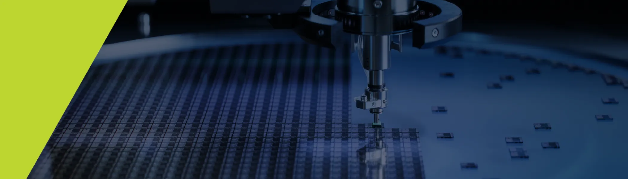
downloadGroupGroupnoun_press release_995423_000000 copyGroupnoun_Feed_96767_000000Group 19noun_pictures_1817522_000000Member company iconResource item iconStore item iconGroup 19Group 19noun_Photo_2085192_000000 Copynoun_presentation_2096081_000000Group 19Group Copy 7noun_webinar_692730_000000Path
Skip to main content
Default Banner Image

Ireland

Registration

For questions or inquiries, please contact: 

Elle Liang

[email protected]

+
Belgium China France Germany India Ireland Italy Japan Malaysia Russia Singapore South Korea Taiwan United States Vietnam 360x317_Event_Calendar_Ad_DAI_Analyzing AI_Driven_v1@2x Business Executive
Highlighted content

The wide adoption of Artificial Intelligence is profoundly impacting many industries, perhaps none more so than the semiconductor industry. Beyond serving as a growth driver for chips across a diverse range of applications, AI and semiconductors are beginning a virtuous cycle where AI is helping to design more powerful chips that in turn enable more advanced AI. The semiconductor industry’s path to $1 trillion in annual revenue by the end of the decade is promising, thanks in large part to AI, but what will that journey actually look like?

This webinar will examine the industry’s AI-driven growth opportunities in depth, while looking at the technological innovation needed to fuel the market expansion. Dr. Handel Jones, CEO of IBS, and author of When AI Rules the World, will share his analysis of how AI will shape the outlook for semiconductor end-markets and segments – along with the race to achieve 1.0nm technology nodes and accelerate the virtuous AI-semiconductor development cycle. He will also cover the future of semiconductor market growth in the AI era as well as areas of opportunities.

About IBS

United States

10:00 am - 10:05 am
Ajit Manocha, SEMI
Ajit Manocha
CEO
SEMI

Welcome Remarks

10:05 am - 10:10 am
Pushkar Apte
Pushkar Apte
Strategic Technology Advisor, Smart Data-AI
SEMI

SEMI Smart Data-AI Initiative and Future of Computing Update

10:10 am - 11:00 am
Handel Jones
Dr. Handel Jones
CEO
IBS

Why AI Will Propel the Semiconductor Market to $1 Trillion and Achieve 1.0nm by 2030

11:00 am - 11:15 am

Q&A

Explore how Artificial Intelligence will impact the semiconductor market through the end of the decade with a deep-dive analysis of the fast-shifting industry landscape focusing in on growth across end markets and segments.

10:00 am - 11:15 am Off Add to Calendar 2024-11-20 10:00:00 2024-11-20 11:15:00 Analyzing AI-Driven Growth: $1T and Beyond Explore how Artificial Intelligence will impact the semiconductor market through the end of the decade with a deep-dive analysis of the fast-shifting industry landscape focusing in on growth across end markets and segments. United States SEMI.org [email protected] America/Los_Angeles public America/Los_Angeles On-demand
Event format
Belgium France Germany India Ireland Italy Japan Malaysia Russia Singapore South Korea Taiwan United States Vietnam Register Now (8-9am PT) Register Now (5-6pm PT) [email protected] Business Executive Featured Speakers
Highlighted content

In today’s fast-paced and interconnected world, the electronics industry faces unprecedented challenges from global disruptions, geopolitical uncertainties, and supply chain vulnerabilities. To remain competitive and resilient, organizations must adopt robust risk management frameworks that proactively identify and mitigate risks.


This webinar is brought to you by the Resiliency Working Group, part of the SEMI Supply Chain Management Initiative. We will explore the creation and implementation of an industry-standard risk management framework tailored to the unique complexities of the electronics supply chain. Attendees will learn how to assess potential risks, develop mitigation strategies, and leverage cutting-edge tools to improve visibility and responsiveness across their supply networks.

Key topics include:


•     The critical risks impacting electronics supply chains and how to address them.
•     Best practices for building a resilient and adaptable risk management framework.
•     Strategies for real-time risk monitoring, supplier risk assessments, and scenario planning.
•     How to align your supply chain with industry standards for business continuity and operational stability.

Who should attend:


•    Supply chain managers
•    Risk officers
•    Operations executives
•    Anyone involved in supply chain planning and resilience in the electronics sector

Join us to discover actionable insights and practical approaches to future-proof your electronics supply chain, ensuring it remains resilient, efficient, and prepared for any disruption.
 

Speaker bio:

Austin Evans is the Director of Supply Chain Risk Management at Intel.  He is responsible for overseeing risk management for Intel’s supply chain as well as Intel’s Contingent Workforce Program Office.  His organization is responsible for business continuity, governance, resilience, supply chain security and compliance. 

United States

Austin Evans.jpg
Austin Evans
Director of Supply Chain Risk Management
Intel
Standards

Join us for a deep dive into the new industry-standard risk management framework tailored to the unique complexities of the electronics supply chain. Hosted by the SEMI Resiliency Working Group, this webinar will equip supply chain professionals with actionable insights on assessing critical risks, developing robust mitigation strategies, and leveraging advanced tools for real-time monitoring.

Off Add to Calendar 2024-10-24 00:00:00 2024-10-24 00:00:00 Building Resilient Supply Chains Join us for a deep dive into the new industry-standard risk management framework tailored to the unique complexities of the electronics supply chain. Hosted by the SEMI Resiliency Working Group, this webinar will equip supply chain professionals with actionable insights on assessing critical risks, developing robust mitigation strategies, and leveraging advanced tools for real-time monitoring. United States SEMI.org [email protected] America/Los_Angeles public America/Los_Angeles
Event format
Belgium China France Germany India Ireland Italy Japan Malaysia Russia Singapore South Korea Taiwan United States Vietnam EMG webinar HI Technical
Highlighted content

Heterogeneous Integration (HI) has come a long way in 50 years. The world of multi-chip modules (MCMs) has given way to a vast ecosystem of chiplets, 3D stacked die, and co-packaging of antenna, high-bandwidth memory (HBM), and optics. HI is at the center of “More than Moore” development activities, as innovative engineers look for creative ways to overcome the slower scaling of silicon technology. The promise of HI is new devices with superior power, performance, area, and cost (PPAC). All these promises come with new challenges. Managing different process nodes, physical characteristics, mechanical stresses, and other system-level challenges not found in monolithic system-on-chip (SoC) devices, creates a great opportunity for design and manufacturing companies to reshape our industry. 


In this webinar, we’ll explore this enabling technology from both the device maker and material supplier perspectives. We will learn about demands placed on devices by new applications and what new tools are needed to meet these demands. We will also hear about the challenges placed on materials and equipment suppliers to develop processes capable of manufacturing the individual components and integrating them into final products. Join us as our panel of experts address the issues and opportunities involved with heterogeneous integration. 
 

United States

Arsalam Alam
Arsalan Alam, PhD
Member of Technical Staff (MTS), 3D Stacking Technology Group
AMD Packaging

2nd Generation 3D V-Cache™ Enablement

Andrea Chacko
Andrea Chacko, PhD
Director of Packaging Solutions
Brewer Science
Dong Shun Bai
Dongshun Bai, PhD
Business Development Director and Senior Technologist of Packaging Solutions
Brewer Science

Enabling Heterogeneous Integration through Material Design

The realization of Heterogeneous Integration (HI) has been key in driving advancements in semiconductor technology. The complexities of integrating dissimilar materials continue to be a challenge for HI. All advanced packaging technologies rely on advanced materials to address the many challenges in achieving continued shrinking and improved performance of devices. Novel materials capable of managing mechanical stresses and increased thermal budgets with strict cleanliness requirements are required for processes such as wafer thinning, fan-out wafer-level packaging, and hybrid bonding. This presentation will highlight how advanced materials can address the growing challenges in the industry.

Andrea Maret
Andrea Maret
Senior Knowledge Manager
Entegris

Webinar Moderator

APHI CAST EHS NBMC Smart MFG SMG Sustainability EMG ESD Alliance FlexTech FOA ITL MSIG SCIS SE&A SiPAT SOI

Dive into the dynamic world of semiconductor materials and discover the future landscape as the industry experts provide a glimpse into the future of the semiconductor ecosystem in the era of heterogenous integration.

10:00 am - 11:00 am Off Add to Calendar 2024-10-16 10:00:00 2024-10-16 11:00:00 Heterogeneous Integration finds its place Dive into the dynamic world of semiconductor materials and discover the future landscape as the industry experts provide a glimpse into the future of the semiconductor ecosystem in the era of heterogenous integration. United States SEMI.org [email protected] America/Los_Angeles public America/Los_Angeles REGISTER NOW
Event format

Chip Integration Technology Center (CITC) today announced the appointment of Toni Versluijs as the new chairman of its Supervisory Board. Versluijs will serve as the incoming chairman from September through December. Effective January 1, 2025, he will take over the responsibilities from chairman Roel Fonville who is retiring.

Versluijs has an extensive background of more than 25 years in the semiconductor industry, of which more than 15 years in general and executive management roles. Prior to this appointment, he worked for NXP, where he led the In-Vehicle Networking product line and was NXP Nijmegen site director and statutory director of NXP Netherlands. Most recently, he led the Business Group MOS at Nexperia, served as statutory director for Nexperia in the UK and was part of the company’s global executive leadership team.

He explains his choice for CITC: “I look forward to using my many years of experience in the semiconductor industry to contribute to the success of CITC in Nijmegen. Nijmegen is a location with a long heritage in semiconductor packages that have changed the world. CITC is a unique venture and has a unique position between private parties, the academic world and knowledge institutes.”

CITC is a smaller and different kind of organization than his previous employers, but Versluijs sees the potential: “CITC has attracted quite some talent in recent years, built partnerships and initiated new developments. In short: it has laid the foundation for growth, and it will flourish in the coming years. I am convinced that it has the potential to change the world of semiconductor packaging again.”

The current chairman of the CITC Supervisory Board, Roel Fonville, adds: “The Supervisory Board is very pleased to welcome Toni Versluijs to our midst. His personality and broad experience in the industry and in the Nijmegen region will help the Board to fulfill its role in securing the continued development of the organization.”

About CITC
Chip Integration Technology Center (CITC) is a non-profit, joint innovation center specializing in heterogeneous integration and advanced chip packaging technology. CITC has created an effective ecosystem in which companies, research and educational institutes work on bridging the gap between academics and industry. CITC's contribution to the ecosystem is to provide access to innovation, infrastructure, and education. CITC was founded in 2019 with strategic partners TNO and Delft University of Technology and is supported by local and regional governments.
www.citc.org

MUNICH, Germany ─ August 19, 2024 Themed Innovation and Collaboration: Powering Sustainable Exponential Growth, SEMICON Europa 2024 will gather industry experts November 12-15 at Messe München in Munich, Germany for insights into the latest innovations and trends in sustainability, mobility, healthcare, materials, packaging, fab management and workforce. Co-located with electronica, SEMICON Europa, Europe’s premier exhibition and conference for the microelectronics supply chain, will feature keynotes from the electronics design and manufacturing ecosystem, academia and governments. Registration is open. 

SEMICON Europa"Leaders from across the value chain at SEMICON Europa will discuss innovations and collaboration strategies that are driving semiconductor industry growth in Europe and globally," said Laith Altimime, president of SEMI Europe. "The industry remains committed to ensuring harmony between technological advancement and environmental progress. We look forward to hosting visionaries as they offer insights into achieving sustainable growth and overcoming the talent gap."

A key highlight of the event, the CxO Summit, will bring together visionary leaders from across the value chain to discuss how Europe’s microelectronics ecosystem can collaborate to uphold strategic leadership. The Summit will serve as a stage for fostering insightful partnerships on pressing and emerging challenges throughout SEMICON Europa. Executives from AMS Osram, Bosch, Comet Group, Inficon, Porsche, Schneider Electric, Siemens, STMicroelectronics, and other leading companies will share insights on the critical issues shaping the foundation for sustainable exponential growth in the European semiconductor industry.

SEMICON Europa 2024 will feature the launch of the III-V Compound Summit that will showcase the critical importance and emerging impact of III-V compound semiconductors in driving the future of electronics.

“Advancements in III-V compound semiconductor materials are crucial for the next generation of high-performance, energy-efficient devices, supporting the industry to overcome manufacturing complexities, boost efficiency and reduce costs,” said Ajit Manocha, SEMI President and CEO. “The III-V Compound Summit at SEMICON Europa will be an indispensable discussion in how these technologies will transform the electronics landscape, marking the beginning of a new era of technological progress.” 

Additional SEMICON Europa Highlights

  • ITF Chip into the Future - Powered by imec: Industry leaders will examine how the EU Chips Act can advance Europe’s semiconductor industry through collaboration, innovation, and investment. Discussions will cover key drivers, best practices, and the future of chip research and manufacturing.
  • Advanced Packaging Conference: Leading experts will discuss innovations in chiplets, heat dissipation, miniaturization, and other advanced packaging techniques essential for meeting the high-performance computing demands of modern AI applications.
  • Fab Management Forum: Presenters will explore strategies to enhance semiconductor manufacturing efficiency and performance. Topics include global market strategies, smart manufacturing, innovations, environmental sustainability, supply chain resilience, and next-gen technologies.
  • MEMS & Imaging Sensors Summit: Sessions will examine how advancements in MEMS and imaging technologies are enhancing connectivity and driving innovation across sectors such as agriculture, automotive, and healthcare, with a focus on the integration of AI/ML and data fusion in next-generation applications.
  • SEMI Networking Night: Industry stakeholders will gather to connect with peers and explore new business partnerships.

Executive Forum Programs 

  • Cultivating a Thriving SiC Market: This session will feature insights from industry leaders addressing the challenges and solutions in Silicon Carbide (SiC) power semiconductors, crucial for automotive and AI applications.
  • Electrification and Power Semiconductors: Examining key innovations in power semiconductors driving global electrification, this session will cover focus areas including efficiency, cost-performance, manufacturing technologies, and the role of semiconductors in advancing sustainable energy and electric vehicles.
  • Global Automotive Advisory Council Summit - Smart Mobility Forum: Addressing current challenges and opportunities in automotive semiconductor technology, this forum will bring together stakeholders and innovators to explore trends, such as autonomous, electric and software defined vehicle, towards a sustainable future in mobility.
  • Innovation Showcase: Attendees will learn about innovations in the microelectronics and semiconductor space.
  • Integrated Photonics: This session will explore how photonic integrated circuits (PICs) are transforming various industries by combining optical and electronic systems into compact, high performance, energy and cost-efficient designs.
  • Meet the SEMIs: Session attendees will have opportunities to network with SEMI European Committee Members, exchange ideas, and discuss ways to advance the industry.
  • Smart Manufacturing: This session will explore AI solutions for smarter semiconductor manufacturing operations, including data acquisition, digital twins, and autonomous production, with a focus on climate. 

TechARENA Programs 

  • 20 Under 30 Recognition Program: The 2024 SEMI Europe 20 Under 30 will honor young leaders in the microelectronics supply chain for their career success, leadership, commitment, community involvement, and collaborative innovation.
  • Advocacy and Geopolitics: Exploring the European Economic Security Strategy's impact on the semiconductor industry, this session will feature presenters discussing how new policies affect global supply chains and the need for international cooperation to ensure competitiveness and long-term growth.
  • Breakthroughs in Medical Technology: This session will explore how advanced medical electronics and semiconductors are advancing digital healthcare for the future.
  • Building the Talent Pipeline – SEMI Initiatives: Session attendees will discover how SEMI initiatives are fostering a robust talent pipeline for the semiconductor industry through university partnerships, STEM outreach, ongoing training, and diversity programs.
  • End-to-End Cybersecurity: Experts will come together to explore comprehensive solutions for securing semiconductor supply chains, protecting intellectual property, and ensuring product integrity in a connected world.
  • EU Digital Forum: Partners from HiCONNECTS and other R&D EU-funded projects will demonstrate how innovative heterogeneous integration (HI) core technologies address major societal and technical challenges.
  • European Projects for a Diverse Talent Pipeline: Speakers will highlight European Commission funded projects under the EU Chips Act aimed at addressing the urgent talent gap in the semiconductor industry by enhancing STEM education, re-skilling and up-skilling, promoting diversity, and sharing best practices in recruitment and onboarding.
  • Future Disruptions: Experts will share actionable insights and strategies on critical topics such as supply chain management, sustainability, ESG, PFAS regulations, and geopolitical impacts to navigate future disruptions in the semiconductor industry.
  • Future of Computing: This session will examine how advancements in quantum computing, neuromorphic computing, and trusted electronics are addressing global challenges and transforming the future of information processing with innovative solutions.
  • Future of Work: Industry leaders will discuss how inclusive leadership can address the global talent shortage, develop the next generation of industry leaders, and foster a diverse and sustainable workforce.
  • Materials Innovation: This session will examine how innovations in materials are advancing Moore’s Law, supporting sustainable semiconductor manufacturing, and addressing global environmental challenges.
  • SCREENInnovation For a Sustainable World: Experts will present updates on new equipment platforms and solutions for Industry 4.0, 3D-Integration, and More-than-Moore devices, drawing from 25 years of collaboration with European partners.
  • Tackling Investment in Semiconductors Start-Ups: This session will feature demonstrations on how European innovations are enabling future technology roadmaps and scaling up start-ups in the industry. 

For more details, please visit the SEMICON Europa 2024 website and connect with SEMI Europe on X or LinkedIn @SEMIEurope (#SEMICONEuropa).

Press and media partners can register for free by contacting Sitong He at [email protected].

SEMICON Europa Sponsors 

About SEMI

SEMI ® is the global industry association connecting over 3,000 member companies and 1.5 million professionals worldwide across the semiconductor and electronics design and manufacturing supply chain. We accelerate member collaboration on solutions to top industry challenges through Advocacy, Workforce Development, Sustainability, Supply Chain Management and other programs. Our SEMICON ® expositions and events, technology communities, standards and market intelligence help advance our members’ business growth and innovations in design, devices, equipment, materials, services and software, enabling smarter, faster, more secure electronics. Visit www.semi.org, contact a regional office, and connect with SEMI on LinkedIn and X to learn more.

Association Contacts

Maria Daniela Perez / SEMI Europe 
Phone: +49 160 2562977 
Email: [email protected]

Samer Bahou / SEMI Headquarters
Phone: +1 408 943 7870
Email: [email protected]

Belgium France Germany Ireland Italy United States Failure Yield Analysis Training
Highlighted content

Course Description 

The Failure Yield Analysis course is an 8-hour webinar held over two days, for 4 hours each day. This course offers an introduction to a variety of effective tools, as well as the overall process flow for locating and characterizing the defect responsible for the failure. Analysts are required to understand a variety of disciplines in order to effectively perform failure analysis. This requires knowledge of subjects like design, testing, technology, processing materials science, chemistry, and even optics. Failed devices and low yields can lead to customer returns and idle manufacturing lines, costing a company millions of dollars a day. This course is designed for every manager, engineer, and technician working in the semiconductor field, using semiconductor components and supplying tools to the industry. 

Course Objectives

  1. This seminar will provide participants with an overview of the tools, techniques, and processes used in failure and yield analysis.
  2. Participants will be able to determine how to proceed with a submitted request for analysis, ensuring that the analysis is done with the greatest probability of success.
  3. The seminar will identify the advantages and disadvantages of a wide variety of tools and techniques that are used for failure and yield analysis.


Course Topics

  • Introduction to Failure Analysis
  • Failure Analysis Principles/Procedures
  • Gathering Information
  • Package Level Testing
  • Electrical Testing
  • Decapsulation/Backside Sample Preparation
  • Die Inspection
  • Photon Emission Microscopy
  • Electron Beam Tools
  • Optical Beam Tools
  • Thermal Detection Techniques
  • Chip-Level Deprocessing
  • Analytical Techniques
  • Probing
  • Focused Ion Beam Technology


Chris Henderson 

Semitracks, Inc. 

Instructor Bio

Important Information

Note that only the person who registered will receive a certificate of completion. This virtual training will not be recorded. Attendees must be present to access course knowledge. 

Can't find the training link day of? After you register, you will receive the link to the live training via the email address you provided. In addition, you will receive email reminders about 24 hours in an advance and an hour before with the same link. Please keep these emails on hand to access the trainings on time. If you do not see any confirmation emails, please check your junk/spam folders before contacting SEMI U for support.

United States

- SEMI U

The Failure Yield Analys course is an 8-hour webinar that is held for 4 hours each day. 

Pricing
  • Members: $599
  • Non-Members: $649
  • Students/Vets: $549

* For group orders with 10+ attendees, and for Students/Veterans, discounted pricing, please contact [email protected].

8:00 am - 12:00 pm Off Add to Calendar 2026-07-27 08:00:00 2026-07-28 12:00:00 Failure Yield Analysis (Americas/EU) The Failure Yield Analys course is an 8-hour webinar that is held for 4 hours each day. PricingMembers: $599Non-Members: $649Students/Vets: $549* For group orders with 10+ attendees, and for Students/Veterans, discounted pricing, please contact [email protected]. United States SEMI.org [email protected] America/Los_Angeles public America/Los_Angeles Register Now
Event format
Promote in calendar
Off

Axiomise, a company noted for enabling formal verification adoption, today announced the formation of its Technical Advisory Board and its first two members, Dr. Vidya Chandran Darbari and Colin McKellar.

Dr. Darbari is an Axiomise co-founder and company director as well as Senior Lecturer in Structural Biology at Queen Mary University of London (QMUL). McKellar, formerly Vice President of Imagination Technologies, is currently Senior Director of Hardware at X-Silicon Inc.

“Vidya and Colin have long served as my unofficial advisers and confidants as I built Axiomise from the ground up,” remarks Dr. Ashish Darbari, founder and CEO of Axiomise. “Formalizing our relationships with Vidya and Colin will further strengthen the company and the expertise of our formal verification experts.”

“I have had the pleasure of watching Axiomise grow from early startup to a formidable verification provider and I couldn’t be prouder,” states Dr. Darbari. “I look forward to adding my voice as a member of the Technical Advisory Board.

My relationship with Ashish goes back to the early days of Imagination,” notes McKellar. “I watched with amazement and respect as he implemented a rigorous formal verification flow that caught bugs that would have forced costly respins and threats to the company’s good name and reputation.”

About Dr. Vidya Chandran Darbari
Dr Vidya Chandran Darbari, an Axiomise co-founder and company director, has a multi-disciplinary record combining medicine, life sciences, mathematics and technology. A leader and key contributor who leads from the front, Dr. Darbari helped steer Axiomise from its early stages to establishing it as a global leader in formal verification consulting and services, training and RISC-V solutions. She is a senior lecturer at the Queen Mary University of London with several impactful publications in high-end journals including Nature and Science. Dr Darbari received her Bachelor of Medicine, Bachelor of Surgery (MBBS) degree from Seth G.S. Medical College (KEM Hospital) in Mumbai, India, before completing her Master of Technology (MTech) degree from Indian Institute of Technology (IIT) Bombay. Dr. Darbari obtained her Doctorate degree from the University of Cambridge. She has been recognized for her innovative research through Biochemical Society Early Career Award, British Crystallographic Society Early Career prize and recently a Research Excellence Award by the Science and Engineering Faculty at QMUL.

About Colin McKellar
Colin McKellar brings the customer experience to the Axiomise team having been a key player in driving customer engagements in his previous roles with Apple, Intel, TI, SiFive and SEGA among others. He started his career in electronics 30 years ago in Sony Broadcast and Professional working on HD video encode and decode. Most of his career was spent working at Imagination Technologies as a key contributor to the graphics IP roadmap and was instrumental in bringing in and maturing a world-class verification infrastructure including simulation, formal verification and large FPGA, emulation and silicon farms. McKellar joined X-Silicon in 2023 with the responsibility to drive product and execution for bringing graphics and AI acceleration to the RISC-V ecosystem. He has a wealth of design and verification experience across GPU, CPU, AI and SoC chips successfully managing large multinational teams of more than 200 engineers.

About Axiomise
Axiomise is accelerating formal verification adoption through its unique combination of training, consulting, services and specialized verification solutions for RISC-V. Axiomise was founded by Dr. Ashish Darbari, FBCS, FIETE, DPhil (Oxford), who has been a formal verification practitioner for more than two decades with 60 patents in formal verification and over 70 publications.

Engage with Axiomise at:
Website: www.axiomise.com
Twitter: @axiomise
LinkedIn: https://www.linkedin.com/company/axiomise/
Facebook: https://www.facebook.com/axiomise

Sunnyvale, USA - Meylan, FRANCE – May 29, 2024 Numem - a leader in high-performance Memory IP Cores and Memory Chip/Chiplet based on its patented NuRAM (MRAM) and SmartMem technologies, and IC’ALPS - a leader in ASIC/SoC design and supply chain management, have pooled their expertise to meet the challenge of developing an ambitious integrated circuit with RISC-V processors, 2MBytes of NuRAM and a DSP/AI Custom Datapath Accelerator. The Custom SoC was developed in an advanced technology node.

This SoC has been designed and implemented to highlight the Numem high-performance, low power Memory subsystem with a RISC V Processor and AI Accelerator for ultra-low power applications. It has been developed through a close collaboration between Numem and IC’ALPS.

The physical implementation of this integrated circuit was made in a secure space (isolated location, network, and servers, encrypted exchanges, etc.) to meet with the stringent protection of sensitive data required by this program.

“We were very pleased with the collaboration and quality of service provided by IC’ALPS which made this on-time tape out possible and first time functional silicon,” said Jack Guedj, CEO of Numem. NuRAM with SmartMem is a high-performance memory subsystem which is 2-3x smaller and boast significant power reduction over SRAM,” he added.

Lucille Engels, COO of IC’ALPS indicated: “The challenges were numerous including: architecture, power domains, protection of the sensitive data, run times pushing improvement of EDA flow and the pressure of the tape out deadline.”

Numem and IC’Alps intend to extend their partnership to serve new customers SoC projects – feel free to contact us.

NUMEM/IC'ALPS with ultra-low-power SoC for Sensor and AI

About NUMEM
Numem, headquartered in Sunnyvale, California, is the leading provider of Memory Subsystem Chip/Chiplet and IP based on proven foundry MRAM process. Numem’s patented NuRAM technology enables best in class power/performance and reliability with 2.5x smaller area and 85x lower leakage power than traditional SRAM. Numem’s SmartMem subsystem technology significantly improves performance and endurance as well as ease-of-use and reliability for high-volume deployment and enables to reach ultra-high bandwidth.
Visit our website at https://www.numem.com or contact us at [email protected].

About IC’Alps
IC’Alps is your one-stop-shop ASIC partner. Based in France (HQ in Grenoble, two design centers in Grenoble and Toulouse), the company provides customers with a complete offering for Application Specific Integrated Circuits (ASIC) and Systems on Chip (SoC) development from circuit specification, mastering design in-house, up to the management of the entire production supply chain. Its areas of expertise include analogic, digital and mixed-signal circuits (sensor/MEMS interfaces, ultra-low power consumption, power management, high-resolution converters, high voltage, signal processing, ARM and RISC-V based multiprocessors architectures, hardware accelerators) on technologies from 0.18 µm down to 5 nm, and from multiple foundries (TSMC, Global Foundries, Tower Semiconductor, X-FAB, STMicroelectronics, etc.). The company is active worldwide in medical, industrial, automotive, IoT, IA, mil-aero and digital identity & security sectors. IC’Alps is ISO 9001:2015, ISO 13485:2016, EN 9100:2018 certified, Common Criteria on-demand, IATF16949-ready, member of TSMC Design Center Alliance (DCA), ARM Approved Design Partner and X-FAB’s partner network. More information on www.icalps.com and follow us on https://www.linkedin.com/company/ic-alps

Belgium France Germany Ireland Italy United States FEMC 23 tile with NBMC Postponed.jpg Business Executive
Highlighted content

Your company has built a strong patent portfolio — now what? This webinar will discuss strategies for managing existing patents, including how to use IP to strengthen your business and maximize return on investment.  Topics will include best practices for patent marking, controlling rising maintenance fees, and licensing, as well as insights into emerging trends in patent enforcement and litigation in the semiconductor sector.


 ABOUT THE SPEAKER

Michael Jones, Partner, Rothwell Figg
Michael H. Jones’s practice includes patent litigation, patent prosecution, and IP counseling.  Michael advises clients who have developed a broad range of technologies, including semiconductor devices and manufacturing, integrated circuits and systems, green energy, terahertz electronics, hardware and protocols for wireless communications, and various online technologies. Although much of his work is with large multinational clients with complex patent portfolios, Michael also has a significant, and growing, practice with smaller high-technology clients, ranging from startups to growth companies dealing with patent issues for the first time in their evolution. Michael has a B.S. in Electrical and Computer Engineering from University of Virginia, a M.S. in Electrical and Computer Engineering from University of California, Santa Barbara, and a J.D. from The George Washington University Law School.

United States

Michael Jones
Michael Jones
Member
Rothwell Figg
Gity Samadi
Gity Samadi
Director, R&D Programs
SEMI
NBMC ESD Alliance FlexTech 10:00 am - 12:00 pm Off Add to Calendar 2024-11-06 10:00:00 2024-11-06 12:00:00 FEMC #23 Best Practices for Semiconductor Patent Portfolio Management United States SEMI.org [email protected] America/Los_Angeles public America/Los_Angeles
Event format
Belgium France Germany Ireland United States Register Now EAGS Image Business Executive Featured Speakers
Highlighted content

United States

Michael Doescher NXP
Michael Doescher
NXP
Mani Goswami, DuPont
Manibarsha Goswami
DuPont
Wojtek Lam
Wojtek Osowiecki
Lam Research
Justin Harris, CEC SEMI
Justin Harris
SEMI / Climate Equity Collaborative
Sustainability Workforce Development

Join this webinar to find out how companies across the semiconductor value chain are prioritizing employee-driven climate action and social impact,. Hear how employee-driven initiatives are enhancing sustainability and equity -- and gain ideas on how you and your organization might benefit.

With the Paris Climate Agreement and growing awareness of the climate crisis, many people are asking "how can I contribute in my private and professional life?"  

This Employee Action Workshop, organized by the Climate Equity and Social Impact (CESI) workgroup of SEMI will focus on setting up sustainability-based employee groups within your company. How to engage speakers and attendees, and the resources that exist to help.  

We will show you how to create an in-house, bottom-up sustainability network and offer concrete ideas for action. Industry leaders will share their experiences and successes, providing valuable insights into volunteerism, ESG innovation, and impactful employee initiatives.

For anyone who wants to use your biggest multiplier - your workplace - to make a difference in Climate Change.

This webinar takes place 8:00 AM - 9:00 AM Pacific Time Zone

8:00 am - 9:00 am Off Add to Calendar Disabled America/Los_Angeles
Event format