downloadGroupGroupnoun_press release_995423_000000 copyGroupnoun_Feed_96767_000000Group 19noun_pictures_1817522_000000Member company iconResource item iconStore item iconGroup 19Group 19noun_Photo_2085192_000000 Copynoun_presentation_2096081_000000Group 19Group Copy 7noun_webinar_692730_000000Path
Skip to main content
Default Banner Image

Germany

ESG progress, industry-first sustainability leadership and long-term governance goals

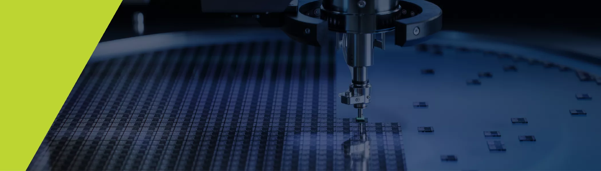
Rolla, Mo. — June 2, 2026 — Brewer Science, a global leader in developing and manufacturing next-generation materials and technologies for the semiconductor industry, today released its 2026 Impact Report, detailing continued progress across environmental stewardship, people-first initiatives, community engagement, and collaborative innovation. Additionally, the company announced it has earned GreenCircle Certified Zero Waste to Landfill certification for the eleventh consecutive year, remaining the first and only company in the semiconductor and microelectronics industry to achieve this designation.

Explore Brewer Science’s 2026 Impact Report

“The consistency matters,” said Matthew Beard, Executive Director of Strategic Planning, Management Systems, and Sustainability at Brewer Science. “Eleven consecutive years of Zero Waste to Landfill certification demonstrates our commitment to improving our processes, finding more innovative ways to reduce, reuse, and recycle our waste, thus leading to more sustainable business operations and having a positive impact on our supply chain.”

Environmental leadership rooted in verification and results

The 2026 Impact Report highlights continued momentum toward Brewer Science’s climate and waste-reduction goals, including:
• More than 631 tons of material diverted from landfills over the past decade
• 56% of generated waste reused or recycled during the most recent reporting period
• Over 75% of hazardous waste volume diverted annually to reuse applications
• 100% renewable energy consumption achieved annually
• 5% reduction in Scope 3 greenhouse gas emissions year over year
• Continued progress toward reducing Scope 1 and Scope 2 emissions by 80% by 2030 (from a 2018 baseline) and achieving net-zero carbon emissions by 2050

Brewer Science’s Zero Waste to Landfill certification verifies that 100% of waste leaving company facilities is diverted through approved methods such as reuse, recycling, composting, or source reduction. GreenCircle Certified’s program is widely regarded as one of the most rigorous third-party validations of waste diversion claims.

People, community, and industry impact

Beyond environmental performance, the Impact Report details how Brewer Science’s sustainability commitments extend to its workforce, communities, and industry partnerships:
• Named a Top Workplace in the Manufacturing Industry for the fifth consecutive year
• Employee-owners volunteered more than 3,200 hours to 129 organizations
• Supported STEM education, early childhood education, and workforce development initiatives across local and national communities
• Continued leadership as a founding member of the Semiconductor Climate Consortium, collaborating with peers to reduce emissions across the global semiconductor supply chain
• Ongoing innovation in PFAS free materials development, aligning product performance with environmental responsibility

A platform for collaboration and accountability
The 2026 Impact Report also highlights Brewer Science’s Sustainability Outreach Program, which provides tools and education for employees, customers, suppliers, and community partners to drive meaningful, scalable environmental action.

“Zero waste is not a finish line, it’s a responsibility we share,” Beard added. “We encourage our partners across the supply chain to align around verified sustainability standards and measurable impact.”

The full 2026 Impact Report is available on Brewer Science’s Going Green page at:
www.brewerscience.com/going-green

About Brewer Science
Brewer Science is a global leader in developing and manufacturing next-generation materials and processes that enable cutting-edge technology. Since 1981, the company has expanded its technology portfolio within advanced lithography, advanced packaging, smart devices, and printed electronics to support microdevices and industrial monitoring solutions. Brewer Science’s relationship-focused approach ensures critical outcomes for its partners worldwide. Headquartered in Rolla, Missouri, Brewer Science operates globally. Learn more at www.brewerscience.com.

About GreenCircle Certified, LLC
GreenCircle Certified, LLC provides independent, third-party certification of environmental claims to ensure transparency and credibility in the marketplace. Since 2009, GreenCircle Certified has helped organizations validate sustainability performance through rigorous evaluation. Its certifications, including Zero Waste to Landfill, are accredited by the ANSI National Accreditation Board (ANAB). Learn more at www.greencirclecertified.com.

###

SEMI Members:  $75

Use your corporate email address during log in to be recognized as a SEMI Member.

Non-Members:  $149

Students:  Free

Contact Basak Ulutas Ozturkler ([email protected]) with a picture of your student ID to receive your discount code.

Belgium Germany Singapore Taiwan United States FEMC30 Business Executive Technical
Highlighted content

High-temperature materials are critical for applications in harsh-environment circuitry, where devices must operate reliably under extreme thermal, chemical, and mechanical stress. In this Master Class, Dr. Shenqiang (Shen) Ren will present a high-throughput ink materials development strategy enabled by non-equilibrium processing and hybrid additive manufacturing. This approach enables rapid synthesis, combinatorial screening, and direct integration of functional materials onto diverse substrates. The resulting materials exhibit strong electrical performance, robust adhesion, and long-term stability under harsh operating conditions. This high-throughput framework accelerates the discovery and deployment of printable materials for interconnects, heaters, and EMI shielding, providing a versatile pathway toward next-generation printed electronics designed for extreme environments.

ABOUT THE SPEAKER

Shenqiang (Shen) Ren, PhD
Dr. Shenqiang Ren is a Professor of Materials Science and Engineering at the University of Maryland, College Park, with research interests in emerging functional and structural materials. He received his Ph.D. in Materials Science and Engineering from the University of Maryland, College Park, and subsequently completed postdoctoral training at the Massachusetts Institute of Technology (MIT). 

United States

Shenqiang Ren
Shenqiang (Shen) Ren , PhD
Department of Materials Science and Engineering, Professor
University of Maryland, College Park
Gity Samadi
Moderator
Gity Samadi, PhD
Sr. Director, R&D Programs
SEMI
NBMC Smart MedTech FlexTech

Join us for a focused Master Class with Dr. Shenqiang (Shen) Ren, exploring the development of high‑temperature materials for harsh‑environment printed and flexible hybrid electronics (FHE). This session will examine how devices can be engineered to operate reliably under extreme thermal, chemical, and mechanical stress—conditions where conventional materials and processes often fail.

The Master Class will also highlight how this high‑throughput framework accelerates the discovery and deployment of printable materials for interconnects, heaters, and EMI shielding, offering a versatile pathway toward next‑generation printed electronics designed for extreme conditions.

10:00 am - 12:00 pm Off Add to Calendar 2026-08-26 10:00:00 2026-08-26 12:00:00 FEMC#30 High Throughput Material Development for Extreme Environment Printed Electronics Join us for a focused Master Class with Dr. Shenqiang (Shen) Ren, exploring the development of high‑temperature materials for harsh‑environment printed and flexible hybrid electronics (FHE). This session will examine how devices can be engineered to operate reliably under extreme thermal, chemical, and mechanical stress—conditions where conventional materials and processes often fail.The Master Class will also highlight how this high‑throughput framework accelerates the discovery and deployment of printable materials for interconnects, heaters, and EMI shielding, offering a versatile pathway toward next‑generation printed electronics designed for extreme conditions. United States SEMI.org [email protected] America/Los_Angeles public America/Los_Angeles REGISTER NOW
Event format
Promote in calendar
Off
Belgium France Germany Ireland Italy Overview 9/15 Training

Course Description

This course offers a solid foundation in semiconductor manufacturing, from basic concepts to advanced techniques, providing practical insights into the tools, processes, and technologies driving the industry.

Learning Objectives

  • Gain a comprehensive understanding of the semiconductor industry and manufacturing process, design, and eco-system of the semiconductor industry
  • Understand the jargon, tools, and materials used in the design and fabrication of an integrated chip
  • Effectively be able to communicate semiconductor manufacturing concepts with other associates and industry professionals

Course Topics

  • Basic Electronics and Microelectronics: Definitions of essential electronic terms/concepts and introduction to microelectronics and integrated circuits
  • Process Nodes: Process nodes and their impact on device performance and cost
  • Device Physics and Transistor Operation: Principles of device operation and transistor functionality
  • Crystal Growth and Wafer Preparation: Crystal growth techniques and wafer preparation processes
  • Advanced Transistor Technologies: FDSOI, FinFETs, and Gate-All-Around (GAA) transistors and their impact on device performance
  • Circuit Design and Layout: Introduction to circuit design, layout techniques, and tools
  • Wafer Processing: Mask Making and Lithography: Techniques and materials used in mask making and various lithographic methods (DUV, Immersion, EUV)
  • Clean Room Environments: Importance of clean rooms in semiconductor manufacturing and contamination issues
  • Etching and Cleaning Processes: Plasma and wet etching processes
  • Ion Implantation and Diffusion Techniques: Methods for doping and controlling diffusion in semiconductor fabrication
  • Deposition Techniques: RTP, CVD, ALD, and ALE techniques and their effect on device performance
  • Electroplating and Sputtering: Metal deposition techniques used in manufacturing
  • Packaging and Testing: Techniques such as wire bonding, die stacking, flip chip, and chiplets packaging, semiconductor testing processes
  • Metrology and Measurement Tools: Tools and methods used for precision measurement in semiconductor manufacturing
  • Semiconductor Industry Ecosystem: The major players in the industry 

Who Should Attend

Anyone interested in understanding semiconductor manufacturing, including new employees, professionals in related industries, and those seeking to broaden their knowledge of the field.

Instructor

Denny Frye 

PT International, LLC

Instructor Bio
 

Testimonials 

See what course participants had to say about this course!

  • "The expansive width of coverage with sufficient depth; well curated, relevant information with live references, and the open style of delivery which made the course more of a sharing than a lecture, was enjoyable."
  • "Denny's knowledge and ability to explain things in simplified ways was awesome!"
  • "I really enjoyed going over the topics and watching the in-depth videos. I also liked how we received the slide information prior to the class."
  • "The range of topics was perfect for an intro course."
  • "Denny did a great job explaining complex topics. The opportunity to ask questions directly was beneficial for the entire class. If a question couldn't be answered immediately, it was addressed by the next break at the latest."
  • "Thank you very much for the informative course. I appreciate the in-depth and in-detail insight in all aspects of Semiconductor Manufacturing!"

Important Information

Note that only the person who registered will receive a certificate of completion. This virtual training will not be recorded. Attendees must be present to access course knowledge. 

Can't find the training link day of? After you register, you will receive the link to the live training via the email address you provided. In addition, you will receive email reminders about 24 hours in an advance and an hour before with the same link. Please keep these emails on hand to access the trainings on time. If you do not see any confirmation emails, please check your junk/spam folders before contacting SEMI U for support. 

Germany

- SEMI U

Gain a comprehensive understanding of the semiconductor industry and the integrated circuit (IC) manufacturing process. This course is designed for new personnel in the field or anyone seeking a well-rounded knowledge of the tools, materials, and terminology used in semiconductor manufacturing.

Pricing

Early Bird Special - $100 off  

  • Members: $995 $895
  • Non-Members: $1095 $995

* Group pricing for up to 20+ attendees: $12,900
Any questions, please contact [email protected]

8:00 am - 5:00 pm Off Add to Calendar 2026-09-15 08:00:00 2026-09-16 17:00:00 Overview of Semiconductor Manufacturing (Europe) Gain a comprehensive understanding of the semiconductor industry and the integrated circuit (IC) manufacturing process. This course is designed for new personnel in the field or anyone seeking a well-rounded knowledge of the tools, materials, and terminology used in semiconductor manufacturing.PricingEarly Bird Special - $100 off  Members: $995 $895Non-Members: $1095 $995* Group pricing for up to 20+ attendees: $12,900Any questions, please contact [email protected] Germany SEMI.org [email protected] Europe/Berlin public Europe/Berlin Register Now
Event format
Promote in calendar
Off
Belgium France Germany Ireland Italy Understanding Training

Course Description

The first part of the course provides a brief overview of semiconductor design and fabrication steps, encompassing IC design techniques, all wafer processing steps, assembly, and packaging. It delves into semiconductor jargon in laypeople terms, and various substrate types such as Si, SiGe, FDSOI, GaAs, SiC, GaN. Additionally, it discusses different types of transistors like pMOS, nMOS, Bipolar, BiCMOS, CMOS, FinFets, and GAA and their evolution and what applications they are used in.
 
The second part of the course focuses on semiconductor business aspects such as silicon economics, wafer processing costs, semiconductor revenue forecasts, driving forces in the industry, top semiconductor IDMs, market competitors based on market share, OEMs, foundries, top tool vendors, and Fabless companies.  Addresses the fastest-growing semiconductor markets based on geographic locations and applications, identifies semiconductor competitors/customers, and discusses major semiconductor markets like Automotive, PC, Mobile, Memory, Wireless, Cell phones, Consumer, Gaming, AI, IoT, Digital TV, Radio, Automotive, MEMS, and Emerging Technology & Impact on Industry.

Learning Objectives

  • Understand the fundamental principles and theories semiconductor technology.
  • Communicate with other associates and understand wafer processing steps.
  • Understand semiconductor business aspects such as silicon economics, wafer processing costs, semiconductor revenue forecasts, driving forces in the industry, top semiconductor IDMs, market competitors based on market share, OEMs, foundries, top tool vendors, and Fabless companies.
  • Review the semiconductor eco-system as it relates to design and fabrication of a semiconductor device.
  • Gain knowledge of major semiconductor markets like Automotive, PC, Mobile, Memory, Wireless, Cell phones, Consumer, Gaming, AI, IoT, Automotive, MEMS, and Emerging Technology & Impact on Industry.
  • Demonstrate effective communication skills through written reports, presentations, and discussions related to semiconductor subjects.
  • Collaborate effectively with peers in group projects or discussions regarding semiconductor subjects.
  • Analyze and evaluate research literature in semiconductor technology.
  • Develop critical thinking and problem-solving skills applicable to semiconductor technology.

Who Should Attend

This course is suitable for anyone seeking a better understanding of the semiconductor industry, market leaders, terminology, business, and the semiconductor ecosystem.

Instructor

Denny Frye 

PT International, LLC

Instructor Bio
 

Testimonials 

See what course participants had to say about this course!

  • "Denny Frye knows so much about the history of the semiconductor industry that he was able to tie together many different industries and technologies that I have heard about but never knew how they were connected."
  • "Great overview of the semiconductor industry & market."
  • "This was a very detailed course on many facets of the industry, would recommend!"
  • "It was a great mix of technical and overview of the key players in the market!"
  • "Good blend on technical and commercial topics."
  • "Excellent introduction to the semiconductor world."
  • "Great session on the understanding of the semiconductor industry in a nutshell."

Important Information

Note that only the person who registered will receive a certificate of completion. This virtual training will not be recorded. Attendees must be present to access course knowledge. 

Can't find the training link day of? After you register, you will receive the link to the live training via the email address you provided. In addition, you will receive email reminders about 24 hours in an advance and an hour before with the same link. Please keep these emails on hand to access the trainings on time. If you do not see any confirmation emails, please check your junk/spam folders before contacting SEMI U for support. 

Germany

SEMI U

Embark on a journey through semiconductor design, manufacturing, and business in this illuminating course. Explore IC design techniques, transistor evolution, and market dynamics. Delve into substrate types and industry economics, discovering the fastest-growing markets and key players shaping the semiconductor landscape.

Pricing

Early Bird Special - $100 off 

  • Members: $845 $745
  • Non-Members: $945 $845

* Group pricing for 20 attendees: $9900
Any questions, please contact [email protected]  

8:00 am - 5:00 pm Off Add to Calendar 2026-09-14 08:00:00 2026-09-14 17:00:00 Understanding Semiconductor Technology and Business (Europe) Embark on a journey through semiconductor design, manufacturing, and business in this illuminating course. Explore IC design techniques, transistor evolution, and market dynamics. Delve into substrate types and industry economics, discovering the fastest-growing markets and key players shaping the semiconductor landscape.PricingEarly Bird Special - $100 off Members: $845 $745Non-Members: $945 $845* Group pricing for 20 attendees: $9900Any questions, please contact [email protected]   Germany SEMI.org [email protected] Europe/Brussels public Europe/Brussels Register Now
Event format
Promote in calendar
Off
Belgium France Germany Ireland Italy United States Plasma Etching 8/25 Training

Course Description

The instructor discusses the applied aspects of plasma-assisted etching from a general point of view. The emphasis is on mechanistic understanding. The etching of Si and its compounds is covered in detail. The chemistries used in the etching of other technology-related materials such as Al, organics, and III-V compounds are summarized. Other topics presented include selectivity, loading, ARDE and feature scale problems, damage, and issues associated with high-density plasma RIE. A section on plasma diagnostics and ion-beam based etching methods is briefly discussed. 

Learning Objectives

  • Understand the fundamentals of dry etching and the basic concepts of plasma etching
  • Understand the physics of rf glow discharges (both high and low density)
  • Understand the surface science aspects of RIE including the role of energetic ions
  • Recognize the factors which influence etching anisotropy
  • Define the steps of plasma-surface chemistry leading to etching

Topics Covered

  • Fluorocarbon plasma etching of Si and its compounds
  • Selectivity, loading effects, and aspect ratio dependent etching
  • Uniformity of etching, damage, feature charging issues, and particles
  • Etching of other materials (Al, organics, III-V compounds, etc)
  • Plasma diagnostics such as optical emission spectroscopy with actinometry, mass spectrometry and laser-induced fluorescence
  • Issues in high density plasma etching, wall effects, and ion beam-based methods
  • Deep Reactive Ion Etching (DRIE)
  • Applications and processing etching using ALE
  • End point detection

Who Should Attend

This course is intended for scientists, technicians and others working with or interested in the dry etching of materials in reactive gas glow discharges, particularly those who do not have extensive experience in the field. 

Instructor

Richard Beaudry

PT International, LLC

Instructor Bio
 

Testimonials

See what previous course participants had to say about this training!

  • "Instructors' Process and Hardware knowledge were impressive."
  • "I finally gained a clear understanding of the RIE process."
  • "The instructor had a very good knowledge of the content."
  • "I had a great time to learn fundamental concepts of plasma etching course from SEMI."
  • "The aspect of the course that I found most beneficial was the Bosch processing parameter discussions on profile management. This subject was clearly the expertise of the presenter who skillfully addressed my questions regarding the subject."

Important Information

Note that only the person who registered will receive a certificate of completion. This virtual training will not be recorded. Attendees must be present to access course knowledge. 

Can't find the training link day of? After you register, you will receive the link to the live training via the email address you provided. In addition, you will receive email reminders about 24 hours in an advance and an hour before with the same link. Please keep these emails on hand to access the trainings on time. If you do not see any confirmation emails, please check your junk/spam folders before contacting SEMI U for support.

United States

- SEMI U

This course discusses the fundamentals of plasma assisted phenomena and reactive ion etching (RIE) processes. The emphasis is on the physical and chemical processes that determine the consequences of a reactive gas plasma/surface interaction. The role of energetic ions as encountered in RIE systems is discussed in detail and the factors which influence anisotropy of etching are highlighted. Plasma-assisted etching equipment is described including capacitively coupled, inductively coupled and wave-generated plasmas sources. 

Pricing
  • Members: $745
  • Non-Members: $845

* * Group pricing for up to 20 attendees: $9900
Any questions, please contact [email protected]

8:00 am - 12:00 pm Off Add to Calendar 2026-08-25 08:00:00 2026-08-26 12:00:00 Plasma Etching, ALE, & RIE (Americas & EU) This course discusses the fundamentals of plasma assisted phenomena and reactive ion etching (RIE) processes. The emphasis is on the physical and chemical processes that determine the consequences of a reactive gas plasma/surface interaction. The role of energetic ions as encountered in RIE systems is discussed in detail and the factors which influence anisotropy of etching are highlighted. Plasma-assisted etching equipment is described including capacitively coupled, inductively coupled and wave-generated plasmas sources. PricingMembers: $745Non-Members: $845* * Group pricing for up to 20 attendees: $9900Any questions, please contact [email protected] United States SEMI.org [email protected] America/Los_Angeles public America/Los_Angeles Register Now
Event format
Promote in calendar
Off
Belgium China France Germany India Ireland Italy Japan Malaysia Singapore South Korea Taiwan United States Vietnam Download the white paper Cost Benefit Calc cropped for events page Business Technical Training
Highlighted content

SEMI
United States

9:00 am - 9:15 pm
Peilun Sun headshot
Peilun Sun
Consortium Manager
SEMI

Setting the Stage: Industry Drivers & SCC Initiative Context

• Semiconductor Industry Decarbonization Challenges
• The Need for Quantified Business Cases
• SCC Initiative Background & Development Journey
• Vision for Industry Adoption & Collaboration

9:16 am - 9:34 am
Ben Gross Headshot
Ben Gross
Director DTMS - Sustainability
Applied Materials

SCC Cost-Benefit Calculator Overview & Walkthrough

• Tool Architecture & Methodology
• Key Inputs & Assumptions
• Understanding the Outputs & Metrics
• Live Demonstration & Example Scenario
• Current Limitations & Future Development Opportunities

9:36 am - 9:50 am
Jeff Rudnik Headshot
Jeff Rudnik
Director of Environmental Sustainability & Net Zero
ASM

Industry Use Cases & Practical Applications

• Evaluating Decarbonization Projects
• Comparing Alternative Mitigation Strategies
• Supporting Internal Investment Decisions
• Lessons Learned from Early Applications
• Opportunities for Industry Collaboration

9:51 am - 10:00 am

Open Discussion & Q&A

• Audience Questions
• Feedback & Enhancement Opportunities
• Next Steps & SCC Engagement Opportunity

Smart MFG Sustainability

The semiconductor industry is under increasing pressure to decarbonize its operations, particularly with regard to Scope 1 emissions — direct greenhouse gas emissions (GHG) from owned or controlled sources. Yet many companies face a persistent challenge: how to make a clear, consistent, and financially credible case for emissions reduction investments. To help address this need, the Semiconductor Climate Consortium (SCC) has developed a Cost-Benefit Calculator — a simplified and flexible tool that offers a structured starting point for evaluating carbon emissions reduction projects. The calculator enables users to estimate the Net Present Cost (NPC) per ton of CO₂ equivalent emissions reduction, helping to translate environmental impact into business-relevant terms.

Join the SEMI's Semiconductor Climate Consortium (SCC) Scope 1 Working Group and document authors for a webinar discussing their journey creating the Cost-Benefit Calculator and outlining the use cases for this tool.  The Cost-Benefit Calculator is a functional spreadsheet with built in report creation tools. For business managers who need to calculate emissions for Scrope 1.

SCC members can download the Cost Benefit Calculator Report here.

9:00 am - 10:00 am Off Add to Calendar 2026-06-16 09:00:00 2026-06-16 10:00:00 SCC: Cost Benefit Calculator Webinar The semiconductor industry is under increasing pressure to decarbonize its operations, particularly with regard to Scope 1 emissions — direct greenhouse gas emissions (GHG) from owned or controlled sources. Yet many companies face a persistent challenge: how to make a clear, consistent, and financially credible case for emissions reduction investments. To help address this need, the Semiconductor Climate Consortium (SCC) has developed a Cost-Benefit Calculator — a simplified and flexible tool that offers a structured starting point for evaluating carbon emissions reduction projects. The calculator enables users to estimate the Net Present Cost (NPC) per ton of CO₂ equivalent emissions reduction, helping to translate environmental impact into business-relevant terms.Join the SEMI's Semiconductor Climate Consortium (SCC) Scope 1 Working Group and document authors for a webinar discussing their journey creating the Cost-Benefit Calculator and outlining the use cases for this tool.  The Cost-Benefit Calculator is a functional spreadsheet with built in report creation tools. For business managers who need to calculate emissions for Scrope 1.SCC members can download the Cost Benefit Calculator Report here. SEMI United States SEMI.org [email protected] America/Los_Angeles public America/Los_Angeles Register Today!
Event format
Promote in calendar
Off

Registration

SEMI Members: $25
Use your corporate email address during log in to be recognized as a SEMI Member.

Non-Members: $50

Students: Contact Paul Cohen ([email protected]) for student pricing.

Germany Taiwan United States ESDA Savage on Security 3 360.jpg Technical
Highlighted content

Designing functionally correct, high-performance, and provably secure system-on-chips (SoCs) has become a strategic imperative for modern computing infrastructure. Yet traditional design and verification methodologies are increasingly strained by escalating complexity, massive design scales, heterogeneous integration, and rapidly evolving security threats. Ensuring correctness, scalability, comprehensiveness, and adaptability across the full SoC lifecycle now exceeds the practical limits of conventional toolchains and human-centric workflows.

The emergence of large language models (LLMs) introduces a transformative opportunity for SoC design automation. Beyond natural language understanding and code generation, advanced LLMs demonstrate capabilities in architectural reasoning, specification refinement, vulnerability analysis, and design-space exploration. However, monolithic models alone are insufficient for the multidisciplinary and iterative nature of chip design. An agentic paradigm—where specialized LLM-driven agents collaborate within a coordinated framework—enables modular reasoning, cross-layer verification, security validation, and adaptive decision-making throughout the design process.

This talk will present a multi-agent intelligent assistant system architected to automate and augment SoC design and security verification. The framework integrates design synthesis, threat modeling, formal reasoning, runtime monitoring strategies, and hardware–software co-verification into a cohesive workflow. Looking ahead, such agentic systems point toward a future of self-optimizing, security-aware, and continuously verified silicon—where AI-driven design environments not only accelerate innovation but also fundamentally redefine how we conceive, build, and trust next-generation microelectronic systems.


United States

9:00 am - 9:10 am
Warren Savage
Warren Savage
Researcher
University of Maryland Applied Research Laboratory for Intelligence and Security

Welcome and Introduction

9:10 am - 10:00 am
Mark Tehranipoor
Mark M. Tehranipoor
Distinguished Professor
Department of Electrical and Computer Engineering, University of Florida

Featured Presentation

ESD Alliance

This webinar will present a multi-agent intelligent assistant system architected to automate and augment SoC design and security verification.

9:00 am - 10:00 am Off Add to Calendar 2026-09-10 09:00:00 2026-09-10 10:00:00 ESD Alliance Webinar: Gen-AI for Chip Design and Security This webinar will present a multi-agent intelligent assistant system architected to automate and augment SoC design and security verification. United States SEMI.org [email protected] America/Los_Angeles public America/Los_Angeles Register Now
Event format
Promote in calendar
Off

Date: May 8, 2026

Location: Drammen, Norway

Board-level and semiconductor test data are often analyzed separately, limiting correlation across the product lifecycle. Linking PCB assembly (PCBA) test results, including in-circuit and functional test, with upstream wafer, sort, and final test data remains difficult, particularly in photonics, advanced packaging, and high-density integration environments. yieldWerx and WATS announce a partnership to bridge this gap in the PCB test and semiconductor manufacturing workflows.

WATS is a test data management platform purpose-built for electronics manufacturers. It captures, standardizes, and analyzes high-volume test data from PCBA (printed circuit board assembly) production environments, including in-circuit test (ICT), functional test, and final test, giving engineers real-time visibility into board-level yield, anomalies, and quality metrics across the production line.

yieldWerx operates at the semiconductor level, connecting data across wafer fabrication, wafer sort, die, and packaged device test. Its enterprise analytics platform enables advanced yield analysis, traceability, and root cause investigation from design through silicon manufacturing.

Together, the platforms address the full product stack. This allows manufacturers to correlate PCBA-level signals with silicon quality data, improving visibility across test stages and enabling more effective analysis of yield and reliability issues.

Customer and industry benefits include:

Real-time PCBA test visibility for faster identification of yield and quality issues

Improved correlation between board-level test results and upstream chip or wafer data

Reduced time spent reconciling data across disconnected systems

Earlier detection of cross-stage patterns impacting yield and reliability

Faster root cause analysis spanning silicon, assembly, and board-level test

Better alignment between electronics manufacturing and semiconductor supply chain

The combined solution supports open architectures, APIs, and flexible deployment models, enabling integration without large-scale system changes.

About yieldWerx

yieldWerx is an enterprise analytics platform connecting data across the semiconductor product lifecycle, from design and wafer fabrication through wafer sort, die, and packaged device test, enabling advanced yield analysis, traceability, and data-driven decision-making across cloud, on-premises, and hybrid environments.

About WATS

WATS is a test data management and analytics platform developed by Virinco, built to collect, standardize, and analyze data from electronics manufacturing test systems. It provides real-time visibility into board-level performance across ICT, functional test, and final test operations, helping engineers monitor yield, detect anomalies, and improve quality at high volume.

Statements from Leadership
"We are excited to partner with yieldWerx. Our customers manufacture complex electronics where board-level test data alone only tells part of the story. By connecting PCBA production test data with yieldWerx's upstream semiconductor intelligence, we can give them a more complete picture of their product quality and yield." -- Tom Lomsdalen, CEO, Wats

“Our customers have been asking for a unified view that links semiconductor yield data with downstream electronics test results, and this partnership delivers exactly that. Together, yieldWerx and WATS empower engineering teams to move faster on root cause analysis, reduce escapes, and make smarter decisions across the entire product lifecycle.” -- Aftkhar Aslam, CEO, yieldWerx

For further information, please visit https://www.yieldWerx.com or https://www.Wats.com/.

Semiconductor industry leader takes the helm to accelerate Beneq’s next phase of growth in atomic layer deposition

Espoo, Finland, 8 May, 2026 – Beneq Oy, the home of atomic layer deposition (ALD), today announced the appointment of Dr. Jason Harrison as Chief Executive Officer. Dr. Harrison succeeds Dr. Tommi Vainio and will lead Beneq into its next phase of growth across semiconductor, optical, and emerging technology markets.

A Strategic Leadership Transition
Beneq enters its next phase of growth from a position of strong commercial momentum. Recent milestones include the qualification of the Beneq Transform® cluster tool for volume production of GaN power and RF filter devices; the introduction of Beneq Transmute™ and Beneq Transform® XP, both engineered for high-volume manufacturing (HVM) of specialty semiconductors; growing adoption of the P-Series for coating critical chamber parts in advanced node devices; and selection of the C2R™ for AR waveguide production in next-generation XR optics.

Against this backdrop, the Board of Directors has determined that the time is right to align executive leadership with the company's evolving strategic priorities. As part of this transition, Dr. Tommi Vainio has decided to step down as CEO to pursue other opportunities. The Board of Directors extends its sincere thanks to Tommi, whose leadership advanced Beneq's technology platform, strengthened its market position in thin film deposition, and guided the company through important stages of its development.

A Proven Leader for a Scaling ALD Business
Dr. Harrison brings extensive global experience across the semiconductor and advanced technology sectors. He holds a Ph.D. in Quantum Chemistry and has built a distinguished career spanning device manufacturing, process development, and equipment solutions, with senior leadership roles at Intel, Lam Research, Veeco, and Applied Materials covering research and development, new product introduction, global account management, and business unit leadership. This combination of technical depth and commercial acumen positions him to scale Beneq’s commercial execution and growth across its global customer base.

Looking Ahead
Under Jason’s leadership, Beneq will accelerate strategic execution across its expanding portfolio, deepen customer engagement across North America, Asia, and Europe, and continue investing in innovative ALD solutions from R&D to HVM to deliver long-term value to customers, employees, and stakeholders.

Dr. Patrick Rabinzohn, Member of the Board of Directors, Beneq, said: “Jason brings the technical depth, the business and account management experience, and the global perspective Beneq needs at this stage of its growth. His academic background and compelling track record across the semiconductor industry positions Jason to build on the momentum the company generated especially.”

Dr. Jason Harrison, Chief Executive Officer, Beneq, added: “Beneq has a strong technology foundation, a talented team, and a growing pipeline of customers in some of the most important markets in semiconductors and optics. I look forward to working with the team to accelerate execution and deliver on the trust our customers place in us.”

About Beneq
Beneq pioneered industrial production of Atomic Layer Deposition (ALD) with the introduction of the first commercial ALD equipment in 1984. Today, Beneq advances ALD adoption and validation with a portfolio that includes the Beneq Transform®, Transform XP, Transform 300, and Transmute™ for specialty semiconductor device fabrication; TFS 200 and TFS 500 for R&D; the P400A, P800, and P1500 batch systems for coating critical semiconductor chamber components and complex part geometries; and spatial ALD platforms such as the C2R™ and roll-to-roll processing equipment. Headquartered in Espoo, Finland, Beneq enables ALD integration from lab to fab for semiconductors, optics, and functional coatings.

Press Contacts
Lie Luo
Head of Marketing
[email protected]

ROSENHEIM, Germany / KUALA LUMPUR, 5 May 2026 — esmo group (esmo), a leading global full-service systems integrator, developer, and supplier of advanced automation solutions for the semiconductor test industry, today announces the debut of its X-change Cart. A dedicated, semi-automated Device Interface Board (DIB) exchange system that enables a complete load board changeover by a single operator in under one minute, the X-change Cart addresses the safety, efficiency, and reliability challenges associated with manual board handling on the semiconductor test floor.

In high-mix semiconductor test environments, load board changeovers are a frequent and operationally significant activity. The reliance on manual handling has long presented challenges around changeover time, operator safety, and the risk of damage to high-value boards.

“Across test floors, we kept seeing the same pattern,” said Josef Weinberger, Head of Business Unit, esmo semicon. “Board changeovers were slow, physically demanding, and too dependent on individual technique. In tight spaces, that's where mistakes happen and time is lost. That observation drove us to build a dedicated solution that makes changeovers fast, repeatable, and manageable by a single operator in under a minute.”

Engineered for the Modern Test Floor

The X-change Cart removes the physical demands and variability of manual board handling from the equation entirely. Through a structured, HMI-controlled process, a single operator can lock, rotate, and transfer a board to the tester within a minute. The ability to carry two boards in a single trip makes that timescale achievable in practice. Thoughtful design details, including a ±180° rotation at the locking mechanism and a ±90° tower swivel, address the real-world constraints of a busy test floor.

Broad compatibility with leading ATE platforms (e.g. Teradyne, Advantest, SPEA and more) facilitates integration into existing multi-vendor environments without reconfiguration, allowing OSATs and IDMs to realise multiple benefits without disruption to their current setup.

For facilities with longer-term automation objectives, an optional configuration allows the interface tower to be mounted onto a customized AGV or AMR, providing a practical upgrade path toward autonomous test floor operations. The modular design further allows additional features to be incorporated as operational requirements evolve.

Weinberger added, “Reliability in production comes down to the details. The gripper head is engineered to perform consistently under real production conditions, with ESD-safe construction ensuring the board is protected at every point of contact. That level of engineering discipline is what makes the difference on a real production floor.”

X-change Cart Key Features

  • Modular DIB exchange system for reliable, error-free board loading and unloading
  • One-person operation — complete board change in under one minute
  • Transports two load boards simultaneously for rapid exchange
  • Full multi-axis rotation: ±180° at locking mechanism | ±180° Y-axis | ±90° Z-axis
  • Compatible with leading ATE platforms — Teradyne, Advantest, SPEA and more
  • Interfaces with test head, prober, DIB-loader, storage rack, and maintenance workbench
  • Tower swivels ±90° for use in narrow corridors and constrained test floor layouts
  • Integrated Human-Machine Interface (HMI), sensor detection, safety hand-brake, and modular battery
  • Optional: fully automated configuration mountable on AGV or AMR

The X-change Cart will be available for live demonstration at the esmo booth throughout SEMICON Southeast Asia 2026. Visit esmo at Booth 2145, Hall 8, Level 2, MITEC Kuala Lumpur from 5–7 May 2026, or contact [email protected] to arrange a meeting or request further information.