downloadGroupGroupnoun_press release_995423_000000 copyGroupnoun_Feed_96767_000000Group 19noun_pictures_1817522_000000Member company iconResource item iconStore item iconGroup 19Group 19noun_Photo_2085192_000000 Copynoun_presentation_2096081_000000Group 19Group Copy 7noun_webinar_692730_000000Path
Skip to main content
Default Banner Image

SEMI News

MUNICH, Germany ─ November 12, 2019 ─ SEMICON Europa, Europe’s largest event connecting the entire electronics design and manufacturing supply chain – from innovation to applications – opens today in strategic co-location with productronica at Messe München, in Munich, Germany. Themed Semiconductors Drive Smart, SEMICON Europa 2019 – Nov. 12-15 – highlights the vital importance of European sectors and ecosystems in propelling the semiconductor manufacturing industry and the broader electronics design and manufacturing supply chain worldwide.
SEMICON Europa Logo

Olivier Schwab, Managing Director of the World Economic Forum, kicks off the Executive Keynote Opening Ceremony with his presentation Leadership in the Fourth Industrial Revolution. Thought leaders from the United Nations, Audi, IBM, Fraunhofer, Applied Materials and SOI Industry Consortium will present insights on sustainability, digital healthcare, smart automotive, IoT, quantum computing and other pressing topics surrounding the digital economy.

“The research and innovations arising from Europe are enabling substantial growth in the electronics sector and strengthening Europe's global position as a leading technology region, particularly in the automotive, medtech and MEMS markets,” said Laith Altimime, president of SEMI Europe. “With its global footprint, SEMI is well-positioned to leverage Europe’s core strengths in fostering regional collaboration to speed innovation and time-to-market for our members.”


SEMICON Europa Highlights
SEMICON Europa 2019 show floor programs highlight opportunities and challenges in smart segments such as medtech, manufacturing, design and workforce. The TechARENA features sessions on topics such as disruptive computing, communications technologies, photonics, MEMS, circular economy and 3D printing as the following forums and conferences provide insights into key segments.

Smart Mobility and Medtech Key Industry Growth Drivers
Smart mobility represents the largest opportunity for the semiconductor industry, with the automotive industry alone accounting for over 10 percent of all ICs produced globally. Carmakers and automotive suppliers in Europe are renowned for their focus on quality and innovation and have taken an active role in SEMI’s SMART Transportation initiative with their participation in its Global Automotive Advisory Council (GAAC). GAAC includes leading German companies such as Audi, Volkswagen, Bosch and Infineon. The SMART Transportation Forum spotlights the latest automotive trends and developments around autonomous driving, electrification and the push for zero defect.

Another thriving market for the semiconductor industry is medtech – where innovations promise to better the quality of human life and prolong the lives of people around the world. An epicenter for medtech innovation, Europe sets the pace for the rest of the world in digitizing healthcare. Leading startups, RTOs and multinationals driving innovation in digital health will present during the SMART MedTech Forum at the Inspiration Hub in Hall B2.

Focus on R&D and $2 Trillion Electronics Supply Chain
With research and development the heartbeat of new technology, representatives from leading European research institutes and R&D centers such as imec, CEA-Leti, Fraunhofer – all SEMI Strategic Association Partners – and VTT Technical Research Centre of Finland will present groundbreaking research and solutions at programs throughout SEMICON Europa. To help drive innovation across the $2 trillion electronics design and manufacturing supply chain, SEMICON Europa will feature SEMI  technology communities and partner associations including ESD Alliance, FlexTech, the Fab Owners Alliance and the MEMS & Sensors Industry Group.  

More SEMICON Europa Program Highlights

  • New for SEMICON Europa, the SMART Design session will highlight how advances in electronic system design are enabling emerging and future applications.
  • The SMART Workforce Forum will discuss how to keep the industry’s talent pipeline full and promote fair trade.
  • SEMI Industry Research & Statistics will present data to help SEMI members make informed business decisions. 
  • An array of Standards Meetings will focus on key technical issues in a year in which SEMI celebrates the publication of its 1000th standard.

For more details, please visit the SEMICON Europa website and connect with SEMI Europe on Twitter or LinkedIn @SEMIEurope (use #SEMICONEuropa).

About SEMI
SEMI® connects more than 2,100 member companies and 1.3 million professionals worldwide to advance the technology and business of electronics design and manufacturing. SEMI members are responsible for the innovations in materials, design, equipment, software, devices, and services that enable smarter, faster, more powerful, and more affordable electronic products. Electronic System Design Alliance (ESD Alliance), FlexTech, the Fab Owners Alliance (FOA) and the MEMS & Sensors Industry Group (MSIG) are SEMI Strategic Association Partners, defined communities within SEMI focused on specific technologies. Visit www.semi.org to learn more, contact one of our worldwide offices, and connect with SEMI on LinkedIn and Twitter.

Press Contact
Serena Brischetto, SEMI Europe
Email: [email protected]

MILPITAS, Calif. – November 12, 2019 – SEMI, the industry association serving the global electronics manufacturing and design supply chain, announced today that leading German vehicle manufacturer Volkswagen AG has joined SEMI. SEMI membership will give Volkswagen access to SEMI core competencies in developing international standards and harmonizing technology roadmaps while enabling the automaker to leverage the global SEMI platform to promote industry alignment across supply-chain segments.

semi-logo

Volkswagen is a founding member of the SEMI Global Automotive Advisory Council (GAAC). Anchoring the SEMI Smart Transportation vertical market platform, GAAC members address automotive technology issues such as device and system reliability and connectivity, promote industry standards, and align roadmaps of carmakers with adjacent industries to accelerate time to market. The GAAC has chapters in Europe, the U.S., Japan and Taiwan.

“Volkswagen has been a key catalyst in connecting the automotive and semiconductor value chains,” said Ajit Manocha, SEMI president and CEO. “Through its leadership in the SEMI Global Automotive Advisory Council and strong automotive stakeholder engagement, Volkswagen exemplifies SEMI’s mission to connect, collaborate and innovate as the GAAC works to accelerate advances in electric mobility and autonomous driving. We are excited to welcome Volkswagen to the SEMI family.”

Volkswagen Logo“The semiconductor industry is a role model for managing complexity, time-to-market and cost challenges and therefore holds the key to the automotive transformation,” said Dr. Rolf Zöller, Head of Electric/Electronics Development, Volkswagen AG. “With connected, secure and safe electronics the backbone of automated mobility and autonomous driving, aligning supply chain requirements and joint road mapping are mandatory for the future success of the automotive industry. On the strength of its global platform, SEMI is the association to enable close collaboration between the semiconductor and automotive industries.”


Under its leadership as a founding member of the GAAC, Volkswagen has been instrumental in establishing priorities for the Europe chapter and helped grow the chapter to encompass companies across the automotive electronics ecosystem including OEMs, device manufacturers, foundries, design companies, and equipment and materials suppliers.

Volkswagen, a member of the Volkswagen Group, is headquartered in Wolfsburg, Lower Saxony, Germany.

Smart Transportation is one of five SEMI vertical market platforms designed to bring together players in critical industry segments to advance innovation and help drive segment growth.

About Volkswagen

The Volkswagen Passenger Cars brand is present in more than 150 markets throughout the world and produces vehicles at over 50 locations in 14 countries. In 2018, Volkswagen delivered 6.2 million vehicles including bestselling models such as the Golf, Tiguan, Jetta or Passat. Currently, 195,878 people work for Volkswagen across the globe. The brand also has over 10,000 dealerships with 86,000 employees. Volkswagen is forging ahead consistently with the further development of automobile production. E-mobility, smart mobility and the digital transformation of the brand are the key strategic topics for the future.

About SEMI

SEMI® connects more than 2,100 member companies and 1.3 million professionals worldwide to advance the technology and business of electronics design and manufacturing. SEMI members are responsible for the innovations in materials, design, equipment, software, devices, and services that enable smarter, faster, more powerful, and more affordable electronic products. Electronic System Design Alliance (ESD Alliance), FlexTech, the Fab Owners Alliance (FOA) and the MEMS & Sensors Industry Group (MSIG) are SEMI Strategic Association Partners, defined communities within SEMI focused on specific technologies. Visit www.semi.org to learn more, contact one of our worldwide offices, and connect with SEMI on LinkedIn and Twitter.

SEMI Contact

Michael Hall
Phone: 1.408.943.7988
Email: [email protected]

Volkswagen AG Contact

Andreas Aal
Email: [email protected]

MILPITAS, Calif. — November 12, 2019 — Marking the fourth consecutive quarterly decline, worldwide silicon wafer area shipments totaled 2,932 million square inches in the third quarter of 2019, down 1.7 percent from the 2,983 million square inches shipped in the second quarter of the year and 9.9 percent lower than shipments during the same period in 2018, according to the SEMI Silicon Manufacturers Group (SMG) in its quarterly analysis of the silicon wafer industry.

semi-logo

"Global silicon wafer shipments continue to ship at lower volumes relative to last year’s record levels,” said Neil Weaver, chairman of SEMI SMG and vice president of Product Development and Applications Engineering at Shin Etsu Handotai America. “Ongoing geopolitical tensions and the overall economic slowdown have negatively impacted silicon demand for the year.”

Silicon Area Shipment Trends - Semiconductor Applications Only


Millions of Square Inches


1Q2018

2Q2018

3Q2018

4Q2018

1Q2019

2Q2019

3Q2019

Total

3,084

3,160

3,255

3,234

3,051

2,983

2,932

Source: SEMI (www.semi.org), November 2019

All data cited in this release includes polished silicon wafers, such as virgin test wafers and epitaxial silicon wafers, as well as non-polished silicon wafers shipped to end users. Silicon wafers are the fundamental building material for semiconductors, which are vital components of virtually all electronics goods, including computers, telecommunications products, and consumer electronics. The highly engineered thin, round disks are produced in various diameters – from one inch to 12 inches – and serve as the substrate material on which most semiconductor devices, or chips, are fabricated.

The SMG is a sub-committee of the SEMI Electronic Materials Group (EMG) and is open to SEMI members involved in manufacturing polycrystalline silicon, monocrystalline silicon or silicon wafers (e.g., as cut, polished, epi, etc.). The purpose of the SMG is to facilitate collective efforts on issues related to the silicon industry including the development of market information and statistics about the silicon industry and the semiconductor market.

More information on the SEMI Worldwide Silicon Wafer Shipment Statistics are available on the SEMI website.

About SEMI
SEMI® connects more than 2,100 member companies and 1.3 million professionals worldwide to advance the technology and business of electronics design and manufacturing. SEMI members are responsible for the innovations in materials, design, equipment, software, devices, and services that enable smarter, faster, more powerful, and more affordable electronic products. Electronic System Design Alliance (ESD Alliance), FlexTech, the Fab Owners Alliance (FOA) and the MEMS & Sensors Industry Group (MSIG) are SEMI Strategic Association Partners, defined communities within SEMI focused on specific technologies. Visit www.semi.org to learn more, contact one of our worldwide offices, and connect with SEMI on LinkedIn and Twitter.

Association Contact
Michael Hall, SEMI
Phone: 1.408.943.7988
Email: [email protected]

SEMI is excited to recognize Debbie Gustafson, CEO of Energetiq Technology as the SEMI Spotlight on Women honoree for Q3 2019!Spotlight on SEMI Women celebrates the many accomplished women who work in the global microelectronics industry. Nominees in the quarterly spotlight include women who are beacons of knowledge, leaders of organizations and initiatives, hidden heroes and innovators in our industry. They are volunteers, protectors, intellectual disruptors and activists. Learn how you can nominate a woman for Spotlight on SEMI Women.Debbie sat down with us to discuss her journey as a leader and her belief in the importance of creating an inclusive workforce.SEMI: What skills have set you apart and led you to your career success?Gustafson: I’m good at what I do – listening and understanding customers is at the core of my success. You should know and also ask for what you want. If I was working towards a promotion, I always let my manager know where I wanted to go and asked about the expectations for me to get to the next level. Don’t be afraid to ask for help – during my journey in becoming a leader I had some extremely strong mentors along the way, helping me to navigate the industry. We make mistakes and learn from them, but having a mentor can really help you figure out those areas of weakness sooner rather than later. I credit these skills and mindset for our successful acquisition by Hamamatsu Photonics. When I was asked to move from the COO role to the CEO role at Energetiq, I realized that the only way we would be successful in this huge endeavor was if I had the right understanding of both our needs as an organization, and the needs of our future partner.SEMI: You mentioned the importance of mentors. Can you recount a time that your mentor helped you succeed?Gustafson: One of my first mentors taught me how to be successful in Japan during a time when women weren’t really present in the business side of the workforce. Going into a new culture, there are a lot of nuances. My mentor prepared me by helping me understand the behaviors that I would need to establish and let me take the lead as the expert. As a result, I was able to earn the respect of the customer and the Japanese market became part of our growth. I believe that my mentor’s preparation helped me getting there much faster.SEMI: Did you always want to be an engineer?Gustafson: I came to a crossroads as I approached the end of high school. I had an interest in engineering and automotive design in particular and appreciated the stability that a technical career could provide. I also had a passion for dance and had eyes towards becoming a dancer on Broadway. In the end, the idea of job security won out and I started my journey as a mechanical engineer. I was one of three women in my major, so I realized early on that I was entering a male-dominated field. After graduation I landed a job in the HVAC space. From there I moved into a variety of roles, including a sales job, that helped me realize that I enjoyed working in the semiconductor industry and that I had a passion for helping my customers.SEMI: Can you tell us about the changes you have implemented at Energetiq Technology to create a culture of inclusivity?Gustafson: My door is always open – even as the CEO. What gets me excited every morning is helping people to be successful. It’s not just about women, or minorities, or young people – it’s about everyone. We need to change as an industry to foster success and give everyone the opportunity to succeed. You can’t say you’re going to change as an organization and then not implement programs to help foster that change. I knew that we needed to find ways to get people to join and to stay – that’s the challenge. At Energetiq we have implemented a mindset of inclusivity in many of our programs.We have unconscious bias training that everyone takes regardless of job level. We’ve implemented a flexible working environment and provide sick time to help our employees have work-life balance. We are an employer that realizes the world is changing – we offer paternity leave as well as maternity leave and do everything in our power to support individuals during their major life events. Energetiq supports Employee Resource Groups, and we host a quarterly diversity luncheon where we encourage all employees to participate in open dialogue. As a company we continue to try and find ways to promote everyone’s success.SEMI: How do you feel the microelectronics industry is doing in terms of attracting and retaining diverse talent?Gustafson: The semiconductor industry has done a lot in the recent past but there is still a lot of work to be done. I think all the right things are starting to happen, and we are moving towards attracting more diversity into our organizations. We have been shifting our company culture to highlight that the industry is an exciting place to work. The progress has been tremendous and there are more opportunities ahead of us to take advantage of. People are just starting to acknowledge the changes that need to happen, and we are striving to create flexible work environments that are conducive to inclusivity. Diversity is not just going to happen – we need to change the culture in our organizations for diversity to flourish. The industry mindset is shifting, and I am looking forward to seeing where we go next. I am going to help wherever I can to help keep us moving in the right direction.SEMI: Are there other ways outside of your work at Energetiq Technology that you are influencing the mindset towards diversity in our industry?Gustafson: Volunteering my time outside of my job to try and change the attitude and the culture of the industry is extremely important to me. Aside from providing mentorship, I am involved with a number of committees and boards across the industry. I am always vocal among my C-level peers about how our industry needs to foster a diverse and inclusive workforce. I really like working with other people to find solutions as I don’t know all the answers. I like to get insight into how we can make this happen and I like to hear about what works and what doesn’t from other leaders. The goal is to allow people to feel comfortable with who they are at work.Cristina Sandoval is manager of Workforce Development at SEMI.
Read More

DRESDEN, Germany – 5 November, 2019 – Top experts in 3D integration and systems for semiconductor manufacturing will gather at the annual SEMI 3D & Systems Summit, 27-29 January, 2020, in Dresden, Germany, for the latest developments and insights in the 3D roadmap, heterogeneous integration and system-in-package technologies.3D in packaging and transistor cell design is critical to scaling the performance of integrated circuits to meet the demands of artificial intelligence (AI), machine learning and other data-intensive applications. Registration is now open with early-bird pricing until 30 November, 2019.

SEMI 3D & Systems Summit returns to Dresden for the second year with a broader scope of topics including:

3D Systems Summit Logo
  • 3DIC Through-Silicon-Via (TSV) technology
  • 2.5D, 3D FO-WLP/e-WLB
  • Heterogeneous Integration
  • Stacked dies and stacked wafers
  • 3D alternative technologies
  • 5G applications
  • uLED and photonics applications

Experts from Global Leaders to Present

Event speakers will explore disruptive applications such as mobile Internet of Things (IoT) and high-performance power electronics. 3D & Systems Summit presenters include experts from global leaders such as AMKOR, ASE Group, Dow, GLOBALFOUNDRIES, Savansys, SystemPlus, STMicroelectronics, TechSearch International, Yole Développement and Xperi.

The summit will showcase prominent players in 3D integration for microelectronics manufacturing while offering business-to-business matchmaking and networking for participants to explore new partnerships and other business opportunities. Visit 3D & Systems Summit for more information.

To reserve an exhibition space, contact Revi Gani at [email protected].

About SEMI

SEMI® connects more than 2,100 member companies and 1.3 million professionals worldwide to advance the technology and business of electronics design and manufacturing. SEMI members are responsible for the innovations in materials, design, equipment, software, devices, and services that enable smarter, faster, more powerful, and more affordable electronic products. Electronic System Design Alliance (ESD Alliance), FlexTech, the Fab Owners Alliance (FOA) and the MEMS & Sensors Industry Group (MSIG) are SEMI Strategic Association Partners, defined communities within SEMI focused on specific technologies. Visit www.semi.org to learn more, contact one of our worldwide offices, and connect with SEMI on LinkedIn and Twitter.

Association Contact

Serena Brischetto / SEMI Europe
Phone: +49 30 3030 8077-11
Email: [email protected]

Famous for its warmth and hospitality, Japan always welcomes visitors from around the world with a gracious embrace. But when is the best season to visit? It depends on the interest of each visitor of course. For Instagrammers, the April cherry blossoms or November autumn leaves – a masterpiece of art with their rainbow gold, red and yellow hues – are ideal for snapping memorable pictures. For foodies, winter delights with tuna, toro sushi and other seafood at their tastiest. Wagyu peaks in richness, too, when the cold weather sets in. For anime and manga enthusiasts, August is definitely the time to visit. That’s when COMIKET, the world’s largest comic market – drawing more than a half million people – takes place in Tokyo. But for people in the electronics value chain, the perfect time to pack their bags and hop a flight to Tokyo is December, when SEMICON Japan – December 11-13 at Tokyo Big Sight – opens its doors with its own form of hospitality.Why should you attend? Here are the five top reasons.Reason 1: Japan is home to leading electronics industry suppliersAccording to VLSI Technology, seven of the top 15 semiconductor equipment suppliers in 2018 are headquartered in Japan, and many Japanese companies also lead backend equipment segments. For decades, Japanese companies have supplied about one third of the equipment for the global semiconductor equipment industry, according to SEMI and the Semiconductor Equipment Association of Japan (SEAJ). Most of these companies typically set up a booth on the SEMICON Japan show floor to welcome your visit.True, many Japanese suppliers also exhibit at SEMICON shows outside of Japan to meet with customers. But you will find many more engineers, managers and executives of equipment suppliers on their home ground at SEMICON Japan, where suppliers typically debut new equipment. Their booths are also ideal locations for visitors to meet with suppliers to ask questions, exchange opinions and negotiate new business deals.Japanese materials suppliers enjoy an even larger market share, providing about half the materials for the global semiconductor industry. These suppliers dominate in silicon wafers, photomasks, photoresists, sputtering targets, packaging substrates, bonding wires, leadframes, mold compounds and wafer level packaging dielectrics. Unlike equipment suppliers, not all materials companies exhibit. Instead, many participate as speakers and attend to connect with customers.Reason 2: Get ready for the next semiconductor industry upturnA year ago, in late 2018, we expected chip inventory to stabilize by mid-2019, yet the industry still struggles with high inventory overall and low average selling price for memory. The SEMI 2019 equipment billing forecast was lowered accordingly from -4.0 percent growth (2018 year-end forecast) to -18.4 percent (2019 mid-year forecast). However, the two forecasts still predict positive growth in 2020. As SEMICON Japan 2019 is underway, we should be at the beginning of the next upturn.The chart below shows that more wafer process fabs will start construction in 2020 than this year. (Please see article: Nearly $50 Billion in Fabs to Start Construction in 2020.) Custer Consulting Group also pointed to “a resumption in semiconductor chip and capital equipment growth in late 2019 or early 2020.” (Please see article: Semiconductor Industry Upturn by Early 2020?.)With better times ahead, SEMICON Japan 2019 will be an opportune time to exchange opinions with key players across the supply chain and start negotiations for the coming robust recovery of the equipment, components and materials markets.Reason 3: Glimpse the future at SuperTHEATERSEMICON Japan SuperTHEATER will feature industry and technology insights from global visionaries. Asako Eda, Japan’s chief representative officer of the World Economic Forum and the former president of Intel Japan, will open the SuperTHEATER with her keynote on how we live in an era where the fourth industrial revolution, climate change, disparity and geopolitical risks are affecting our lives and with the speed we have never experienced. She will explore the growing role of innovation and social responsibility and how the World Economic Forum is addressing associated challenges. The opening keynote session will also feature Nandan Nayampally, vice president and general manager of the Immersive Experience group at Arm.In all, the SuperTHEATER will host seven keynote forums over three days at SEMICON Japan including: Semiconductor Executive Forum – Terushi Shimizu, representative director and president of Sony Semiconductor Solutions, and Atsuyoshi Koike, president of Western Digital Japan, will discuss their business strategies and prospects. Manufacturing Innovation Summit – Executives from Applied Materials, KLA, Nikon and Tokyo Electron will discuss business and technology issues as well as innovations that will drive growth to 2030. All seven SuperTHEATER programs will be simultaneously translated to English for international audiences.Reason 4: Connect to application communitiesCollaboration across the value chain has never been more important to industry innovation and growth – the very reason SEMI has expanded its reach beyond the semiconductor manufacturing supply chain (equipment and materials) to include design, systems and products.The SEMICON Japan show and conferences will connect you to key application segments of the value chain. The SuperTHEATER will host two SMART transportation forums highlighting the latest developments in autonomous driving and sky transportation (flying cars). In the SMART Applications Zone on the show floor, you’ll find electronics products and technologies showcased for automotive and manufacturing automation as the autonomous driving pavilion highlights emerging technologies that are driving semiconductor innovation opportunities. Reason 5: Learn from disaster and recovery experiencesJapan has taken important disaster recovery lessons from devastating earthquakes over the past three decades, most notably the Kumamoto quake in 2016, the Tohoku temblor in 2011 and the Kobe rattler in 1995. So has the Japan electronics supply chain, including SEMI members. In the Business Continuity Plan (BCP) area at SEMICON Japan 2019, exhibitors including DISCO, Murata Machinery and THK will highlight technologies that can strengthen your preparedness for a disaster and aid in the recovery.On December 12 at the BCP seminar at Japan 2019, Sony Semiconductor Manufacturing, DISCO and Team Engineering Consulting will share their experiences and expertise in mitigating the disaster impacts. (Sony and Disco will present in Japanese.)To get the feel for the magnitude of a major earthquake and how seismic isolation protects against structural damage, be sure to take advantage of THK’s earthquake experience car. Seismic isolation installs isolators – rubber bearings, friction bearings, ball bearings, spring systems or other devices – beneath a building to buffer earthquake vibrations transmitted to structures.More reasons to attend SEMICON JapanAnd of course your visit to Tokyo for SEMICON Japan 2019 wouldn’t be complete without exploring Tokyo and other regions to experience Japan’s exotic culture, cityscapes and cuisine! Here are some resources to give you even more reasons to book a flight to Tokyo: Japan National Tourism Organization Go Tokyo Kyoto Tourism I look forward to seeing you at SEMICON Japan in December!Jim Hamajima is president of SEMI Japan.
Read More

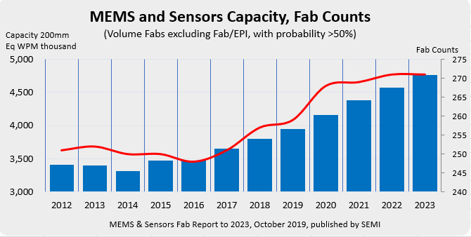
MILPITAS, Calif. — October 29, 2019 — Total worldwide installed capacity for MEMS and sensors fabs is forecast to grow 25 percent to 4.7 million wafers* per month from 2018 to 2023, driven by explosive demand across communications, transportation, medical, mobile, industrial and other Internet of Things (IoT) applications, according to the new MEMS & Sensors Fab Report to 2023 published by SEMI.

semi-logo

Listing more than 230 companies with over 400 facilities, the report is the first of its kind focused on MEMS and sensors front end facilities. The report, spanning the 12 years starting in 2012, predicts that MEMS fabs will account for 46 percent of all MEMS and sensors facilities by 2023. Image sensors fabs will represent 40 percent of the total, and other fabs – those producing both MEMS and image sensors – the remaining 14 percent.

Figure 1: Installed capacity and MEMS and sensors fab counts

Japan led the world in MEMS and sensors capacity in 2018, followed by Taiwan, the Americas, and Europe/Mideast. China is on track to rise from the sixth position this year to the third largest region in installed capacity by 2023. Japan and Taiwan are expected to maintain the top two positions through 2023.

The MEMS and Sensors Fab Report to 2023 shows fab equipment investments hovering at about US$4 billion per year from 2018 to 2023, with most of the spending – an estimated 70 percent – devoted to fabs for image sensors made on 300mm wafer sizes. During the same period, Japan’s fab equipment investment is expected to peak at nearly US$2 billion in 2020, with Taiwan topping out at US$1.6 billion in 2023.

All told, 14 new device volume fabs will be added from 2018 to 2023** for MEMS and sensors made on wafers ranging from 8 inches to 12 inches in size. China shows the largest increase in new volume fabs followed by Japan, Taiwan and Europe.

The MEMS & Sensors Fab Report to 2023 includes details on individual fabs such as location, technologies and products, as well as quarterly data from 2012 to 2023 for the following:

  • Construction and equipment investments
  • Installed capacities
  • Wafer sizes
  • Process nodes
MSIG Logo

SEMI Industry Research and Statistics developed the MEMS & Sensors Fab Report to 2023 in collaboration with the MEMS & Sensors Industry Group, a SEMI Strategic Association Partner. To learn more about the MEMS & Sensors Fab Report to 2023, click here.

*200mm equivalent capacity – excludes R&D, Pilot and EPI lines

**Excludes R&D, Pilot and EPI lines and fabs with low probabilities of being built
 

About SEMI

SEMI® connects more than 2,100 member companies and 1.3 million professionals worldwide to advance the technology and business of electronics design and manufacturing. SEMI members are responsible for the innovations in materials, design, equipment, software, devices, and services that enable smarter, faster, more powerful, and more affordable electronic products. Electronic System Design Alliance (ESD Alliance), FlexTech, the Fab Owners Alliance (FOA) and the MEMS & Sensors Industry Group (MSIG) are SEMI Strategic Association Partners, defined communities within SEMI focused on specific technologies. Visit www.semi.org to learn more, contact one of our worldwide offices, and connect with SEMI on LinkedIn and Twitter.

Association Contact

Michael Hall/SEMI
Phone: 1.408.943.7988
Email: [email protected]


Global and regional forces shaping the $2 trillion electronics industry have intensified more in the past few years than at any other time I can recall. The uncertainty bred by trade wars, corporate tax changes, new environmental regulations, immigration issues and STEM talent shortages is vexing the global microelectronics supply chain as companies shift investments and operational strategies to adjust to the unrelenting change and new realities with heightened urgency.In our industry, an increasingly dynamic world requires a more determined and strategic approach to advocacy. To meet the industry’s rapidly evolving needs, SEMI is transforming its global advocacy initiatives and programs. In the past 18 months, we have honed the focus of SEMI Global Advocacy to better serve member interests and needs, respond more quickly to fast-moving geopolitical developments, and deliver more value to help spur growth across the end-to-end electronics supply chain.Most importantly, SEMI Global Advocacy is now much more forward-looking and proactive. We have expanded our focus from primarily U.S. and independent regional issues to global affairs, allowing us to better leverage the power of our worldwide platforms. Organizationally, SEMI continues to add specialized staff advocates and calibrate its operational and member-driven engagement models to increase their involvement. There will be more to come, and with your continued support, we’ll be in a stronger position to meet your needs. Thank you!Strengthening the industry’s voiceThe rapid shift to a more proactive advocacy approach across all our initiatives was triggered by one disruptive action a little more than a year ago – the buildup and onset of the trade war between the United States and China. From the outset, SEMI formed strong member coalitions to intensify our lobbying efforts, met frequently with policymakers, submitted written comments to government panels, and issued public communications, all aimed at amplifying our collective voice. SEMI has taken a principled approach to advocacy, publicly stating its positions based on its trade pillars of free and fair trade/open markets, supply chain growth, respect for IP and national security.That approach was on full display as Japan tightened controls on exports to the Republic of Korea, sending shockwaves through the microelectronics industry. To minimize the industry impact, we leveraged our global reach and the counsel of our International Board of Directors to engage with both governments early on and ensure that Japan took into account our members’ interests in developing and implementing the new rules. In general, SEMI opposes the use of tariffs and limiting market access as levers to correct trade imbalances and other structural issues. Instead, we support dialogue and negotiations that lead to multilateral agreements aligned with our members’ interests and global trade principles.This year in the U.S. alone, SEMI advocates have met with more than 70 policymakers in Washington, D.C., including members of Congress and representatives from the White House, federal agencies and the Trade Representative’s office. We have also spoken with representatives from European and Asian government delegations. Since the trade war erupted, we have met with more than 220 policymakers worldwide, giving SEMI a seat at the table – a louder voice for our members – as we are increasingly seen as the voice of the end-to-end electronics manufacturing and design supply chain. SEMI Global Advocacy has also broadened its focus beyond public policy to address other areas of strategic importance to the industry such as the talent shortage.Expanding Advocacy’s global influenceSEMI’s public policy efforts now reach well beyond Washington, D.C. to all seven major manufacturing centers worldwide where we have regional offices, with SEMI advocacy staff in every location. This has created a network multiplier effect that allows us to rally our collective strength around common member interests. It’s no coincidence that our member-driven advocacy initiatives and programs have improved in parallel with expanded global participation by our member companies on our various policy and advocacy committees.Our Trade Advisory Committee, for example, has grown from 16 to 60 active members in the past year alone. This year, we have also formed working groups with SEMI members around the world to address talent pipeline challenges. The upshot is that we are now much more focused in attacking regional issues. Thank you once again.Despite changes in the strategic approach of SEMI Global Advocacy, we remain squarely focused on critical issues affecting industry growth and our members’ interests. In a nutshell, we call these the four T's: Tax – We strive to encourage rates that are fair to all companies, leveling the playing field globally Technology – We seek government investment in technology and innovation (R D) Trade – We advocate for open markets, free and fair trade as we promote our 10 Principles for the Global Semiconductor Supply Chain in Modern Trade Agreements worldwide Talent – We support education investments and immigration policies that provide opportunities and build the talent pipeline In addition, SEMI has long been a leading voice in promoting Environment, Health and Safety regulations that enable industry growth and demonstrate environmental stewardship – and we continue to make investments at this critical juncture as new technologies are driving changes in the regulatory landscape.Maintaining laser focus on member priorities amid shifting geopoliticsThe only way for SEMI Global Advocacy to navigate the cauldron of geopolitical disruption is to remain laser-focused on our members’ top priorities including trade, tax, technology and talent. And we will stick to what SEMI has done best for almost 50 years – facilitate public-private collaborations and more investment on behalf of our members.In workforce development, SEMI is taking bold steps to develop a robust talent pipeline, as much a growth and innovation driver for SEMI members and the industry as any technology. Announced earlier this year, SEMI Works™, our landmark talent development initiative, is already gaining steam with U.S. government investment and our rapid progress in laying its foundation with a database of standardized competencies for technical jobs as well as a certification and credentialing process for curriculum, education and training programs.The future for SEMI members and the industry is brimming with possibility. The strides SEMI Global Advocacy has made over the past year have only been possible through your support and involvement. As we broaden our scope beyond policy, we recognize that more progress needs to be made. We look forward to your continued participation as, together, we help our industry fulfill its great potential.Mike Russo is Vice President of Global Industry Advocacy at SEMI.
Read More

MILPITAS, Calif. — October 22, 2019 — North America-based manufacturers of semiconductor equipment posted $1.95 billion in billings worldwide in September 2019 (three-month average basis), according to the September Equipment Market Data Subscription (EMDS) Billings Report published today by SEMI. The billings figure is 2.4 percent lower than the final August 2019 level of $2.00 billion, and is 6.0 percent lower than the September 2018 billings level of $2.08 billion.

“Monthly billings of North American equipment manufacturers declined for the second consecutive month,” said Ajit Manocha, president and CEO of SEMI. “However, year-over-year billings shows signs of bottoming, and recent capital expenditure increases for leading-edge logic will provide near-term billings growth opportunities."

The SEMI Billings report uses three-month moving averages of worldwide billings for North American-based semiconductor equipment manufacturers. Billings figures are in millions of U.S. dollars.


Billings
(3-mo. avg.)

Year-Over-Year

April 2019

$1,922.0

-28.5%

May 2019

$2,065.2

-23.6%

June 2019

$2.026.1

-18.4%

July 2019

$2,031.9

-14.6%

August 2019 (final)

$2,001.8

-10.5%

September 2019 (prelim)

$1,953.7

-6.0%

Source: SEMI (www.semi.org), October 2019

SEMI publishes a monthly North American Billings report and issues the Worldwide Semiconductor Equipment Market Statistics (WWSEMS) report in collaboration with the Semiconductor Equipment Association of Japan (SEAJ). The WWSEMS report currently reports billings by 24 equipment segments and by seven end market regions. SEMI also has a long history of tracking semiconductor industry fab investments in detail on a company-by-company and fab-by-fab basis in its World Fab Forecast and SEMI FabView databases. These powerful tools provide access to spending forecasts, capacity ramp, technology transitions, and other information for over 1,000 fabs worldwide. For an overview of available SEMI market data, please visit www.semi.org/en/MarketInfo.

The data contained in this release were compiled by David Powell, Inc., an independent financial services firm, without audit, from data submitted directly by the participants. SEMI and David Powell, Inc. assume no responsibility for the accuracy of the underlying data.

About SEMI

SEMI® connects more than 2,100 member companies and 1.3 million professionals worldwide to advance the technology and business of electronics design and manufacturing. SEMI members are responsible for the innovations in materials, design, equipment, software, devices, and services that enable smarter, faster, more powerful, and more affordable electronic products. Electronic System Design Alliance (ESD Alliance), FlexTech, the Fab Owners Alliance (FOA) and the MEMS & Sensors Industry Group (MSIG) are SEMI Strategic Association Partners, defined communities within SEMI focused on specific technologies. Visit www.semi.org to learn more, contact one of our worldwide offices, and connect with SEMI on LinkedIn and Twitter.

Association Contact

Michael Hall/SEMI
Phone: 1.408.943.7988
Email: [email protected]

Notes

Next SEMI Billings report is November 19, 2019 at 3:00pm Pacific.

For information on SEAJ Book-to-Bill Report, visit www.seaj.or.jp

Artificial intelligence and machine learning are reshaping electronic system design as consumer-facing companies like Facebook and Google design their own hardware. Electronic system design is enabling rapid changes and new innovation in automotive. Designing microchips for the commercialization of outer space faces stiff challenges.These are just a few topics that companies driving technology innovation in electronic system design will discuss at SEMICON Europa, 12-15 November 2019 in Munich, Germany. In the run-up to the event, SEMI spoke with Bob Smith, executive director of the Electronic System Design (ESD) Alliance, a SEMI Strategic Association Partner, about how the integration of the ESD Alliance with SEMI’s global platforms is extending design expertise in the worldwide electronics industry. Smith shared his views ahead of the SMART Design Forum, 14 November 2019, 14:30 to 17:00, at SEMICON Europa. Registration is open. Join the forum to meet experts from ESD Alliance and other key industry influencers. Attendance is free of charge for all SEMICON Europa visitors (Hall B1, TechARENA 1).SEMI: In August of last year, SEMI announced the ESD (Electronic System Design) Alliance joined SEMI as a Strategic Association Partner. How does this partnership benefit the design and semiconductor industries?Smith: As indicated back then by Ajit Manocha, president and CEO of SEMI, “Design is the very foundation of semiconductor innovation and manufacturing.” The integration of the ESD Alliance with SEMI’s event and global platforms enables the design community to expand its expertise to the worldwide electronics industry. The integration helps streamline collaboration and connection of SEMI members with the electronic system design, IP and fabless communities.ESD Alliance members are now able to more efficiently engage with the electronics manufacturing supply chain on technical and business issues and gain access to comprehensive global resources and platforms. Those resources include SEMI’s technology communities and activities in areas such as advocacy, international standards and environment, health and safety (EH S), industry statistics, trade and regulatory initiatives.SEMI: And what were the main opportunities for the ESD Alliance to present the scope of the brand-new collaboration? How did the ESD Alliance enlarge the scope of the semiconductor and design industries?Smith: Although the ESD Alliance has international member companies, the reach and focus of our activities was limited to North America. SEMI’s global platform allows us to spread our design initiatives worldwide. In 2019 we introduced design at SEMICON events in China, Taiwan, the U.S. and now Europe with our participation in SEMICON Europa’s SMART Design Forum. By introducing design into these global events, we are advancing SEMI’s expanded mission to represent the entire global electronic design and manufacturing chain and tighten the connection between the semiconductor and design industries.Industrywide events like SEMICON Europa and its SMART Design Forum bring the entire electronic product supply chain closer together by focusing on commercial achievements in design and presenting forward-looking, system-centric views. The Smart Design Forum is a great opportunity for attendees to deepen their understanding of the links across design and manufacturing and throughout the supply chain during sessions and informal discussions at networking and social events. These exchanges help foster the collaborations essential to addressing technical challenges and ushering exciting new electronic products from concept to consumer.SEMI: How is the semiconductor design ecosystem evolving? What disciplines are becoming integrated with those that have historically governed the scene? Can you tell us more about the concept of system-centric view?Smith: In the early days of electronic design automation (EDA), design was largely separated from manufacturing. On the design side, the goal was to design and tape-out chips. After tape-out, the chip was handed off to the manufacturing group and the design team went on to a new project. We refer to this era as chip-centric.Now, given the complexity of both chips and electronic systems, design and manufacturing can no longer be separated. Instead, they must collaborate from the beginning of a project on all aspects of system design. This system-centric view enables the delivery of smarter, faster, more powerful, and more affordable electronic products. This is a big responsibility and meeting it demands tight cooperation and collaboration across multiple disciplines including semiconductor design, packaging, software development, materials and manufacturing, system integration and testing.SEMI: What’s one of your strategic objectives for 2020? Smith: In 2020 we plan to launch our Connecting the Divide initiative to bring the design and manufacturing communities closer together to help both better understand the role of the other, the value each provides and the unique challenges each community faces. The goal is to increase the rate of collaboration between design and manufacturing in answering both industries’ need for a system-centric approach to new electronic product/system design.SEMI: Do we have good reason to be optimistic about opportunities on the horizon? What’s one prediction for the future of semiconductor design solutions you’d like to share?Smith: We seem to be surrounded by almost limitless opportunities. In terms of design, my prediction is that we will see higher levels of system design abstraction that will allow systems to be rapidly configured and verified in a way that we cannot do today. In essence, we will be able to build virtual systems rapidly to reduce the risk and cost of developing new electronic products.SEMI: What are your expectations regarding the SMART Design Forum at SEMICON Europa 2019 in Munich? Smith: We are excited to be bringing the design conversation into SEMICON Europa at the SMART Design Forum. Europe has been recognized as a leading region in embracing and driving system design. Our objective is to move deeper into system-centric design through the exchange of information and ideas at the SMART Design Forum.Robert (Bob) Smith is Executive Director of the Electronic System Design (ESD) Alliance, a SEMI Strategic Association Partner. The ESD Alliance is an international trade association of companies providing goods and services throughout the semiconductor design ecosystem. Bob began his career as an analog design engineer at Hewlett-Packard working on disk drive technology. Since then, he has spent more than 30 years in various roles in executive management, marketing, and business development primarily working with startup and other early stage companies in Electronic Design Automation (EDA) and semiconductor IP. These companies include IKOS Systems, Synopsys, LogicVision, Magma Design Automation and Uniquify. He was a member of the IPO teams that took Synopsys public in 1992 and Magma public in 2001. Bob received his BSEE from U.C. Davis and his MSEE from Stanford University. Serena Brischetto is a marketing and communications manager at SEMI Europe.
Read More