downloadGroupGroupnoun_press release_995423_000000 copyGroupnoun_Feed_96767_000000Group 19noun_pictures_1817522_000000Member company iconResource item iconStore item iconGroup 19Group 19noun_Photo_2085192_000000 Copynoun_presentation_2096081_000000Group 19Group Copy 7noun_webinar_692730_000000Path
Skip to main content
Default Banner Image

SEMI News

Forum Connects Students, Young Professionals with Semiconductor Companies to Help Build Talent Pipeline

SWANSEA, United Kingdom – February 10, 2020 – Post-graduates and onboarding talent will connect with local companies to explore semiconductor industry career paths and employment opportunities at the SEMI Talent Forum , 6 March 2020 in Swansea, UK at the University of Swansea. Sponsored by SEMI , the industry association representing the global electronics manufacturing and design supply chain, and staged in partnership with European organizations including the University of Swansea , Edwards , Oxford Instruments , and SPTS Technologies , the event will also highlight how technology is reshaping the global workforce. Participation is free of charge and registration is open.

semi logo

The event will be held at the Great Hall, Swansea University Bay Campus, Fabian Way, Crymlyn Burrows, Swansea SA1 8EN, UK.

The SEMI Talent Forum is an ideal venue for semiconductor companies to promote their workforce development, diversity and inclusion initiatives to the next generation of industry talent. The forum targets young talent as the semiconductor industry presses ahead to build the workforce critical to innovations in cutting-edge technologies that are transforming how we work and live such as artificial intelligence (AI), Internet of Things (IoT), 5G, augmented/virtual reality (AR/VR), machine learning and quantum computing. Representatives from Swansea University and the Welsh Government will kick off the event with keynotes.

Talent forum logo

SEMI Talent Forum Key Topics

  • Technologies Addressing Global Challenges
  • Microelectronics Enabling AI, IoT and 5G
  • Technology Highlights from the CS Connected Cluster
  • Panel Discussion – Leading in the Digital Age: Technology, Diversity and Inclusion

Other Event Highlights

  • Tech Demo Zones – Interactive demonstrations of technologies such as VR
  • Career Café – Students and post-graduates will meet with industry leaders, learn about their companies’ work and culture, and participate in mock interviews and CV review sessions.
  • Professional Headshot Studio – Young talent will get a free professional headshot for their CV and business social media profiles.
  • Student Poster Exhibition – Local students will showcase their research.

For more details about the event, please see the full program .

The SEMI Talent Forum is sponsored by Edwards, Oxford Instruments and SPTS Technologies (A KLA Company).

Follow SEMI on Twitter and LinkedIn : @SEMIEurope – #talentforum #digitalfuture


About SEMI

SEMI® connects more than 2,100 member companies and 1.3 million professionals worldwide to advance the technology and business of electronics design and manufacturing. SEMI members are responsible for the innovations in materials, design, equipment, software, devices, and services that enable smarter, faster, more powerful, and more affordable electronic products. Electronic System Design Alliance (ESD Alliance), FlexTech, the Fab Owners Alliance (FOA) and the MEMS & Sensors Industry Group (MSIG) are SEMI Strategic Association Partners, defined communities within SEMI focused on specific technologies. Visit www.semi.org to learn more, contact one of our worldwide offices, and connect with SEMI on LinkedIn and Twitter .

Association Contact

Serena Brischetto
SEMI Europe
Email: [email protected]
Tel: +49 30 303080770
ww.semi.org/eu

MILPITAS, Calif. – February 4, 2020 – Worldwide silicon wafer area shipments in 2019 declined 7 percent from the 2018 record high while revenue remained above the $11 billion mark despite a global silicon revenue slip of 2 percent over the same period, the SEMI Silicon Manufacturers Group (SMG) reported in its year-end analysis of the silicon wafer industry.

semi logo

Silicon wafer area shipments in 2019 totaled 11,810 million square inches (MSI), while the industry logged shipments of 12,732 million square inches in 2018. Revenues in 2019 totaled $11.15 billion, edging down from the $11.38 billion posted in 2018.

“The 2019 decline in worldwide semiconductor silicon volume shipments resulted from memory market softness and inventory normalization,” said Neil Weaver, Vice President of SEMI SMG, and Director, Product Development and Applications Engineering, at Shin-Etsu Handotai America. “Despite the volume dip, silicon revenue remained resilient.”

Annual Silicon* Industry Trends


2008

2009

2010

2011

2012

2013

2014

2015

2016

2017

2018

2019

Area Shipments (MSI)


8,137

6,707

9,370

9,043

9,031

9,067

10,098

10,434

10,738

11,810

12,732

11,810

Revenues ($Billion)


11.4

6.7

9.7

9.9

8.7

7.5

7.6

7.2

7.2

8.7

11.4

11.2

Source: SEMI (www.semi.org), January 2020

*Total Electronic Grade Silicon Slices Excluding Non-Polished Wafers. Shipments are for semiconductor applications only and do not include solar applications.

*Shipments are for semiconductor applications only and do not include solar applications

All data cited in this release includes polished silicon wafers, such as virgin test wafers and epitaxial silicon wafers, as well as non-polished silicon wafers shipped to end users.

Silicon wafers are the fundamental building material for semiconductors, which, in turn, are vital components of virtually all electronics goods, including computers, telecommunications products, and consumer electronics. The highly engineered thin, round disks are produced in various diameters – from one inch to 12 inches – and serve as the substrate material on which most semiconductor devices, or chips, are fabricated.

The Silicon Manufacturing Group (SMG) is a sub-committee of the SEMI Electronic Materials Group (EMG) and is open to SEMI members involved in manufacturing polycrystalline silicon, monocrystalline silicon or silicon wafers such as cut, polished and epi. The group facilitates collective efforts on issues related to the silicon industry including the development of market information and statistics about the silicon industry and the semiconductor market.

For more information, please visit SEMI Worldwide Silicon Wafer Shipment Statistics.

About SEMI

SEMI® connects more than 2,100 member companies and 1.3 million professionals worldwide to advance the technology and business of electronics design and manufacturing. SEMI members are responsible for the innovations in materials, design, equipment, software, devices, and services that enable smarter, faster, more powerful, and more affordable electronic products. Electronic System Design Alliance (ESD Alliance), FlexTech, the Fab Owners Alliance (FOA) and the MEMS & Sensors Industry Group (MSIG) are SEMI Strategic Association Partners, defined communities within SEMI focused on specific technologies. Visit www.semi.org to learn more, contact one of our worldwide offices, and connect with SEMI on LinkedIn and Twitter.

Association Contact

Michael Hall/SEMI
Phone: 1.408.943.798
Email: [email protected]

MILPITAS, Calif. — February 3, 2020 — SEMI-FlexTech today announced the launch of six projects to accelerate sensor and sensor system innovations for new applications in industries including healthcare, automotive, industrial and defense. In collaboration with the U.S. Army Research Laboratory (ARL), FlexTech, a SEMI Strategic Association Partner, will provide more than $2.3 million in funding for the projects aimed at maturing the flexible-hybrid electronics (FHE) technology ecosystem. Organizations including the University of Texas El Paso, American Semiconductor, PARC, Tekscan, Alertgy and SAFI-Tech will lead the initiatives.

SEMI & FlexTech

“Flexible hybrid electronics give product designers new ways to use sensors to collect data and deliver actionable insights that improve how we work and live,” said Melissa Grupen-Shemansky, CTO of SEMI and Executive Director of SEMI-FlexTech. “This new round of projects epitomizes the wide range of applications enabled by innovations in flexible hybrid electronics. We expect this body of work to unearth new product roadmaps across the electronics industry.”

Projects


American Semiconductor, Inc., will develop 500 FHE ultra-thin, lightweight and configurable sensor systems with wireless capability for environmental sensing applications. ASI will partner with Boise State University, DuPont, HD Microsystems and ITN Energy Systems on the 15-month project.

American Semiconductor Logo

The University of Texas at El Paso will optimize structural and electrical performance and develop sculpted dielectrics for FHE 3D printing. The 12-month project will generate performance data and new algorithms for smarter 3D printing. A proof-of-concept, journal article and presentation will cap the project.

UTEP Logo

Tekscan will develop a functioning sensorized glove made of a durable resin with flexible-conductive and pressure-sensitive inks. The glove advances the state of the art for FHE pressure and force measurements and analysis, critical in design evaluation for automotive, consumer, packaging, robotics and medical devices. The 18-month project includes examinations of novel substrates and materials, hardware integration strategies, and manufacturing methods.


Tekscan Logo

PARC, A Xerox Company, will integrate a flexible and adaptable multi-sensor system (consisting of temperature, humidity, impact and gas sensors) with a single processor for data capture and both wireless and audio output capabilities. The system will target applications in the wearables, medical monitoring, Internet of Things (IoT), automotive and industrial markets. PARC will partner with Purdue University in this 12-month project.

PARC Logo

Alertgy will develop a curved, flexible and lightweight wrist-mounted FHE for non-invasive glucose monitoring. The wristband will incorporate electrical impedance spectroscopy (EIS), a transducer and a printed battery. The device interface will enable the integration of other sensors into its multipurpose design. A demonstration of the platform will culminate the 16-month project.

Alertgy Logo

will develop and demonstrate screen-printed, supercooled liquid metal particles for use in electrical interconnects at low temperatures as a replacement for electrically conductive adhesives (ECAs). Lower temperatures in electronics manufacturing can reduce heat generation, processing costs and thermal damage to components while enabling higher throughput for devices in defense, automotive, healthcare and other industries. SAFI-Tech will partner with Iowa State University on the18-month project.

SAFI Tech Logo

About SEMI

SEMI® connects more than 2,100 member companies and 1.3 million professionals worldwide to advance the technology and business of electronics design and manufacturing. SEMI members are responsible for the innovations in materials, design, equipment, software, devices, and services that enable smarter, faster, more powerful, and more affordable electronic products. Electronic System Design Alliance (ESD Alliance), FlexTech, the Fab Owners Alliance (FOA) and the MEMS & Sensors Industry Group (MSIG) are SEMI Strategic Association Partners, defined communities within SEMI focused on specific technologies. Visit www.semi.org to learn more, contact one of our worldwide offices, and connect with SEMI on LinkedIn and Twitter .

Association Contact

Michael Hall/SEMI
Phone: 1.408.943.7988
Email: [email protected]

The march of innovation in semiconductor microfabrication technology over the past 60 years has produced electronic devices and information systems that have transformed industries and lives around the world. And while advances in chip technology continue to make it possible to collect, transmit, store and process more data for a rapidly growing universe of applications, the pace of innovation is now facing strong headwinds. Powered by chip innovation, data centers have become massive centers of information processing but, on the downside, enormous consumers of electricity. Today, the power-hungry hubs account for five percent of the world's electricity usage, a proportion that is growing every year, raising important questions about sustainability. Compounding the challenge, the pace of Moore's Law, for decades the engine of electronic device and information system innovation, has slowed. While the research and development of state-of-the-art semiconductor fine processing technology remains robust, developing the advanced manufacturing technology for mass-producing more sophisticated electronics devices is becoming harder, as is ensuring business profitability."It has become difficult for semiconductor technology to continue to evolve as it has in the past," said Akira Minamikawa, Research Director of Technology Research at IHS Markit, who moderated the Semiconductor Executive Forum – View by Top Two in the Era of Digitalization on opening day of SEMICON Japan 2019 at Tokyo Big Sight. Held at the SuperTHEATER, the forum featured Terushi Shimizu, representative director and president at Sony Semiconductor Solutions, and Atsuyoshi Koike, president at Western Digital Japan, two industry powerhouses that could figure heavily in the future of digital technology. SuperTHEATER, the main stage at SEMICON Japan 2019 Image sensors evolve to become eyes of AIImage sensors are becoming eyes of artificial intelligence (AI) and intelligent systems that monitor people and events worldwide, collecting data that one day could help puzzle out growing social challenges such as energy conservation and traffic congestion. With 51 percent market share on the strength of its industry-leading technology, Sony Semiconductor Solutions dominates the image sensor market. Despite last year’s global semiconductor industry slump, the company’s “business continues to enjoy strong growth and we are very busy,” said Shimizu, who attributed the company’s robust performance to the rising importance of the social role of image sensors and the expanding number of applications they support.The success of the company’s image sensors can also be traced to its division of the image sensor market into two application categories: "Imaging" focuses on capturing beautiful image data, while "sensing" aims to collect data that accurately describes the state of a subject and its surroundings."In 2019, sales of imaging products for smartphones grew rapidly,” Shimizu said in his market overview. “This is due to the average annual 15 percent growth rate of multi-camera smartphones, with some phones today featuring seven cameras, and an average annual growth rate of 20 percent in sensor size to produce higher image quality."But Shimizu cautioned that Sony Semiconductor Solutions doesn’t expect the smartphone sensor market to maintain that fast growth rate."The imaging market is expected to grow until 2022, but after that, the sensing market will drive market growth,” he said, adding that the company’s “capital investment plan is based on this scenario."AI will be key in catalyzing growth of the sensor market as integrations of AI processing engines and sensing images grow in sophistication to capture images undetectable by the human eye, Shimizu said. AI will extract insight from captured image data. For its part, Sony will apply its layer stacking technology to sensing products."By stacking an AI processing engine, we want a significant portion of the recognition processing done within the sensor chip," Shimizu said.One sensor the company already offers collects in-depth information for indirect time-of-flight (ITOF) 3D ranging for new user interfaces relying on autonomous or gesture control for robotics. The sensor “was first used in smartphones in 2018 and saw widespread adoption in 2019," Shimizu said.Sony Semiconductor Solutions plans to focus on developing new sensors for integration with their ultrasonic cousins. Aided by optical deflection technology, the sensors will be used for product quality inspections during manufacturing.With the company’s growing strengths in sensor technology, it hopes “to increase sales of sensors from a few percent of the company’s total sales in 2018 to 30 percent in 2025,” Shimizu said, pointing to its goal "to capture 60 percent share of the image sensor market by 2025."Data as one way to spread happinessAt the heart of consumer devices such as smartphones and computers and also cloud servers, NAND flash has made it possible to process vast troves of data anytime, anywhere. In recent years, the technology has enjoyed stronger adoption for use as the storage medium of choice for edge computing, stationed between end devices and the cloud to help streamline data utilization. But the technology isn’t merely about making smarter use of bits and bytes."We would like to promote the technology development that can support the use of data to bring happiness to people around the world," Koike of Western Digital Japan said. The company calls data that contributes to individual happiness and helps solve social issues "data for good" and, like the Sony Semiconductor Solutions bifurcated classification of the image sensor market, categorizes information into “big data” and “fast data.”For example, big data can leverage AI to drive dramatic improvements in the interpretation of test data and, ultimately, the diagnostic accuracy of mammography for breast cancer screening, aiding in early detection to help save lives, Koike said. Fast data can be harnessed to analyze data collected from a manufacturing equipment line in real time to improve production efficiency. The company’s plant in Yokkaichi, Mie Prefecture, which the company operates in cooperation with Japanese memory manufacturer Kioxia, already uses fast data to bolster production.More NAND flash innovation and greater supply capacity are critical to developing "data for good," Koike said. "It is difficult to expand clean rooms at the same pace as data usage grows. In order to continue to advance technology and enhance supply capacity, we need to adopt new ideas for building production lines. We need a smaller equipment footprint, shorter cycle time and higher throughput."Semiconductor market shows signs of recoveryIn their discussion of the short-term outlook for the semiconductor market, Shimizu and Koike pointed to the importance of strengthening the talent pool of Japan’s semiconductor industry as global competition heats up with China’s pursuit of semiconductor independence and the industry pulls out of the 2019 slowdown fueled by weak memory prices. While Sony’s business has been buoyed by strong image sensor demand for smartphones, the devices “did very well, but other applications didn't," Shimizu said. Even the image sensor market stagnated.Despite the 2019 slump, market conditions and capital investments by semiconductor manufacturers have been on the upswing."In the second half of 2019, the Chinese market showed signs of recovery triggered by 5G,” Shimizu said. “In 2020, this movement is going to be in full swing around the world and we will be busier than last year."Koike agreed: "The semiconductor market for data centers will recover with 5G. The hard disk shortage is already an indication of a recovery, a turnaround that will undoubtedly extend to solid state drives (SSDs). In addition, advances in autonomous driving technology will ensure continued growth of the automotive semiconductor industry.”Japan should embrace international competition, not fear China's pursuit of chip independenceIt's no secret that China is investing heavily in its semiconductor development capabilities to move up the microprocessor value chain. Minamikawa posed the question: How should Japanese chip companies navigate the shifting regional balance of power? "It is natural for China to strive to establish domestic procurement of semiconductors that are fundamental technologies for various industries,” Koike said, “I think the efforts of Chinese companies are outstanding in that they are not pursuing short-term results, such as improving yields in the near future, but are making efforts with an eye to achieving results in 10 years. Japan has a variety of options including working with China to create joint ventures and competing head-on. Regardless of which choice we make, however, it is imperative for the survival of domestic companies that Japan maintains its technological competitiveness to remain ahead of China."Shimizu said that Sony’s “Chinese customers are quick to take action and study extremely hard. We often have opportunities to share our roadmap with them and explore innovation opportunities together. Before, they were passive and relied on us for insights into new technologies, but now they are more assertive and I sense that they will start to drive innovation.”Koike added that "although Japanese companies often talk about business globalization, neither Chinese nor American companies say much about it. While global expansion is a major requirement for business, I think Japanese companies need to focus more on the Japanese market overall, not just when they think about the growing competitiveness of Chinese companies." L-R: Akira Minamikawa, Research Director of Technology Research at IHS Markit; Atsuyoshi Koike, president at Western Digital Japan; Terushi Shimizu, representative director and president at Sony Semiconductor Solutions Talent key to bolstering competitiveness of Japan’s semiconductor industryMinamikawa of IHS Markit didn’t mince words in describing the talent shortage in the Japanese semiconductor industry as “grave,” saying that “the workforce challenge is not endemic to the electronics industry as evidence grows that the number of people obtaining doctorates in Japan is falling and the educational level of the Japanese population as a whole is in decline.”Three years ago, Shimizu interviewed professors on Kyushu island for insights into Japan’s talent shortfall. He came away feeling that “Japanese semiconductor companies were not sufficiently communicating the industry's talent and innovation needs to professors. To help professors and students better grasp the appeal and potential of the industry, we have started to send frontline engineers to universities to educate students and instructors about their work and careers. Expecting corporate HR departments to alone solve the talent shortage won’t work.”"In Japan, if you advance to a doctoral course, you will have a hard time getting a job, which is a strange situation,” Koike said. “Companies and universities need to work together more closely to better understand how to attract and hire doctoral graduates."Minamikawa said companies must have strong leaders with clear missions to attract the right talent, but Koike pointed to the drawbacks: "The image of a company with a strong leader seems to be cool, but it also has a downside because engineers stop thinking for themselves and wait for instructions from the top. I believe it is important for company leaders to have ongoing discussions at all organizational levels and lead the way in times of confusion."Shimizu agreed, citing his own company as an example."Thankfully, our company is very busy right now,” he said. “However, some employees are starting to request more time to think about how to improve the quality of their work. To maintain and strengthen our competitiveness and continue business growth, I believe it is important to cultivate an environment that encourages each employee to take more time to think for themselves."Motoaki Ito is the CEO of Enlight, Inc. and a reporter for SEMI. Mayumi Amagai is a marketing manager at SEMI Japan.
Read More

DRESDEN, Germany — 27 January, 2020 — The SEMI 3D & Systems Summit opens today in Dresden, Germany, with top experts in 3D integration and systems for semiconductor manufacturing applications providing the year’s first comprehensive outlook for advanced packaging and systems. Themed Expanding Application Space, the annual three-day summit features the latest developments and insights in artificial intelligence (AI), 5G, heterogeneous integration, 3D roadmap and System-In-Package (SiP) technologies.

3D Systems Summit Logo

With automotive expected to rank among the strongest growth markets for semiconductors and advanced packaging in the coming decades, opening keynote speaker, Jan Vardaman, president and founder of TechSearch International Inc., will highlight packaging types essential for AI chips in automotive. Vardaman will also explore AI’s vital role in emerging healthcare, mobile, fintech and smart home technologies.

“The SEMI 3D & Systems Summit highlights Europe’s prowess in developing the advanced packaging and manufacturing systems key to the rapid adoption of 5G, AI, AR/VR, quantum computing and other leading-edge technologies,” said Laith Altimime, president, SEMI Europe. “The ‘20s promise astonishing innovations as the semiconductor industry drives to make a smarter world a reality.”

According to a recent Yole Développement report, advanced packaging has entered an era of great promise fueled by the critical need for improvements in chip component integration in order for 5G, AI, IoT, Industrial Internet of Things (IIoT), and high-performance computing (HPC) to flourish. Emilie Jolivet, Semiconductor and Software Division Director at Yole Développement, will discuss how heterogeneous integration will enable new HPC applications.

With wafer-level packaging (WLP), 3D stacking and SiP key to meeting the stringent form factor, high-speed and power consumption requirements for mobile devices, Romain Freux, CEO of System Plus Consulting, will explore the latest advanced packaging trends for mobile computing.

The 3D & Systems Summit offers business-to-business matchmaking, networking for participants to explore new partnerships, an exhibition, and a gala dinner. Visit 3D & Systems Summit for more information.

Follow #3DSummit @SEMIEurope on LinkedIn and Twitter.

About SEMI

SEMI® connects more than 2,100 member companies and 1.3 million professionals worldwide to advance the technology and business of electronics design and manufacturing. SEMI members are responsible for the innovations in materials, design, equipment, software, devices, and services that enable smarter, faster, more powerful, and more affordable electronic products. Electronic System Design Alliance (ESD Alliance), FlexTech, the Fab Owners Alliance (FOA) and the MEMS & Sensors Industry Group (MSIG) are SEMI Strategic Association Partners, defined communities within SEMI focused on specific technologies. Visit www.semi.org to learn more, contact one of our worldwide offices, and connect with SEMI on LinkedIn and Twitter.

Association Contact

Serena Brischetto / SEMI Europe
Phone: +49 30 3030 8077-11
Email: [email protected]

MILPITAS, Calif. — January 23, 2020 — North America-based manufacturers of semiconductor equipment posted $2.49 billion in billings worldwide in December 2019 (three-month average basis), according to the December Equipment Market Data Subscription (EMDS) Billings Report published today by SEMI. The billings figure is 17.5 percent higher than the final November 2019 level of $2.12 billion, and is 18.4 percent higher than the December 2018 billings level of $2.10 billion.

SEMI

“Monthly billings of North American equipment manufacturers reached a level not seen since June 2018,“ said Ajit Manocha, president and CEO of SEMI. “The December surge in equipment billings reaffirms the strength of leading-edge logic and foundry investments.”

The SEMI Billings report uses three-month moving averages of worldwide billings for North American-based semiconductor equipment manufacturers. Billings figures are in millions of U.S. dollars.


Billings
(3-mo. avg.)

Year-Over-Year

July 2019

$2,031.9

-14.6%

August 2019

$2,001.8

-10.5%

September 2019

$1,959.1

-5.7%

October 2019

$2,080.8

2.5%

November 2019 (final)

$2,121.0

9.1%

December 2019 (prelim)

$2,491.7

18.4%

Source: SEMI (www.semi.org), January 2020

SEMI publishes a monthly North American Billings report and issues the Worldwide Semiconductor Equipment Market Statistics (WWSEMS) report in collaboration with the Semiconductor Equipment Association of Japan (SEAJ). The WWSEMS report currently reports billings by 24 equipment segments and by seven end market regions. SEMI also has a long history of tracking semiconductor industry fab investments in detail on a company-by-company and fab-by-fab basis in its World Fab Forecast and SEMI FabView databases. These powerful tools provide access to spending forecasts, capacity ramp, technology transitions, and other information for over 1,000 fabs worldwide. For an overview of available SEMI market data, please visit www.semi.org/en/MarketInfo.

The data contained in this release were compiled by David Powell, Inc., an independent financial services firm, without audit, from data submitted directly by the participants. SEMI and David Powell, Inc. assume no responsibility for the accuracy of the underlying data.

About SEMI

SEMI® connects more than 2,100 member companies and 1.3 million professionals worldwide to advance the technology and business of electronics design and manufacturing. SEMI members are responsible for the innovations in materials, design, equipment, software, devices, and services that enable smarter, faster, more powerful, and more affordable electronic products. Electronic System Design Alliance (ESD Alliance), FlexTech, the Fab Owners Alliance (FOA) and the MEMS & Sensors Industry Group (MSIG) are SEMI Strategic Association Partners, defined communities within SEMI focused on specific technologies. Visit www.semi.org to learn more, contact one of our worldwide offices, and connect with SEMI on LinkedIn and Twitter.

Association Contact

Michael Hall/SEMI
Phone: 1.408.943.7988
Email: [email protected]

Notes

Next SEMI Billings report is February 20, 2020 at 3:00pm Pacific.

For information on SEAJ Billings Express Report, visit www.seaj.or.jp.

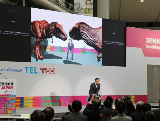
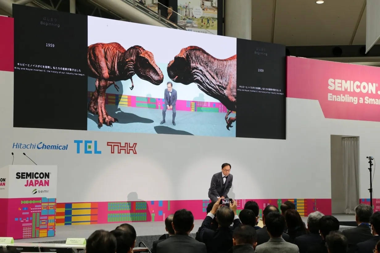
Augmented reality (AR) tyrannosauruses towered on-screen as I interacted with the creatures in a mix of prehistoric and cutting edge. Or, rather, my AR double was doing the playacting. Minutes later, virtual doppelgangers of a small lineup of chip industry executives cut the ceremonial ribbon. Seemingly sweeping away the winter chill, the opening of SEMICON Japan 2019 dazzled with smart technology and the promise of lives, cities and workplaces transformed, with uber-intelligent applications in full display at Tokyo Big Sight. But what resources does the industry need to harness to drive the next era of innovation? The semiconductor industry’s unwavering passion and young talent are key, said Hiroshi Imano, Chairperson of the SEMICON Japan Initiatives Committee, in his opening keynote. And hardly any region of the world is in a better position to help realize that future than Japan, Imano said. The region supplies one third of the equipment and more than half of all materials to the global semiconductor manufacturing industry.Talent was also top of mind for SEMICON Japan 2019 keynote speaker Makiko Eda, Japan's Chief Representative Officer at the World Economic Forum (WEF). Serving as a platform for public-private partnerships, the organization's mandate is to tackle global issues such as climate change and geopolitical strife in making world more resilient to risk and, by extension, more sustainable.Spanning ecology, economy, technology, society, geopolitics and industry, that mission includes reskilling and upskilling a billion people over the next decade, a high priority for WEF, which hosts a conference every January in Davos, Switzerland. The theme of this month's conference – Stakeholders for a Cohesive and Sustainable World – reflects the vital importance of building the international partnerships and global consensus necessary to achieving WEF's goals.One key to that sustainability will be technology and Arm, a global chip design company, will play a key role, with the company’s chips touching over 70 percent of the world’s population, Arm president Yuzuru Utsumi said in his keynote. Today, Arm is driving toward an ambitious goal: Ship 100 billion chips from 2017 to 2021 – the same number produced over the previous quarter century – by powering advances in mobile computing, server and networking infrastructures, and automotive applications.Arm’s innovation ecosystem of more than 1,000 partners will deliver these chips as they continue to work together to develop differentiated technology. Arm plans to increase investments not only in its primary processor business to accelerate market share gains but in the company’s new IoT business to create new revenue streams. The goal: Deliver long-term sustainable growth, Utsumi said. SEMICON Japan 2019 showcases SMART manufacturing and transportation Billed as a showcase of smart technologies, SEMICON Japan 2019 delivered with an array of eye-grabbing exhibitions in the popular SMART Applications Zone. In the SMART Transportation area, the automatic operation pavilion featured a car equipped with open-source software for autonomous driving. The exhibitor, Tier IV, aims to help lead the early commercialization of self-driving vehicles through the adoption of its software, Autoware, which makes it easier to develop self-driving vehicle prototypes using low-power platforms.Sony Semiconductor Solutions demonstrated a vision sensing processor designed to guide autonomous drones. Using two cameras, the processor measured the changing distance between visitors moving about the exhibit and stationary objects in real time, indicating proximity in hues of red (nearby) and blue (at a distance). Many visitors were wowed, describing the multichromatic display as futuristic.Others rode a simple wooden swing hanging by two ropes, but from dizzying heights thanks to Solidray’s Duo-Sight, a virtual reality (VR) system that projects 3D images stretching from wall to floor for immersive experiences. One visitor thrilled at how riding the swing, suspended only a few feet from the floor, felt like soaring on a flying trapeze. Target applications for the technology include virtual rides at amusement parks and presenting interior design options to homeowners.In the SMART Manufacturing area, one highlight was the demonstration by the National Institute of Advanced Industrial Science and Technology (AIST) of a remote-controlled Minimal Fab System designed for low-volume, high-mix chip production with little staffing. Designed to increase production efficiency, the system allows a circuit designer to manufacture a semiconductor by singlehandedly operating equipment up and down the production line. Controlling nearly 50 pieces of equipment, the Minimal Fab System on display manufactured chips that were verified for functional operation and exhibited afterwards.On the SMART Applications stage, exhibitors DENSO and Toyota Motor Corporation announced a new joint venture to conduct research and advanced development of the next-generation in-vehicle semiconductors critical to electric and autonomous vehicle innovation. The venture, operating as MIRISE Technologies, will combine Toyota’s mobility expertise with DENSO’s in-vehicle component prowess. The goal is to build a rapid, competitive development system by 2030, said Yoshifumi Kato, executive director of the DENSO Research and Development Center, and president and representative director of the venture. On track to begin work this year, MIRISE will span three fields of technology development: power electronics, sensing and SoC (System-on-a-Chip). The name MIRISE combines word the Japanese word "mirai" (future) with "rise."Business Continuity PlanningNatural disasters and other emergencies are an ongoing threat to uninterrupted business operations across the semiconductor manufacturing supply chain and particularly in earthquake-prone Japan. To better prepare for business disruptions and restore normal operations as soon as possible after disaster strikes, more companies are teaming on Business Continuity Planning (BCP).THK's Seismic Isolation Experience Car demonstrated one technology designed to help – a seismic isolation device. The car shakes like an earthquake to give people inside a taste of how a building heaves and sways during a quake with and without the device deployed. Visitors were struck by how much the isolator dampens tremors to prevent or minimize damage. In the BCP seminar, representatives from Sony Semiconductor Manufacturing, THK, DISCO and Team Engineering Consulting shared lessons learned from actual disasters and discussed the critical importance of daily disaster drills. Yukihide Keigo, Executive Engineer in charge of Products and Development at Sony Semiconductor Manufacturing, recounted how the company’s Kumamoto Prefecture plant struggled for 96 days to restore full operations after the facility sustained heavy damage in the 2016 earthquake. Keigo said the plant lacked the structural reinforcements necessary to withstand the impact and fell prey to poor planning and accountability. The Kumamoto plant has since implemented measures – structural and procedural improvements – that more accurately account for seismic risks to ensure full recovery within 56 days. The plant’s new procedures include emergency drills for staff including night-shift workers.Innovation abounds at six SuperTHEATER forumsSEMICON Japan 2019 was held in the West and South Halls of Tokyo Big Sight as organizers of the Tokyo Olympics occupied the East Hall, the exhibition's usual home at the venue, to prepare for the 2020 games. For the first time, the main stage, SuperTHEATER, was set up in the cavernous arena near the main entrance. The SuperTHEATER featured six forums over three days. Semiconductor Executive Forum – View by Top Two in the Era of Digitalization with thought leaders from IHS Markit and Sony Semiconductor Solutions SMART Connectivity Forum – Infinite World Brought by 5G Innovation with experts from Softbank and Nokia Solutions Networks SMART Transportation Forum I – Front-line of Automated Driving featuring speakers from Intel and DENSO SMART Transportation Forum II – Revolution of Sky Transportation, supported by the U.S. Commercial Service in Japan, with presenters from Ministry of Economy, Trade and Industry (METI), Subaru and Bell Helicopter Manufacturing Innovation Summit – Issues and Innovation: What will Drive Growth to 2030 featuring thought leaders from VLSI Research, Applied Materials, KLA, Nikon and Tokyo Electron Mirai Vision Forum – Future Relation of Technology and Body 2.0 with speakers from Leave a Nest, Ory Lab and Autonomous Control Systems Laboratory The Mirai Vision Forum highlighted advanced technologies that could lead to societal improvements. One presenter, Kentaro Yoshifuji, CEO at Ory Lab, recalled how, as a child, he once stayed home from school while recovering from an illness. His imagination in full flight, the youngster imagined having a clone that could attend school and be with his classmates. The experience eventually inspired him to develop OriHime, a robot that gives socially isolated people a way to communicate with friends or colleagues remotely. Originally developed for physically impaired people, OriHime today is used to help the able-bodied. The robot is situated with the companion and the user operates OriHime remotely. A camera and monitor in OriHime’s face provide the visual and audio connection and the user controls the device with a smartphone or tablet or, for those who are paralyzed, through eye movement. One potential application: With OriHime stationed at a business office, working mothers could use OriHime to telecommute to better balance their careers with their parenting responsibilities at home. The robot would be a mother’s go-between, enabling her to communicate directly with colleagues.The next generation of innovators also took the stage as five teams presented innovative business ideas in friendly competition. The top prize in The TECH CAMP Hackathon went to the group that hatched an ingenious plan to develop a jacket that trains users to move their bodies in preprogrammed ways. For example, legendary Japanese professional baseball player Shigeo Nagashima could wear the gear while batting to program the device, then give the jacket to someone who’s never swung a baseball bat. The jacket would help the user replicate Nagashima’s swing. Now comes the real work of any innovator – executing on the vision.And then came two soccer-playing artificial intelligence (AI) robots that squared off and ... Scored! The demonstration by the Toyota National College of Technology started as a research project by Toyota National College students in 2002. The young innovators designed and developed all the robotic hardware and software from scratch. Looking ahead to SEMICON Japan 2020!SEMICON Japan 2019 not only gathered leading Japanese semiconductor materials and manufacturing equipment providers to demonstrate their latest innovations. The premiere regional event also provided insights on key trends critical to the entire electronics manufacturing supply chain. This year’s event drew more than 51,000 visitors and 695 exhibitors from 15 regions filling more than 1,700 booths.SEMICON Japan 2020 returns to East Hall at Tokyo Big Sight in December 2020. I look forward to seeing you there!Jim Hamajima is president of SEMI Japan.
Read More

HALF MOON BAY, Calif. – January 14, 2020 – The SEMI Industry Strategy Symposium (ISS) opened yesterday with the theme Data Driven Innovation and Growth. The annual three-day conference of C-level executives gives the year’s first comprehensive outlook of the global electronics manufacturing industry.

ISS Icon

For the nearly 300 attendees at ISS 2020, opening day highlighted market and technology opportunities and a reflection on the significant pricing and international trade challenges the semiconductor manufacturing supply chain faced in 2019. Deep discussions on technology disruptions, the future of mobility and 5G, and perspectives on the semiconductor industry in Asia will mark today, Day 2. Day 3 will feature presentations on advanced computing’s impact on the semiconductor industry and convene an expert panel titled Stock Wars: The Rise of SemiCaps to culminate the annual SEMI kick-off event for business leaders.

Opening keynote speaker Richard Gottscho, Executive Vice President and Chief Technology Officer at Lam Research, sees computational advances as one key to the semiconductor industry evolving from a little data world, marked by engineering teams taking several months to solve wafer etching problems, to one where big data is used to quickly and efficiently address issues. With etch recipes for wafers growing far more complex, the semiconductor industry needs a breakthrough in metrology technology to continue its virtuous cycle of positive, exponential feedback that has led to the increasingly faster pace of technology evolution. Gottscho compared data gathering by wearables to make general predictions on health to the potential use of metrology tools in collecting wafer data to predict fab health and avoid unscheduled downtime. Cost and time constraints still challenge the industry, yet Gottscho is optimistic that computational advances have brought the big metrology problem in a little data world close to resolution.

In the Economic Trends session, presenters took on macroeconomic trends and detailed industry-specific forecasts.

Daniel Niles, AlphaOne Capital, expects the semiconductor industry to resume growth in 2020 after five to six difficult quarters as semiconductor pricing stabilizes. However, he urged cautioned amid signs of economic risk, particularly how central banks worldwide are taking on debt, and a possible election-year surprise in the U.S. Industry tailwinds include an anticipated uptick in data center capital expenditures, improving inventory levels, progress in U.S.-Sino trade relations despite slow economic growth in China, and bullish secular trends in 5G, AI, IoT, AR, cloud, electric vehicles, autonomous driving and smart homes.

Michael Schallehn, Bain & Company, noted that the era of plentiful labor is nearing an end, posing a major challenge for economies worldwide as companies struggle to fill open positions. Robotics and automation could fill the employment gap to sustain economic growth as the cost of robotics falls and adoption of AI for customer service applications continues to rise. Workforce shortages offer a compelling business case for replacing human workers with robots, which can cut labor costs by 10 percent to 15 percent while boosting productivity as much as 30 percent. Over the next 10 to 20 years, Schallehn expects 20 percent to 25 percent of the global labor force to be displaced by robots, another significant challenge.

Kevin Anderson, IHS Markit, observed that the 2020 semiconductor revenue rebound will be led by memory, with growth exceeding 10 percent. Among 2020 industry growth drivers, 5G is the most promising, though its rollout will be phased. With development slower than forecast, autonomous driving will start to fulfill its promise after 2025. Mainstream AI applications were few in 2019 and the technology will only make a meaningful contribution to chip industry revenue once high-volume applications emerge. In its forecast for 2020, IHS Markit sees 5.5 percent annual growth for the global semiconductor industry with memory expanding at a 3.9 percent rate.

Bob Johnson, Gartner, pointed to TSMC’s outsize influence in the Gartner forecast for 5 percent CAGR in foundry revenue through 2023. Advanced nodes and rising demand for 5G 7nm chips will drive an increase in foundry capital expenditures over this period. In the equipment market, CapEx was down 6.9 percent year-over-year (YOY) in 2019 and is expected to improve slightly in 2020 with a 3.6 percent YOY decline. Johnson reported that more than 220 million 5G smartphones are expected to ship this year, but cautioned that the technology is at the peak of its hype cycle. Commercial applications are not yet available, most 5G phones will be using expanded 4G networks, and 5G usage in Korea recently underwhelmed – all signs that 5G is not ready for robust adoption, though the technology’s future is bright.

John West, VLSI Research Europe, highlighted the challenge to semiconductor equipment companies of navigating 5 percent CAGR in critical subsystem and component costs. Equipment makers must reduce costs without increasing risk. Their options include squeezing the profit margins of critical subsystem suppliers and turning to new models such as renting equipment, but he encouraged the manufacturers to analyze the segment before cutting costs. Pointing to a need for a risk heat map for the supply chain, West advised equipment manufacturers to consider several factors in evaluating critical subsystem supplier risk such as location given potential geopolitical instability, ability to deliver, financial strength, and current versus planned production capacity.

The afternoon session focused on Market Perspectives, on topics including intelligent surgery, biomedical 3D printing, and technology innovation.

Shawn DuBravac, Avrio Institute, highlighting CES 2020 product introductions, discussed how AI is driving down the cost of predictive applications and, along with cameras and sensors, has spawned a broad range of innovations. Examples include autonomous positioning and temperature regulation for beds to keep people asleep longer and reduce snoring, refrigerators that select recipe options based on available food, digital exoskeletons that make users 20 times stronger, self-driving wheelchairs, and robots for last-mile deliveries. He also pointed to a new age of virtual reality immersion that includes devices such as suits that provide tactile feedback to help train outdoor workers to perform tasks in a virtual weather environment of wind and rain.

Jonathan Sorger, Intuitive Surgical, focused on the many benefits of robotic surgical tools that follow a surgeon’s movements to extend innately human capabilities, reduce variability in surgical skills, help surgeons refine their skills through simulation, and provide surgeons with performance data for other improvements. For patients, robotic devices decrease wound infection and blood loss while requiring fewer incisions and open surgeries, accelerating recovery.

Severine Valdant Zygmont, Oxford Performance Materials, noted how data-driven processes have improved medical applications. One example is 3D printing of bone reconstructions using PEKK polymers to enable bone implants that are better personalized for patients. Concerns include how the medical industry will manage the newfound wealth of available data while protecting patient information.

Bradley Horowitz, Google, explored how companies can remain innovative as they grow, age and become susceptible because of complacency to rapid, disruptive innovation that can threaten their businesses. He highlighted four pillars of Jeff Bezos’ business philosophy: stay focused on customers, concentrate on results not process, look outside the company, and make decisions quickly. He also pointed to Google’s work as a startup incubator to enable innovation not otherwise possible and keys to success including mentorship, access to capital, and a sense of community.

Days 2 and 3 at ISS will delve deeper into the industry with presentations by Western Digital, ASML, JCET Group, Ford Motor Company, Bosch, Lyft, ASE, Qualcomm, Qorvo, Ericsson, International Business Strategies (IBS), Stratfor, Cabot Microelectronics, Arm, Entegris, Intel and Headgate Partners.

The SEMI Industry Strategy Symposium (ISS) examines global economic, technology, market, business and geo-political developments influencing the global electronics manufacturing industry along with their implications for your strategic business decisions. For more than 35 years, ISS has been the premier semiconductor conference for senior executives to acquire the latest trend data, technology highlights and industry perspective to support business decisions, customer strategies and the pursuit of greater profitability.

About SEMI

SEMI® connects more than 2,100 member companies and 1.3 million professionals worldwide to advance the technology and business of electronics design and manufacturing. SEMI members are responsible for the innovations in materials, design, equipment, software, devices, and services that enable smarter, faster, more powerful, and more affordable electronic products. Electronic System Design Alliance (ESD Alliance), FlexTech, the Fab Owners Alliance (FOA) and the MEMS & Sensors Industry Group (MSIG) are SEMI Strategic Association Partners, defined communities within SEMI focused on specific technologies. Visit www.semi.org to learn more, contact one of our worldwide offices, and connect with SEMI on LinkedIn and Twitter.


Association Contact

Michael Hall/SEMI
Email: [email protected]
Phone: 1.408.943.798

DRESDEN, Germany – 14 January, 2020 – Top experts in 3D integration and systems for semiconductor manufacturing applications will gather at the SEMI 3D & Systems Summit, 27-29 January, 2020, in Dresden, Germany, for the latest developments and insights in 5G, High-Performance Computing (HPC), Heterogeneous Integration, 3D Roadmap and System-In-Package technologies. Global thought leaders from ASE Group, Huawei Technologies, TSMC and TechSearch International will headline the event with keynotes. Event registration is open.

The 3D & Systems Summit will showcase prominent players in 3D integration for microelectronics manufacturing while offering business-to-business matchmaking, networking for participants to explore new partnerships, an exhibition, and a gala dinner.

SEMI 3D & Systems Summit Keynotes

Jan Vardaman
Jan Vardaman President and Founder, TechSearch International Inc.
TechSearch Logo
Vardaman will kick off the summit with her keynote A New Era for 3D. Vardaman will discuss the latest developments and trends in areas including three-layer image sensors, Samsung’s three-layer stack, new packaging technologies with active interposers, Foveros 3D integration technology for heterogeneous system integration, 3D and SoIC face-to-face stacking, Wafer-on-wafer (WoW) and High Bandwidth Memory (HBM).
Eelco Bergman photo
Eelco Bergmann Senior Director, Strategic Sales and Business Development, ASE Group
ase group logo
Leading day two with his keynote Integration Technologies Transforming the World, Bergmann will explore how System-in-Package (SiP) technologies are delivering on their promise of miniaturization, power efficiency and high performance. The timing of his keynote is ripe as the electronics industry, largely driven by semiconductor innovation, is enabling life-changing applications from health to mobility and from virtual reality to AI.
Dr. Douglas Yu
Dr. Doug Yu Vice President of Integrated Interconnect and Packaging, TSMC
TSMC Logo
In his presentation SoIC - A Longtime Game Changer, Yu will present research and development of advanced packaging and system integration solutions, System on Integrated Chips (SoICTM) and their derivatives, TSMC’s wafer-level system integration technologies, Chip on Wafer on Substrate (CoWoS®), and Integrated Fan-Out (InFO).
Mustafa Badaroglu
Mustafa Badaroglu Technical Director, Huawei Technologies
Huawei
In his talk 3D IC Opportunities for High-performance Computing, Badaroglu will explore trends in intelligent data connectivity, HPC, how sensors are driving energy-efficiency for computing, connectivity bandwidth, and new assembly and integration schemes such as 3D integration for energy-efficient machine learning computation.

Visit 3D & Systems Summit for more information. Follow #3DSummit @SEMIEurope on LinkedIn and Twitter.     

About SEMI

SEMI® connects more than 2,100 member companies and 1.3 million professionals worldwide to advance the technology and business of electronics design and manufacturing. SEMI members are responsible for the innovations in materials, design, equipment, software, devices, and services that enable smarter, faster, more powerful, and more affordable electronic products. Electronic System Design Alliance (ESD Alliance), FlexTech, the Fab Owners Alliance (FOA) and the MEMS & Sensors Industry Group (MSIG) are SEMI Strategic Association Partners, defined communities within SEMI focused on specific technologies. Visit www.semi.org to learn more, contact one of our worldwide offices, and connect with SEMI on LinkedIn and Twitter. 

Association Contact

Serena Brischetto
SEMI Europe
Email: [email protected]
Phone: +49 30 3030 8077-11
 

SEOUL, South Korea – January 14, 2020 – Semiconductor industry innovators SK hynix, Intel, imec and Graphcore will kick off SEMICON Korea 2020 with keynotes focusing on the future of artificial intelligence (AI) as an estimated 500 companies and 55,000 visitors gather February 5-7 at the COEX in Seoul for the latest microelectronics developments, innovations and trends powering the next wave of industry growth.

Themed Design the Smarter Future, SEMICON Korea 2020 will feature more than 30 technology programs offering leading insights into semiconductor manufacturing, AI, MEMS and sensors, mobility, and metrology and inspection. The event also includes a 2020 market outlook and a workforce development program to educate university students about career opportunities in semiconductor manufacturing as the industry works to fill its skills gap.

SEMICON KOREA 2020 Keynote Speakers

Jinkook Jim Photo
Jinkook Kim Executive Vice President, SK hynix
SK Hynix Logo
Information and communications technologies (ICT) are enabling a smarter world that is spawning vast amounts of data requiring advanced memory. In his presentation Semiconductor Technology for the Future ICT World, Kim will discuss how SK hynix is developing solutions to meet computing’s growing demand for low-power, high-capacity, high-speed memory to process this data.  
Mike Davies Photo
Mike Davies Director, Neuromorphic Computing Lab, Intel
Intel Logo
Delivering faster speeds and lower power than traditional semiconductors, neuromorphic chips are key for on-device AI data processing. With Intel transforming into a data-driven company with a keener focus on technologies such as AI, Davies will explore Neuromorphic Computing for Future Breakthroughs in AI while revealing more about Intel's shift in strategic direction.
Jan M Rabaey Photo
Jan M. Rabaey CTO of the System-Technology
Co-Optimization (STCO) Division, imec
imec logo
While the bulk of the interest and investment in AI has centered on cloud AI, excitement is growing around the promise of edge computing. Rabaey of imec, the world's largest semiconductor research institute, will discuss success pathways for edge computing and recommend ways to fulfill its potential in his presentation The Cognitive Edge.
Nigel Toon photo
Nigel Toon CEO and Co-founder, Graphcore
Grapmcore Logo
The amount of compute required to train complex AI models has grown by 300,000x since 2012. Compute gains have been a key component of AI progress and the industry is now preparing for the implications of systems far outside today’s capabilities. Toon will identify drivers of the huge appetite for more AI compute and describe how Graphcore’s IPU technology scales to meet this demand.

Admission to the keynote speeches is complimentary with event pre-registration by Wednesday, January 29, 2020. The keynotes will be held at the COEX Auditorium in Seoul.

About SEMI

SEMI® connects more than 2,100 member companies and 1.3 million professionals worldwide to advance the technology and business of electronics design and manufacturing. SEMI members are responsible for the innovations in materials, design, equipment, software, devices, and services that enable smarter, faster, more powerful, and more affordable electronic products. Electronic System Design Alliance (ESD Alliance), FlexTech, the Fab Owners Alliance (FOA) and the MEMS & Sensors Industry Group (MSIG) are SEMI Strategic Association Partners, defined communities within SEMI focused on specific technologies. Visit www.semi.org to learn more, contact one of our worldwide offices, and connect with SEMI on LinkedIn and Twitter.

Association Contact

Jaegwan Shim
SEMI Korea
Email: [email protected]
Phone: 82.2.531.7804