downloadGroupGroupnoun_press release_995423_000000 copyGroupnoun_Feed_96767_000000Group 19noun_pictures_1817522_000000Member company iconResource item iconStore item iconGroup 19Group 19noun_Photo_2085192_000000 Copynoun_presentation_2096081_000000Group 19Group Copy 7noun_webinar_692730_000000Path
Skip to main content
Default Banner Image

SEMI News

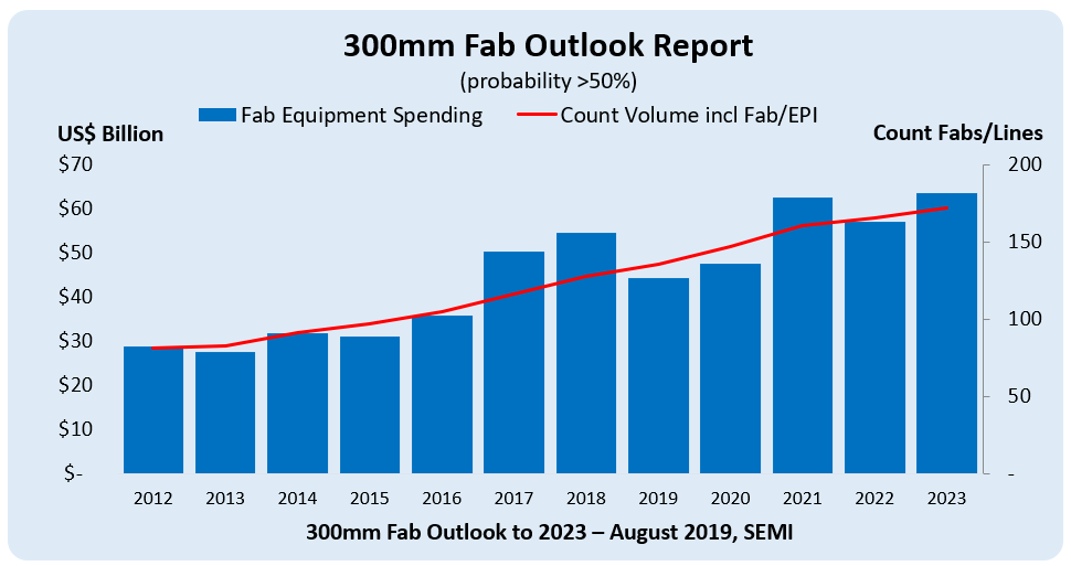
MILPITAS, Calif. — September 3, 2019 — 300mm fab equipment spending will slowly recover in 2020 after the 2019 downturn and take off in 2021 to log a new record high topping US$60 billion, only to lag again in 2022 and rebound to an all-time peak in 2023, according to the SEMI Industry Research and Statistics group in its first edition of the 300mm Fab Outlook report.

semi-logo

Most of the surges in fab equipment investment over the five-year outlook will be driven by memory (primarily NAND), foundry/logic, and power. Korea will head the list of top-spending regions followed by Taiwan and China, though Europe/Mideast and Southeast Asia are also expected to show healthy increases between 2019 and 2023.

Offering projections through 2023, the 300mm Fab Outlook report details fab investments across construction and equipment, as well as fab capacities and technologies investment for DRAM, NAND, foundry, logic, and a host of other products manufactured on 300mm wafers.

Fab equipment spending and volume fabs/lines count 2012-2023 and high-probability fab projects

The number of semiconductor fabs/lines in operation is expected to jump more than 30 percent, from 136 in 2019 to 172 in 2023, and climb even higher, to nearly 200, when lower probability fabs/lines are included in the count.

The new SEMI 300mm Fab Outlook report shows facility details by quarter through 2023 and also includes projections for fab projects through 2030 with estimates of various probabilities. 

To learn more about the SEMI 300mm Fab Outlook report, click here.

About SEMI
SEMI® connects more than 2,100 member companies and 1.3 million professionals worldwide to advance the technology and business of electronics design and manufacturing. SEMI members are responsible for the innovations in materials, design, equipment, software, devices, and services that enable smarter, faster, more powerful, and more affordable electronic products. Electronic System Design Alliance (ESD Alliance), FlexTech, the Fab Owners Alliance (FOA) and the MEMS & Sensors Industry Group (MSIG) are SEMI Strategic Association Partners, defined communities within SEMI focused on specific technologies. Visit www.semi.org to learn more, contact one of our worldwide offices, and connect with SEMI on LinkedIn and Twitter.

Association Contact
Michael Hall/SEMI
Phone: 1.408.943.7988
Email: [email protected]


MILPITAS, Calif. — August 22, 2019 — North America-based manufacturers of semiconductor equipment posted $2.03 billion in billings worldwide in July 2019 (three-month average basis), according to the July Equipment Market Data Subscription (EMDS) Billings Report published today by SEMI . The billings figure is 0.4 percent higher than the final June 2019 level of $2.03 billion, and is 14.5 percent lower than the July 2018 billings level of $2.38 billion.

SEMI Logo

“Total billings of North American equipment manufacturers for July were slightly up over June billings,” said Ajit Manocha, president and CEO of SEMI. “Demand for semiconductor equipment this year is being driven by leading-edge logic and foundry, though memory segment growth is soft due to weak market sentiment.”

The SEMI Billings report uses three-month moving averages of worldwide billings for North American-based semiconductor equipment manufacturers. Billings figures are in millions of U.S. dollars.

February 2019

Billings
(3-mo. avg.)

Year-Over-Year
February 2019 $1,868.1 -22.7%
March 2019 $1,825.3 -24.9%
April 2019 $1,922.0 -28.5%
May 2019 $2,065.2 -23.6%
June 2019 (final) $2.026.1 -18.4%
July 2019 (prelim) $2,034.2 -14.5%

Source: SEMI ( www.semi.org ), August 2019

SEMI publishes a monthly North American Billings report and issues the Worldwide Semiconductor Equipment Market Statistics (WWSEMS) report in collaboration with the Semiconductor Equipment Association of Japan (SEAJ). The WWSEMS report currently reports billings by 24 equipment segments and by seven end market regions. SEMI also has a long history of tracking semiconductor industry fab investments in detail on a company-by-company and fab-by-fab basis in its World Fab Forecast and SEMI FabView databases . These powerful tools provide access to spending forecasts, capacity ramp, technology transitions, and other information for over 1,000 fabs worldwide. For an overview of available SEMI market data, please visit www.semi.org/en/MarketInfo .

The data contained in this release were compiled by David Powell, Inc., an independent financial services firm, without audit, from data submitted directly by the participants. SEMI and David Powell, Inc. assume no responsibility for the accuracy of the underlying data.

About SEMI

SEMI® connects more than 2,100 member companies and 1.3 million professionals worldwide to advance the technology and business of electronics design and manufacturing. SEMI members are responsible for the innovations in materials, design, equipment, software, devices, and services that enable smarter, faster, more powerful, and more affordable electronic products. Electronic System Design Alliance (ESD Alliance), FlexTech, the Fab Owners Alliance (FOA) and the MEMS & Sensors Industry Group (MSIG) are SEMI Strategic Association Partners, defined communities within SEMI focused on specific technologies. Visit www.semi.org to learn more, contact one of our worldwide offices, and connect with SEMI on LinkedIn and Twitter .


Association Contact

Michael Hall/SEMI
Phone: 1.408.943.7988
Email: [email protected]

Notes

Next SEMI Billings report is September 19, 2019 at 3:00pm Pacific

For information on SEAJ Book-to-Bill Report, visit www.seaj.or.jp

GRENOBLE, France – 19 August, 2019 – SEMI Europe today announced finalists for the Technology Showcase for MEMS & Sensors and the Technology Showcase for Imaging Sensors at SEMI MEMS & Imaging Sensors Summit, 25-27 September, 2019 in Grenoble, France. The finalists are innovators of leading-edge MEMS and imaging sensors for applications spanning wireless sensor nodes in harsh environments, secure-by-design Internet of Things (IoT) devices, non-invasive wrist-worn blood glucose monitors, and 3D eye tracking that more naturally captures user attention in consumer devices. Registration is open now.

Selected by a committee of industry experts, Technology Showcase finalists will demonstrate new enabling products and platforms that are advancing MEMS and imaging sensors in biomedical, IoT, transportation, vision systems, and other consumer and industrial markets as they compete for audience votes. The Technology Showcases will take place during concurrent sessions on 26 September. Winners will be announced that evening during the gala dinner.
MEMS & Sensors Technology Showcase Finalists

  • frec|n|sys SAS: Wireless SAW Sensors at 2.45 GHz Built on POI Wafers — frec|n|sys’ Piezoelectric-on-insulator (POI) wafers represent a breakthrough for the development of modern surface acoustic wave (SAW) devices in wireless sensor applications, supporting sensor operation in difficult conditions such as closed metallic areas or for long-distance interrogation. Presented by Sylvain Ballandras, CEO, frec|n|sys SAS.


frec|n|sys SAS Logo
  • Marvin Test Solutions: Metal Oxide (MOX) Gas Sensor Testing — A precision test solution that accommodates very large site counts (512 devices) and matches the throughput of high-performance semiconductor test systems but at a lower cost. Presented by Victor Fernandes, European sales manager, Marvin Test Solutions.


Marvin Test Solutions Logo
  • Okmetic Oy: Industrial Patterning Platform for Value-added Si Substrate Manufacturing — The Okmetic platform advances the reliability, quality and performance of silicon-based devices. The platform is designed for MEMS, sensor and photonics applications requiring buried cavities, poly-Si filled through-silicon via (TSV) connections, or patterned multi-layer SOI design. Presented by Päivi Sievilä, customer support engineer, Okmetic Oy.


Okmetic Logo
  • Sensry GmbH: Building the IoT System of the Future with Sensry — Sensry’s individual sensor node features a new secure-by-design chip with flexible, customizable hardware configurations in a system in package (SiP). The sensor node is scalable to support the billions of IoT devices expected over the coming decades. Presented by Konrad Herre, CEO, Sensry GmbH.


Sensry Logo


  • Siconnex customized solutions GmbH: Fab Cost Saving Programs with BATCHSPRAY® Technology — Siconnex offers a wide spectrum of wet process solutions for etching, stripping and cleaning applications to help device makers reduce fab costs. Siconnex’s SicOzone™ technology helps reduce chemicals use, minimize chemical waste, enhance product quality,  improve user safety and reduce cleanroom space requirements. Presented by Fabio Wörndl, global director of sales and marketing.


Siconnex Logo

 Imaging and Sensors Technology Showcase Finalists

  • Alertgy: Impedance/Dielectric Spectrum Imaging System for Non-Invasive Continuous Glucose Monitor (NICGM) for Diabetics — Combines proprietary dielectric materials and signal processing/extraction to detect unique chemical signatures related to blood glucose levels – all in a tiny non-invasive platform suitable for integration in smart watches and other wrist-worn wearables. Presented by Marc Rippen, founder and president, Alertgy.


Alertgy Logo
  • Eyeware: 3D Eye Tracking Software for Depth-Sensing Cameras — Leverages off-the-shelf depth-sensing cameras to enable 3D eye-tracking in consumer devices, computers and cars without requiring users to wear glasses. The cameras instantly and naturally track user attention and intent. Presented by Bastjan Prenaj, co-founder and growth, Eyeware.


Eyeware Logo
  • Insightness AG: 7.2µm Pixel Event-Based Vision Sensor with Frame Readout — A stacked event-based image sensor that compresses visual information in smart pixels to enable vision sensors with low power consumption, fast response and high dynamic range. Providing 1024x768 resolution in an optical format of just 1 to 1.7 inches, the Insightness sensors support integration into compact camera modules. Presented by Raphael Berner, head of chip design, Insightness AG.


Insightness Logo

The MEMS & Imaging Sensors Summit returns to the WTC in Grenoble, France.
Stay in touch on Twitter @SEMIEurope: #SensorsSummit #MEMS #Imaging #IoT #AI #SEMIEurope
Premier Sponsors

For more information including the full event agenda, please visit the SEMI MEMS & Imaging Sensors Summit website.

About SEMI
SEMI® connects more than 2,100 member companies and 1.3 million professionals worldwide to advance the technology and business of electronics design and manufacturing. SEMI members are responsible for the innovations in materials, design, equipment, software, devices, and services that enable smarter, faster, more powerful, and more affordable electronic products. Electronic System Design Alliance (ESD Alliance), FlexTech, the Fab Owners Alliance (FOA) and the MEMS & Sensors Industry Group (MSIG) are SEMI Strategic Association Partners, defined communities within SEMI focused on specific technologies. Visit www.semi.org to learn more, contact one of our worldwide offices, and connect with SEMI on LinkedIn and Twitter.


Press Contact
Serena Brischetto/SEMI Europe
Email: [email protected]


In the long unfolding arc of technology innovation, artificial intelligence (AI) looms immense. In its quest to mimic human behavior, the technology touches energy, agriculture, manufacturing, logistics, healthcare, construction, transportation and nearly every other imaginable industry – a defining role that promises to fast track the fourth Industrial Revolution. And if the industry oracles have it right, AI growth will be nothing shy of explosive.“The gains these days are not incremental,” said Ajit Manocha, SEMI president and CEO, said to a gathering in July of the Chinese American Semiconductor Professional Association (CASPA) for its Summer Symposium at SEMI’s headquarters in Milpitas. “They are hockey stick – exponential – with AI semiconductors growing in market size from $4 billion this year to $70 billion in 2025.”Manocha left little doubt that AI is remaking the semiconductor industry and, in the process, the world at large. Internet of Things (IoT) and 4G/5G, both key AI enablers, will account for more than 75 percent of device connections by 2025.“Today, 30 billion devices worldwide are connected,” Manocha said, citing an Applied Materials prediction that the number of connected devices globally will grow to between 500 billion and 1 trillion by 2030. Those devices will generate stunning amounts of data collected, interpreted and used to reason, solve problems, learn and plan, leading to the holy grail of autonomous machine behavior.To process this colossal amount of data central to the promise of AI, the industry must break through the limits of a key technology: memory. Memory a Critical AI BottleneckThe challenge for memory starts with performance. Historically, every decade gains in compute performance have outpaced improvements in memory speed by 100 times, and over the past 20 years that gap has grown, said Steven Woo, a fellow and distinguished inventor at Rambus, presenting at the symposium. The upshot is that memory has bottlenecked compute and, in turn, AI performance. The industry has responded with new ways to implement memory systems on AI chips. Each is suited to unique performance requirements and, of course, comes with trade-offs. Among the frontrunners: On-chip memory delivers the highest bandwidth and power efficiency but is limited in capacity. HBM (High Bandwidth Memory) offers both very high memory bandwidth and density. GDDR balances trade-offs among bandwidth, power efficiency, cost and reliability. Since 2012, AI training capability has grown 300,000 times, besting Moore’s law by 25,000 times in doubling every 3.5 months, a blistering pace compared to the 18-month doubling cycle of Moore’s law, Woo said. The staggering improvements have been driven by parallel computing capacity and new application-specific silicon like Google’s Tensor Processing Unit (TPU).These specialized silicon architectures and parallel engines are key to sustaining future gains in compute performance and combatting the slowing of Moore’s Law and the end of power scaling, Woo said. By rethinking the way processors are architected for certain markets, chipmakers can develop dedicated hardware capable of operating with 100 to 1,000 times greater energy efficiency than general purpose processors to overcome another big limiter to scaling compute performance – power.For its part, the memory industry can improve performance by signaling at higher data rates and using stacked architectures like HBM for greater power efficiency and performance, and by bringing compute closer to the data.Memory scaling for AIA key challenge is scaling memory for AI. Demand for better voice, gesture and facial recognition experiences and more immersive virtual reality and augmented reality interactions is tremendous, said Bill En, senior director at AMD, speaking at the symposium. These capabilities require more processing power across both high-performance computing (HPC) for big data analytics and machine learning as it relies on AI and machine intelligence to generate meaningful insights. Emerging machine learning applications include classification and security, medicine, advanced driver assistance, human-aided design, real-time analytics and industrial automation. And with 75 billion IoT-connected devices – all generating data – expected by 2025, there will be no shortage of data to analyze, En said. The wings alone of a new Airbus A380-1000 feature some 10,000 sensors.Mountains of this data are stored in massive data centers on magnetic hard drives, then transferred to DRAM before moving to SRAM within the CPU for the handoff to the compute hardware for analysis.With data growing at an exponential clip, the question is how to make sure all other memory systems can handle the flood of data. AMD’s answer is a chiplet architecture featuring eight smaller chips around the edge that drive the compute and a large chip in the center that doubles the IO interface and memory capability to in turn double chip bandwidth.AMD has also moved from a legacy GDDR5 memory chip configuration to HBM to bring memory bandwidth closer to the GPU for more efficient processing of AI applications. The HBM provides much higher bandwidth while reducing power consumption. Compared to DRAM, AMD’s HBM delivers a much faster data rate and far greater memory density, En said.Over the next decade, look for more performance improvements from multi-chip architectures, innovations in memory technology and integration, aggressive 3D stacking and streamlined system-level interconnects, he said. The industry will also continue to drive performance gains in devices, compute density and power through technology scaling.Michael Hall is a global marketing communications manager at SEMI.
Read More

SEMI Technology Think Tank Summit and Electro-Innovation Forum debut. Top research institute experts and tech leaders to help lay foundation for future of innovation and microelectronics.

TAIPEI, Taiwan ─ August 13, 2019 ─ Spanning the entire semiconductor and microelectronics supply chain – from design through systems – SEMICON Taiwan 2019 will gather the world’s top technologists, visionaries and innovators for insights into the latest trends and opportunities across smart vertical markets including manufacturing, automotive, healthcare and data. September 18-20 at Nangang Exhibition Center, Hall I, in Taipei, SEMICON Taiwan 2019 will mark the debut of the SEMI Electro-innovation Forum and Technology Think Tank Summit. Registration for SEMICON Taiwan is open.

  •  
    SEMICON Taiwan Logo
    Electro-innovation Forum – Experts from five of the world’s top research institutes and R&D centers will examine innovation drivers and trends and prospects for the microelectronics industry. Participants will include imec, CEA-Leti, Fraunhofer, the National Research Foundation (NRF), the Industrial Technology Research Institute (ITRI) and TSMC.
  •  Technology Think Tank Summit – Co-organized with the Ministry of Economic Affairs (MOEA), the summit will feature industry leaders in SiP, IC design, memory, wafer fabrication, packaging and testing exploring the future of the industry. Participants include CEOs from Quanta Computer, Hon Hai Technology Group, TSMC, ASE, Etron Technology, Powerchip Semiconductor and Macronix International.

International Forums for Insights on Industry Trends

The two events are among 21 international forums on industry trends and the latest technologies at SEMICON Taiwan 2019 featuring renowned speakers from diverse disciplines. Themed Leading the SMART Future, SEMICON Taiwan will spotlight Artificial intelligence (AI), Internet of Things (IoT), 5G, machine learning, quantum computing and other cutting-edge technologies that are transforming the microelectronics industry and giving rise to a growing universe of smart applications. AI alone spans energy, agriculture, manufacturing, logistics, healthcare, construction, transportation and nearly every other industry – a defining role that promises to fast track the fourth Industrial Revolution.

The following SEMICON Taiwan forums, summits and pavilions will offer the latest industry perspectives on key vertical markets and the talent vital to industry growth.

  •  Smart Transportation Forum – Covers issues including 5G and AI for Future Mobility, Mapping for Autonomous Driving, and Next-Generation Communications in the Self-Driving Era
  •  Smart Data Global Summit – Latest electronics system design technologies
  •  Smart MedTech Forum – Explores the future of smart medical technology and business opportunities
  •  Smart Manufacturing Show – Showcases complete smart manufacturing solutions for a wide range of high-technology industries such as semiconductor, touch panel, flat-panel display and PCB
  •  Smart Workforce Pavilion – Semiconductor industry insights, lectures, career coaching and job matching

One of the world’s largest and most influential high-technology events, SEMICON Taiwan will feature:

  •  21 theme areas and national pavilions
  •  More than 200 speakers across 21 international forums
  •  700 exhibitors from around the world
  •  More than 2,200 booths

SEMICON Taiwan 2019 showcases the full suite of SEMI offerings spanning the full electronics supply chain to support industry growth including:

  •  Vertical Application Platforms: Smart Manufacturing, Smart Transportation, Smart Medical, Smart Data and IoT
  •  Workforce Development, Industry Standards, Think Tanks and Thought Leadership Platforms
  •  Strategic Association Partners such as R&D and innovation leaders imec, CEA-Leti and Fraunhofer as well as MEMS & Sensors Industry Group and Electronic System Design Alliance

Record-Setting Attendance

SEMICON Taiwan is expected to draw an event record 50,000 visitors as Taiwan remains atop the world in semiconductor equipment spending at US$11.4 billion and a 21.1 percent CAGR on the strength of the region’s advanced manufacturing capabilities. A global hub of wafer production and IC packaging, Taiwan claims the top spot in semiconductor equipment spending for the ninth consecutive year.

With the semiconductor industry working to extend silicon scaling beyond Moore’s Law, SEMICON Taiwan will also gather industry experts to explore heterogeneous integration opportunities and challenges across three events:

For more information, please visit the SEMICON Taiwan 2019 website or follow us on Facebook.

About SEMI

SEMI® connects more than 2,100 member companies and 1.3 million professionals worldwide to advance the technology and business of electronics design and manufacturing. SEMI members are responsible for the innovations in materials, design, equipment, software, devices, and services that enable smarter, faster, more powerful, and more affordable electronic products. Electronic System Design Alliance (ESD Alliance), FlexTech, the Fab Owners Alliance (FOA) and the MEMS & Sensors Industry Group (MSIG) are SEMI Strategic Association Partners, defined communities within SEMI focused on specific technologies. Visit www.semi.org to learn more, contact one of our worldwide offices, and connect with SEMI on LinkedIn and Twitter.

Association Contacts

Emmy Yi
E-mail:
[email protected]
Tel: +886.3.560.1777 ext.205

Eileen Lin
E-mail:
[email protected]
Tel: +886.3.560.1777 ext. 288


Like all other SEMICON expositions, SEMICON West last month gathered thousands of people to make business connections and learn about the industry and its opportunities. But the events are also great venues for SEMI’s Global Industry Advocacy team to meet with industry leaders from around the world as well as regional SEMI presidents to discuss policy issues we face in each region and best practices for how to address them. The time was also ripe for us to meet with various advisory groups and advocacy committees to examine current issues.Top on our list at SEMICON West was a discussion with SEMI’s International Board of Directors about the then newly announced actions by Japan’s Ministry of Economy, Trade and Industry (METI) to tighten export controls in trade with Korea. SEMI depends heavily on and is grateful for insights from its International Board, Board of Industry Leaders and various Regional Advisory Boards. They are crucial to our ability to develop and execute industry advocacy strategies that take into account regional idiosyncrasies, geopolitical sensitivities and global supply chain complexities. SEMI is unique in its ability to bring a global perspective to engaging governments around the world in real time. In the case of the trade dispute between Japan and South Korea, we engaged SEMI members in Japan and Korea as we developed our strategy.On the SEMI America’s front, the North American Advisory Board and its Public Policy Committee met at SEMICON West for a spirited discussion on how to best manage our lobbying activities and how regional and U.S. companies should be involved. The committee’s perspectives and guidance will be invaluable as we chart a path forward in these challenging times in global trade.Our Global Industry Advocacy team also continues to build out SEMI Works, SEMI’s comprehensive initiative to develop a talent pipeline and overcome the industry’s longstanding shortage of skilled workers. SEMI Works focuses on stimulating greater interest in STEM careers, aligning STEM course curriculum and industry needs, and connecting students with relevant courses and careers. We are in the process of launching three regional pilot programs that will enable us to develop the SEMI Works business model that we’ll use to scale the program and ensure the initiative is robust and sustainable. At SEMICON West the Global Advocacy team convened regional stakeholders involved in these pilots to share information on opportunities and challenges and to discuss various implementation strategies.At SEMICON West we also facilitated meetings with U.S. government representatives aimed at improving cybersecurity in manufacturing and developing a commercial security model that will strengthen security throughout the supply chain in areas vital to industry growth such as traceability.After nearly 50 years, SEMI still excels in enabling the industry collaborations key to growth and innovation. Collaboration is also a driving force within SEMI Global Industry Advocacy as we continue to work with SEMI members, our various boards and governments around the world to advance the interests of the semiconductor industry.Mike Russo is vice president of Global Industry Advocacy at SEMI.
Read More
The U.S. on September 1 will levy a 10 percent tariff on $300 billion (List 4) worth of Chinese goods that until now were exempt from duties, President Trump said today. The trade action makes good on the U.S. president’s commitment to impose the new round tariffs in response to China’s failure to deliver on promises to buy more U.S. farm goods and to stop the flow of the painkiller fentanyl into the U.S. The 25 percent tariffs already in effect on $250 billion in goods will remain in place.The new list includes items used in the electronics industry but also encompasses retail products spanning the U.S. economy including clothing, toys and cell phones, exacting a more direct hit to U.S. consumers. A meeting between China and U.S. trade officials in Shanghai this week apparently did little to ease trade tensions. Both sides plan to meet again in September, though expectations for meaningful progress toward resolving their trade differences then are low.The U.S. believes China backtracked from commitments to changing its practices related to forced technology transfer and intellectual property theft. China denies making the pledges and insists on the removal of all tariffs as part of a settlement.The U.S. actions risk backlash from China including non-tariff barriers to trade such as licensing delays, more stringent business-related inspections, and an accelerated rollout of its unreliable entities list, China’s response to the U.S. decision to blacklist telecommunications giant Huawei. The list includes foreign companies, other organizations and individuals that China sees as national security threats or risks to China’s economy.SEMI will continue to urge both nations to reach an agreement consistent with its 10 Principles for the Global Semiconductor Supply Chain in Modern Trade Agreements. The principles encourage free and fair trade, open markets, and respect of IP among all players in the global electronics manufacturing supply chain.SEMI member companies impacted by the new U.S. tariffs or facing any new non-tariff barriers in China should contact Jay Chittooran, public policy manager in SEMI’s Global Advocacy Office, at [email protected] Russo is vice president of Global Industry Advocacy at SEMI.
Read More
On July 1st, Japan’s Ministry of Economy, Trade and Industry (METI) announced updated licensing policies and procedures on the export and transfer of controlled items and their relevant technologies to the Republic of Korea (ROK). METI’s stated purpose for the actions were “in order to ensure appropriate implementation of export control.”In particular, METI will tighten controls on certain items and their relevant technologies as follows: Remove the ROK from its “white list” of trusted partners, limiting the ROK’s preferential treatment for exports Mandate individual licenses for exports of certain chemicals including fluorinated polyimide, photoresist, and hydrogen fluoride – all used in semiconductor and electronics manufacturing – and technology transferred with exports of manufacturing equipment to the ROK. Bulk licenses for the chemicals will no longer be available. METI has indicated that its actions were not intended as punitive, but rather as necessary to ensure proper management of the export control system and the effective tracking of chemicals, materials and technologies that could be used to develop weapons of mass destruction (WMDs). Nevertheless, the trade actions are cause for concern as they could have a negative impact on our members operating in Korea and Japan and the global supply chain in general.After the METI announcement, SEMI immediately consulted its International Board of Directors and assembled a global advocacy response team comprised of SEMI member companies and SEMI regional presidents in both Japan and Korea to assess risks to SEMI members operating in both regions and to the industry’s global supply chain. Additionally, SEMI conveyed its concerns to Japan and ROK trade officials, stressing that the semiconductor industry will bear the brunt of the new measures if the trade dispute escalates.SEMI president and CEO Ajit Manocha said: “We informed both governments of potential impacts of an escalation to SEMI members, their economies and the global supply chain and are encouraging them to resolve their differences. SEMI’s focus is to ensure the global microelectronics supply chain remains strong and intact.”SEMI member companies have stated that METI and the Japan government have provided assurances that trade with the ROK will not be encumbered and that semiconductor companies will see minimal impact regarding export license approvals. To this end, SEMI will continue to engage our members in Korea and Japan, monitor the dispute as it continues to unfold, and facilitate regular meetings between industry and the involved governments to ensure that industry impacts are identified and risks are mitigated. In the event the dispute escalates, SEMI is prepared to take action in accordance with its Global Trade Principles.SEMI released its Global Trade Principles last year to provide guidance to governments around the world in developing policies that benefit both regional economies and the industry. These trade principles are based on SEMI’s four trade pillars of free and fair trade, open markets, supply chain growth, and respect for IP and national security.Member companies negatively impacted by any changes in Japan’s regulatory policies or with any questions should contact their regional SEMI office or Jay Chittooran, Public Policy Manager, SEMI Global Advocacy, at [email protected] Russo is Vice President of Global Industry Advocacy at SEMI.
Read More

MILPITAS, Calif. — July 25, 2019 — North America-based manufacturers of semiconductor equipment posted $2.01 billion in billings worldwide in June 2019 (three-month average basis), according to the June Equipment Market Data Subscription (EMDS) Billings Report published today by SEMI. The billings figure is 2.5 percent lower than the final May 2019 level of $2.07 billion, and is 19 percent lower than the June 2018 billings level of $2.48 billion.

semi-logo

“June billings of North American equipment manufacturers fell nearly three percent when compared to the prior month,” said Ajit Manocha, president and CEO of SEMI. “While billings weakened for the most recent month, total global billings of suppliers based in North America for the most recent quarter are stronger than their first-quarter 2019 billings.”

The SEMI Billings report uses three-month moving averages of worldwide billings for North American-based semiconductor equipment manufacturers. Billings figures are in millions of U.S. dollars.


Billings
(3-mo. avg.)

Year-Over-Year

January 2019

$1,896.3

-20.0%

February 2019

$1,868.1

-22.7%

March 2019

$1,825.3

-24.9%

April 2019

$1,922.0

-28.5%

May 2019 (final)

$2,065.2

-23.6%

June 2019 (prelim)

$2,012.7

-19.0%


SEMI publishes a monthly North American Billings report and issues the Worldwide Semiconductor Equipment Market Statistics (WWSEMS) report in collaboration with the Semiconductor Equipment Association of Japan (SEAJ). The WWSEMS report currently reports billings by 24 equipment segments and by seven end market regions. SEMI also has a long history of tracking semiconductor industry fab investments in detail on a company-by-company and fab-by-fab basis in its World Fab Forecast and SEMI FabView databases. These powerful tools provide access to spending forecasts, capacity ramp, technology transitions, and other information for over 1,000 fabs worldwide. For an overview of available SEMI market data, please visit www.semi.org/en/MarketInfo.

The data contained in this release were compiled by David Powell, Inc., an independent financial services firm, without audit, from data submitted directly by the participants. SEMI and David Powell, Inc. assume no responsibility for the accuracy of the underlying data.

About SEMI

SEMI® connects more than 2,100 member companies and 1.3 million professionals worldwide to advance the technology and business of electronics design and manufacturing. SEMI members are responsible for the innovations in materials, design, equipment, software, devices, and services that enable smarter, faster, more powerful, and more affordable electronic products. Electronic System Design Alliance (ESD Alliance), FlexTech, the Fab Owners Alliance (FOA) and the MEMS & Sensors Industry Group (MSIG) are SEMI Strategic Association Partners, defined communities within SEMI focused on specific technologies. Visit www.semi.org to learn more, contact one of our worldwide offices, and connect with SEMI on LinkedIn and Twitter.

Association Contact

Michael Hall/SEMI
Phone: 1.408.943.7988
Email: [email protected]

Notes Next SEMI Billings report is August 22, 2019 at 3:00pm Pacific For information on SEAJ Book-to-Bill Report, visit www.seaj.or.jp

Milpitas, Calif. — July 29, 2019 — With advanced materials now a critical enabler of semiconductor growth applications, the stage is set for Strategic Materials Conference (SMC 2019), the premier event offering the latest market insights into drivers of advanced materials in the microelectronics supply chain. September 23-25, 2019, in San Jose, Calif., SMC will highlight opportunities and demand for key enabling materials in every segment of the electronics supply chain. SMC 2019 registration is open.

SMC North America Logo

Themed Year of Transition, Material Opportunities and Challenges, SMC gathers top executives from every segment of semiconductor manufacturing to provide the latest developments in areas of advanced materials including:

  • Economic and Market Trends
  • Silicon and Alternative Substrates
  • More than Moore
  • Emerging Materials and Applications
  • Automotive IC Drives Material Growth
  • Fabs of the Future

SMC 2019 Keynotes

Dragos Maciuca Photo
Dragos Maciuca, PhD, Executive Technical Director, Palo Alto Research and Innovation Center
Ford Logo
Carlos H. Diaz, PhD, Senior Director, Corporate Research
TSMC Logo
Bertrand Loy Photo
Bertrand Loy, President and CEO
Entegris Logo

Industry leaders presenting at SMC 2019 also include:

  • Applied Materials
  • Advanced Semiconductor Engineering (ASE)
  • DuPont
  • GLOBALFOUNDRIES
  • IBM Research
  • IMEC
  • Intel Corporation
  • Micron Technology
  • ON Semiconductor
  • PowerAmerica
  • Siltronic Corporation
  • Wolfspeed, A Cree Company 

Part of the SEMI Technology Leadership Series of the Americas, this year’s event, at the Double Tree by Hilton, also features exclusive business networking for exploring collaboration opportunities in the extended electronics ecosystem and the pre-conference welcome reception, Monday, September 23, 5:30pm - 7:00pm. More event information is available at SMC 2019.


About SEMI
SEMI® connects more than 2,100 member companies and 1.3 million professionals worldwide to advance the technology and business of electronics design and manufacturing. SEMI members are responsible for the innovations in materials, design, equipment, software, devices, and services that enable smarter, faster, more powerful, and more affordable electronic products. Electronic System Design Alliance (ESD Alliance), FlexTech, the Fab Owners Alliance (FOA) and the MEMS & Sensors Industry Group (MSIG) are SEMI Strategic Association Partners, defined communities within SEMI focused on specific technologies. Visit www.semi.org to learn more, contact one of our worldwide offices, and connect with SEMI on LinkedIn and Twitter.

Association Contact

Michael Hall/SEMI
Phone: 1.408.943.7988
Email: [email protected]

Scott Stevens, Cardinal Communications for SEMI Americas
Phone: 1.512.288.4050
Email: [email protected]