





MILPITAS, Calif. — December 3, 2019 — Worldwide semiconductor equipment manufacturers posted third-quarter 2019 billings of US$14.9 billion, a quarter-over-quarter increase of 12 percent but down 6 percent from the third quarter of 2018, SEMI, the global industry association representing the electronics manufacturing and design supply chain, reported today.

The data are gathered jointly with the Semiconductor Equipment Association of Japan (SEAJ) from more than 80 global equipment companies that provide data on a monthly basis.
The quarterly billings data by region in billions of U.S. dollars, and quarter-over-quarter and year-over-year growth rates by region, are as follows:
|
|
3Q2019 |
2Q2019 |
3Q2018 |
3Q19/2Q19 |
3Q19/3Q18 |
|
Taiwan |
3.90 |
3.21 |
2.90 |
21% |
34% |
|
China |
3.44 |
3.36 |
3.98 |
2% |
-14% |
|
North America |
2.49 |
1.70 |
1.27 |
47% |
96% |
|
Korea |
2.20 |
2.58 |
3.45 |
-15% |
-36% |
|
Japan |
1.67 |
1.38 |
2.41 |
21% |
-30% |
|
Rest of World |
0.76 |
0.51 |
0.98 |
48% |
-23% |
|
Europe |
0.39 |
0.57 |
0.85 |
-31% |
-54% |
|
Total |
14.86 |
13.31 |
15.84 |
12% |
-6% |
Source: SEMI (www.semi.org) and SEAJ, December 2019
The Equipment Market Data Subscription (EMDS) from SEMI provides comprehensive market data for the global semiconductor equipment market. A subscription includes three reports:
- Monthly SEMI Billings Report, a perspective of trends in the equipment market
- Monthly Worldwide Semiconductor Equipment Market Statistics (WWSEMS), a detailed report of semiconductor equipment billings for seven regions and 24 market segments
- SEMI Total OEM Semiconductor Equipment Forecast, an outlook for the semiconductor equipment market
For more information or to subscribe, please contact SEMI customer service at 1.877.746.7788 (toll free in the U.S.) or 1.408.943.6901 (International Callers). More information is also available online.
About SEMI
SEMI® connects more than 2,100 member companies and 1.3 million professionals worldwide to advance the technology and business of electronics design and manufacturing. SEMI members are responsible for the innovations in materials, design, equipment, software, devices, and services that enable smarter, faster, more powerful, and more affordable electronic products. Electronic System Design Alliance (ESD Alliance), FlexTech, the Fab Owners Alliance (FOA) and the MEMS & Sensors Industry Group (MSIG) are SEMI Strategic Association Partners, defined communities within SEMI focused on specific technologies. Visit www.semi.org to learn more, contact one of our worldwide offices, and connect with SEMI on LinkedIn and Twitter.
Association Contact
Michael Hall/SEMI
Phone: 1.408.943.7988
Email: [email protected]
MILPITAS, CA — December 2, 2019 — SEMI today announced that Mitsunobu (Nobu) Koshiba of JSR Corporation has won the SEMI Sales and Marketing Excellence Award, inspired by Bob Graham, for 2019. The 22nd recipient of the award, Koshiba will be honored for his role in developing and bringing to market multiple photoresist generations that have been critical to the semiconductor industry. He will be recognized during ceremonies at SEMICON Japan 2019, December 11-13, at Tokyo Big Sight in Tokyo.
Photoresist innovations have enabled the continued scaling of semiconductor dimensions and power profiles. Koshiba’s focus on 193nm dry, 193nm immersion and extreme ultraviolet lithography (EUV) resists – all vitally important to JSR Corporation customers – accelerated their development. He served as a key bridge between JSR Corporation’s research and development initiatives and its customers in aligning the company with their needs. Koshiba also led the important pivot from 157nm to 193nm immersion.
“SEMI is proud and grateful to count Mitsunobu Koshiba among our most inspirational and progressive industry leaders,” said Ajit Manocha, president and CEO of SEMI. “His vision, resolve and innovative spirit have been instrumental in advancing our industry. Today, SEMI and its membership honor Koshiba-san for his major contributions to semiconductor manufacturing."
The SEMI Sales and Marketing Excellence Award was inspired by the late Bob Graham, the distinguished semiconductor industry leader, who was a member of the founding team of Intel. Graham also helped establish industry-leading companies such as Applied Materials and Novellus Systems. The award was established to honor individuals for the creation and/or implementation of marketing programs that enhance customer satisfaction and further the growth of the semiconductor equipment and materials industry.
Eligible candidates are nominated by their industry peers and selected after due diligence by the SEMI Sales and Marketing Excellence Award Committee. Previous recipients of this award include: Luc Van den hove (2018), Toshio Maruyama (2017), Jim Bowen (2016), Terry (Tetsuro) Higashi (2015), Winfried Kaiser (2014), Joung Cho (JC) Kim (2013), G. Dan Hutcheson (2012), Franz Janker (2011), Martin van den Brink (2010), Peter Hanley (2009), Richard Hong (2008), Richard E. Dyck (2007), Aubrey (Bill) C. Tobey (2006), Archie Hwang (2005), Edward Braun (2004), Shigeru (Steve) Nakayama (2003), Jerry Hutcheson and Ed Segal (2002), Jim Healy and Barry Rapozo (2001), and Art Zafiropoulo (2000).
About SEMI
SEMI® connects more than 2,100 member companies and 1.3 million professionals worldwide to advance the technology and business of electronics design and manufacturing. SEMI members are responsible for the innovations in materials, design, equipment, software, devices, and services that enable smarter, faster, more powerful, and more affordable electronic products. Electronic System Design Alliance (ESD Alliance), FlexTech, the Fab Owners Alliance (FOA) and the MEMS & Sensors Industry Group (MSIG) are SEMI Strategic Association Partners, defined communities within SEMI focused on specific technologies. Visit www.semi.org to learn more, contact one of our worldwide offices, and connect with SEMI on LinkedIn and Twitter.
Association Contact
Michael Hall/SEMI
Phone: 1.408.943.7988
Email:[email protected]
ISS 2020 kicks off SEMI’s 50th anniversary year with insights into business, economic and technology trends
MILPITAS, Calif. – November 25, 2019 – SEMI announced today that Industry Strategy Symposium (ISS) 2020 will take place January 12-15 at the Ritz-Carlton in Half Moon Bay, Calif. with the theme Data Driven Innovation and Growth. ISS is the year’s first executive check-in, offering perspectives from leading analysts, researchers, economists, and technologists on forces impacting the semiconductor industry. The annual symposium provides insights into growth opportunities and industry intelligence to help inform company business plans and forecasts based on current market conditions. Registration is now open.

The proliferation of smart connected devices continues as vast amounts of data is generated by the explosion of electronic devices, driving significant growth across all semiconductor segments. This hyper-connectivity is being fueled by innovations in Internet of Things (IoT), artificial intelligence (AI), 5G, machine learning and other advanced technologies. Connecting and collaborating across the expanding technology ecosystem has never been more important as the world turns to innovation to tackle some of its most pressing challenges.
“Top visionaries and other thought leaders will gather at ISS to deliver insights into the latest electronics industry developments and trends that will shape business planning for 2020,” said David Anderson, president of SEMI Americas and host of ISS. “Among the most popular of SEMI’s conferences for the C-suite, ISS gives senior executives from across the industry an intimate, first-hand look at what to expect in the year ahead.”
ISS 2020 is the first of eight conferences comprising SEMI’s second annual Technology Leadership Series of the Americas. Aligned from coast to coast throughout 2020, the series is designed to foster critical discussions on the short- and long-term challenges and opportunities in the $2 trillion global electronics industry.
ISS 2020 highlights include:
Keynotes
- Richard Gottscho, Executive Vice President and corporate Chief Technology Officer at Lam Research
- Simon Segars, Chief Executive Officer at Arm
Economic trends and market forces shaping the electronics industry
- Executives and economists from AlphaOne Capital, Bain & Company, Gartner, IHS Markit, Jefferies and VLSI Research
Insights into market and application drivers
- Top executives from Avrio Institute, Cabot, Entegris, Ericsson, Ford Motor Company, Google, International Business Strategies (IBS), Intuitive Surgical, Jiangsu Changjiang Electronics Technology, Lyft, Oxford Performance Materials, Qualcomm and Robert Bosch
SEMI Golden Anniversary
The year 2020 marks SEMI’s golden anniversary. For half a century, SEMI has brought the industry together to connect, collaborate and innovate, helping to transform the world with technologies that have profoundly enhanced many aspects of human lives. The golden anniversary celebration will honor legends of the past 50 years and innovators who will lead the electronics design and manufacturing industry into the next 50. The event will be held during SEMICON West 2020 at the Moscone Center in San Francisco, July 20-23.
About SEMI
SEMI® connects more than 2,100 member companies and 1.3 million professionals worldwide to advance the technology and business of electronics manufacturing. SEMI members are responsible for the innovations in materials, design, equipment, software, devices, and services that enable smarter, faster, more powerful, and more affordable electronic products. Electronic System Design Alliance (ESD Alliance), FlexTech, the Fab Owners Alliance (FOA) and the MEMS & Sensors Industry Group (MSIG) are SEMI Strategic Association Partners, defined communities within SEMI focused on specific technologies. Since 1970, SEMI has built connections that have helped its members prosper, create new markets, and address common industry challenges together. SEMI maintains offices in Bangalore, Berlin, Brussels, Grenoble, Hsinchu, Seoul, Shanghai, Silicon Valley (Milpitas, Calif.), Singapore, Tokyo, and Washington, D.C. For more information, visit www.semi.org and follow SEMI on LinkedIn and Twitter.
Association Contacts
Michael Hall/SEMI
Phone: 1.408.943.7988
Email: [email protected]
Scott Stevens, for SEMI Americas
Phone: 1.512.288.4050
Email: [email protected]
TOKYO – November 26, 2019 – Smart mobility, smart manufacturing and business continuity planning (BCP) will come into sharp focus at SEMICON Japan 2019 as players from across the electronics supply chain gather December 11-13 at Tokyo Big Sight for the latest technology developments and innovations fueling a smarter world. Registration for SEMICON Japan 2019 is open.

SMART Transportation
Automobiles are growing in technical sophistication thanks to increasing silicon content, adding connected navigation systems, Lidar, and other connected-car features including internet radio, mobile search and cloud-based content. According to IHS Markit, microcomponent ICs will grow the fastest over the coming years among all semiconductor device categories, driven by automated driving and the rising number of sensors.
In the SEMICON Japan 2019 SMART Applications Zone, the SMART Transportation Forum will highlight next-generation usage models such as Mobility-as-a-Service (MaaS), electrification and autonomous driving. Device manufacturers will showcase the latest research and development and software platforms, and market researchers will offer insights into automotive technology trends. The area will also feature an automobile equipped with autonomous driving software.
Key SMART Transportation exhibitors include TOYOTA, DENSO, ZUKEN, Tier IV, Renesas Electronics, LIVOX TECH, Deloitte Touche Tohmatsu and Solidray.
SMART Manufacturing
The SMART Applications Zone will also feature the SMART Manufacturing Forum, where Advanced Industrial Science and Technology (AIST) will demonstrate remote control of a Minimal Fab System, and Deloitte Touche Tohmatsu will take visitors on tour of a semiconductor manufacturing fab using augmented reality (AR) and virtual reality (VR).
Other key SMART Manufacturing exhibitors include SIEMENS, Sony Semiconductor Solutions, Chuo Denshi Kogyo (CDK) and United Semiconductor Japan (USJC).
Business Continuity Planning
Business Continuity Planning has seen strong demand as companies in the semiconductor manufacturing supply chain work to deepen their cooperation with each other to sustain operations in the event of natural disasters and other emergencies. SEMICON Japan 2019 will feature an exhibition and seminar highlighting the importance of BCP to the electronics supply chain. Visitors will learn about earthquake countermeasures by stepping into the Seismic Isolation Experience Car.
Exhibitors in the BCP area in West Hall 4 include THK, DISCO, HORIBA STEC and Murata Machinery.
Representatives from Sony Semiconductor Manufacturing, THK, DISCO and Team Engineering Consulting will share lessons learned from actual disasters and discuss the vital importance of daily preparation for disasters on December 12 in the Conference Tower, room 608.
For registration and other information, please visit the SEMICON Japan 2019 website.
About SEMI
SEMI® connects more than 2,100 member companies and 1.3 million professionals worldwide to advance the technology and business of electronics design and manufacturing. SEMI members are responsible for the innovations in materials, design, equipment, software, devices, and services that enable smarter, faster, more powerful, and more affordable electronic products. Electronic System Design Alliance (ESD Alliance), FlexTech, the Fab Owners Alliance (FOA) and the MEMS & Sensors Industry Group (MSIG) are SEMI Strategic Association Partners, defined communities within SEMI focused on specific technologies. Visit www.semi.org to learn more, contact one of our worldwide offices, and connect with SEMI on LinkedIn and Twitter.
Association Contact
Mayumi Amagai
Phone: 81-3-3222-5801
Email: [email protected]
MILPITAS, Calif. — November 19, 2019 — North America-based manufacturers of semiconductor equipment posted $2.11 billion in billings worldwide in October 2019 (three-month average basis), according to the October Equipment Market Data Subscription (EMDS) Billings Report published today by SEMI. The billings figure is 7.7 percent higher than the final September 2019 level of $1.96 billion, and is 3.9 percent higher than the October 2018 billings level of $2.03 billion.
“Monthly billings of North American equipment manufacturers registered their first year-over-year increase since October 2018 and are at their highest level since December of last year,” said Ajit Manocha, president and CEO of SEMI. “Equipment billings are accelerating on the strength of memory inventory drawdowns and foundry investments in leading-edge equipment.”
The SEMI Billings report uses three-month moving averages of worldwide billings for North American-based semiconductor equipment manufacturers. Billings figures are in millions of U.S. dollars.
|
|
Billings |
Year-Over-Year |
|
May 2019 |
$2,065.2 |
-23.6% |
|
June 2019 |
$2.026.1 |
-18.4% |
|
July 2019 |
$2,031.9 |
-14.6% |
|
August 2019 |
$2,001.8 |
-10.5% |
|
September 2019 (final) |
$1,959.1 |
-5.7% |
|
October 2019 (prelim) |
$2,109.1 |
3.9% |
Source: SEMI (www.semi.org), November 2019
SEMI publishes a monthly North American Billings report and issues the Worldwide Semiconductor Equipment Market Statistics (WWSEMS) report in collaboration with the Semiconductor Equipment Association of Japan (SEAJ). The WWSEMS report currently reports billings by 24 equipment segments and by seven end market regions. SEMI also has a long history of tracking semiconductor industry fab investments in detail on a company-by-company and fab-by-fab basis in its World Fab Forecast and SEMI FabView databases. These powerful tools provide access to spending forecasts, capacity ramp, technology transitions, and other information for over 1,000 fabs worldwide. For an overview of available SEMI market data, please visit www.semi.org/en/MarketInfo.
The data contained in this release were compiled by David Powell, Inc., an independent financial services firm, without audit, from data submitted directly by the participants. SEMI and David Powell, Inc. assume no responsibility for the accuracy of the underlying data.
About SEMI
SEMI® connects more than 2,100 member companies and 1.3 million professionals worldwide to advance the technology and business of electronics design and manufacturing. SEMI members are responsible for the innovations in materials, design, equipment, software, devices, and services that enable smarter, faster, more powerful, and more affordable electronic products. Electronic System Design Alliance (ESD Alliance), FlexTech, the Fab Owners Alliance (FOA) and the MEMS & Sensors Industry Group (MSIG) are SEMI Strategic Association Partners, defined communities within SEMI focused on specific technologies. Visit www.semi.org to learn more, contact one of our worldwide offices, and connect with SEMI on LinkedIn and Twitter.
Association Contact
Michael Hall/SEMI
Phone: 1.408.943.7988
Email: [email protected]
Notes
Next SEMI Billings report is December 19, 2019 at 3:00pm Pacific.
For information on SEAJ Book-to-Bill Report, visit www.seaj.or.jp
SEOUL, South Korea – November 19, 2019 – With Korea the world’s largest manufacturer of memory semiconductors and leading in 300mm fab construction in 2019, the region is paving the way to SEMICON Korea 2020 as more than 500 companies and 55,000 visitors are expected to gather February 5-7 at the COEX in Seoul for the latest microelectronics developments, innovations and trends powering the next wave of industry growth. Registration for SEMICON Korea, the premier event in Korea for electronics manufacturing, is now open.
Themed Design the Smarter Future and poised to set an event record of more than 2,200 booths, SEMICON Korea 2020 will offer insights into critical industry technologies and issues through programs including:
SEMI Technology Symposium – Experts from academia, research institutions and industry will connect to discuss and advance state-of-the-art technology innovation across six areas: advanced lithography, interconnection, device, etch, CMP and cleaning, and advanced packaging.
AI Summit – AI is powering the next phase of semiconductor industry growth with applications across automotive, manufacturing, and more. Summit attendees will meet industry leaders to discuss new AI collaborations and emerging business opportunities.
MEMS and Sensors Summit – Data acquisition from the edge is essential for IoT and AI to flourish, driving growth of the MEMS and sensor industry. Industry-leading MEMS and sensors companies will share their visions, technology roadmaps and business models for enabling IoT and AI.
SMART Mobility Forum – Innovation promises to revolutionize transportation with the emergence of autonomous vehicles, electric vehicles, shared mobility and connected cities. Visionaries will explore the technologies and infrastructure needed to build seamless, sustainable smart mobility systems.
SMART Manufacturing Forum – Manufacturing adaptability is a key enabler of advanced technologies and applications. Industry leaders will gather to explore what’s needed to leverage advanced analytics, improve the use of real-time simulation and cyber-physical systems and better integrate the supply chain to drive greater manufacturing flexibility.
Workforce Development Pavilion – To help the industry solve its critical talent shortage, the pavilion will offer university students interviews with industry experts and tutorials on semiconductor production as the students explore career paths. In the Meet the Experts program, engineers will mentor prospective industry talent. In addition, with a diverse workforce recognized as a competitive advantage, the Women-in-Technology session will gather leaders to discuss how the industry can improve diversity.
SEMICON Korea 2020 will also feature its popular business matching program as device makers and original equipment manufacturers (OEMs) meet with potential customers and companies from around the world attend to:
- CONNECT to business and technology leaders to uncover new industry relationships
- COLLABORATE with industry experts across the electronics manufacturing supply chain
- INNOVATE to drive new technologies and business
Admission to SEMICON Korea 2020 is free through January 29, 2020, with pre-registration. For more event information, please visit the event homepage.
About SEMI
SEMI® connects more than 2,100 member companies and 1.3 million professionals worldwide to advance the technology and business of electronics design and manufacturing. SEMI members are responsible for the innovations in materials, design, equipment, software, devices, and services that enable smarter, faster, more powerful, and more affordable electronic products. Electronic System Design Alliance (ESD Alliance), FlexTech, the Fab Owners Alliance (FOA) and the MEMS & Sensors Industry Group (MSIG) are SEMI Strategic Association Partners, defined communities within SEMI focused on specific technologies. Visit www.semi.org to learn more, contact one of our worldwide offices, and connect with SEMI on LinkedIn and Twitter.
Press Contact
Jaegwan Shim, SEMI Korea
Email: [email protected]
SEMI and TechSearch International database also revises facility technology capabilities and offerings
MILPITAS, Calif. – November 20, 2019 – SEMI and TechSearch International today announced a new edition of the Worldwide OSAT Manufacturing Sites Database – the only outsourced semiconductor assembly and testing (OSAT) supplier database available in the market. The report, an essential business tool for anyone interested in device packaging, tracks facilities that provide packaging and testing services to the semiconductor industry.
 The new edition includes more than 80 updates spanning packaging technology offerings, product specialization and ownership/shareholder updates. Adding more than 30 new test facility additions to bring the total number of facilities tracked to 360, the database helps semiconductor manufacturers identify service offerings around the globe, an increasingly important task in supply chain management.
The Worldwide OSAT Manufacturing Sites Database reveals that while wire bond remains the largest volume interconnect by number of packages, the advanced packaging technologies such as bumping, wafer-level packaging, flip-chip assembly have seen tremendous growth. On the application side, mobile devices, HPC and 5G are expected to continue to drive innovation in the OSAT industry. The database also shows rising investment in advanced packaging and new test capabilities for 5G.
Combining the expertise of SEMI and TechSearch International, the Worldwide OSAT Manufacturing Sites Database update also features a section listing the revenues of the world’s top 20 OSAT companies in 2017 and 2018 and captures changes in technology capabilities and service offerings at various facilities.
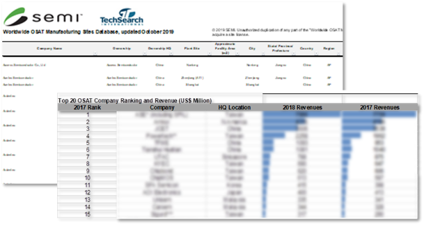
The Worldwide OSAT Manufacturing Sites Database
is a comprehensive report offering insights into global OSAT facilities in China, Taiwan, Korea, Japan, Southeast Asia, Europe and the Americas. The report highlights new and emerging packaging offerings by manufacturing locations and companies. Specific details tracked include:
- Plant site location, technology, and capability: Packaging, Test, and other product specializations, such as sensor, automotive and power devices are highlighted.
- Packaging assembly service offered: BGA, specific leadframe type such as QFP, QFN, SO, flip-chip bumping, WLP, Modules/SIP, and sensors.
- New manufacturing sites announced, planned or under construction.
Tracking advances in packaging technology – which directly affects chip performance, reliability and cost – requires understanding company offerings by location. Key features of the updated report include:
- More than 120 companies and 360 facilities
- More than 200 facilities with test capabilities
- Over 90 facilities offering leadframe CSP
- Over 50 bumping facilities, including 30 with 300mm wafer bumping capacity
- More than 50 facilities offering WLCSP technology
- New facilities offering FOWLP and FOPLP
- More than 100 facilities in China, approximately 100 in Taiwan and 43 in Southeast Asia
The database findings are based on information gathered and compiled from over 120 companies globally. All information in the Worldwide OSAT Manufacturing Sites Database was gathered by SEMI and TechSearch International. Report licenses are available for single-user and multi-users. SEMI members save 16 percent or more depending on the type of license.
For more information about the Worldwide OSAT Manufacturing Sites Database and to order a sample copy, please click here. For pricing and ordering information, please click here.
About SEMI
SEMI® connects more than 2,100 member companies and 1.3 million professionals worldwide to advance the technology and business of electronics design and manufacturing. SEMI members are responsible for the innovations in materials, design, equipment, software, devices, and services that enable smarter, faster, more powerful, and more affordable electronic products. Electronic System Design Alliance (ESD Alliance), FlexTech, the Fab Owners Alliance (FOA) and the MEMS & Sensors Industry Group (MSIG) are SEMI Strategic Association Partners, defined communities within SEMI focused on specific technologies. Visit www.semi.org to learn more, contact one of our worldwide offices, and connect with SEMI on LinkedIn and Twitter.
About TechSearch International, Inc.
Founded in 1987, TechSearch International (Austin, Texas) is a technology licensing and consulting company specializing in accurate, relevant, and timely information on advanced packaging technology and market developments. Visit www.techsearchinc.com.
Association Contacts
Clark Tseng/SEMI
Phone: 886.3.560.1777 ext. 206
Email: [email protected]
Michael Hall/SEMI
Phone: 1.408.943.7988
Email: [email protected]
BRUSSELS, Belgium – November 19, 2019 – SEMI and 19 partners from 14 countries today launched an initiative to fill the skills gap and boost workforce diversity by tightening collaboration between the microelectronics industry and education providers. The project, dubbed METIS – Microelectronics Training, Industry and Skills – will focus on the skills and related training needed to support emerging verticals such as artificial intelligence (AI), autonomous driving and Industry 4.0.

A Sector Skills Alliance co-funded by the Erasmus+ Program, METIS is designed to overcome the skills shortage in the electronic components and systems value chain. Under METIS, SEMI and the partner organizations will establish a Microelectronics Observatory and Skills Council consisting of representatives from industry, academia, NGOs, think tanks and government. The consortium will develop a New Skills Strategy for the microelectronics industry in Europe with a focus on raising occupational profiles and skills critical to the future of the sector.
The project will boost online education and work-based learning in microelectronics design and manufacturing. METIS will also promote workforce diversity in the sector and target increased participation of under-represented groups in microelectronics education and employment. METIS, a four-year project, will receive 4 million EUR in public funding to be invested in microelectronics workforce development in Europe.
The talent shortage is one of the most severe issues challenging SEMI members today,” said Laith Altimime, president of SEMI Europe. “We are excited to partner with leading businesses and universities from across Europe to help build the robust talent pipeline crucial to microelectronics innovation and growth.”
“Digitalization is the key opportunity for the knowledge-oriented economy of our time, in particular for Europe, and semiconductor solutions are key drivers of digitalization,” said Dr. Sabine Herlitschka, CEO of Infineon Technologies Austria AG, a METIS consortium member. “Therefore, microelectronics offers highly attractive job opportunities at the forefront of research and applications relevant to all of us. With this project, we need to convey this enthusiasm for technology to more young talent, in particular women. One effective way of doing so is by tightening the collaboration between the industry and education institutions. This is a strategic core of our new METIS project.”
Sector Skills Alliances work to improve skills intelligence and provide a clear strategy in a target sector through a double-barreled approach of identifying existing or emerging sector-specific labour market needs and enhancing the responsiveness of education and training organizations to industry needs. Sector Skills Alliances are established to facilitate cross-border certification and therefore ease professional mobility and increase recognition of qualifications at European level within a sector.
The METIS consortium consists of SEMI, Infineon, Bosch, X-FAB, Graphenea, Summa, Arcelik, Silicon Saxony, imec, Technical University of Graz, Dresden Chip Academy, University of South-Eastern Norway, Technical University of Sofia, Budapest University of Technology and Economics, IAL-FVG, Fast Track into Information Technology, European Association of Career Guidance, European Association for Women in Science, Engineering and Technology, CIMEA and DECISION.
About SEMI
SEMI® connects more than 2,100 member companies and 1.3 million professionals worldwide to advance the technology and business of electronics design and manufacturing. SEMI members are responsible for the innovations in materials, design, equipment, software, devices, and services that enable smarter, faster, more powerful, and more affordable electronic products. Electronic System Design Alliance (ESD Alliance), FlexTech, the Fab Owners Alliance (FOA) and the MEMS & Sensors Industry Group (MSIG) are SEMI Strategic Association Partners, defined communities within SEMI focused on specific technologies. Visit www.semi.org to learn more, contact one of our worldwide offices, and connect with SEMI on LinkedIn and Twitter.
Association and METIS Contact
Emir Demircan/SEMI Europe
Phone: +32 (0) 2 609 53 18
Email: [email protected]