downloadGroupGroupnoun_press release_995423_000000 copyGroupnoun_Feed_96767_000000Group 19noun_pictures_1817522_000000Member company iconResource item iconStore item iconGroup 19Group 19noun_Photo_2085192_000000 Copynoun_presentation_2096081_000000Group 19Group Copy 7noun_webinar_692730_000000Path
Skip to main content
Default Banner Image

United States

YES (Yield Engineering Systems, Inc. ), a leading manufacturer of process equipment for semiconductor advanced packaging, life sciences and “More-than-Moore” applications, today announced that it has acquired SPEC (Semiconductor Process Equipment Corporation) of Valencia, California for an undisclosed amount. The companies had announced a strategic partnership agreement in June.

The purchase brings together two longtime, trusted semiconductor equipment suppliers with more than 70 years of industry experience between them. “YES and SPEC have many characteristics in common,” said Rama Alapati, CEO of YES. “Both of us have accumulated decades of technological expertise and have installed hundreds of systems in dozens of countries. We both take pride in our many repeat customers, and our excellent industry reputations. In acquiring SPEC, we feel YES is now better-positioned to meet the growing demands of current and future customers in emerging markets such as HPC, AI/ML, 5G, autonomous driving, augmented reality, and other computationally intensive applications.”

“The SPEC product line, which includes cleaning, etching, stripping and plating equipment, complements our portfolio well, and will allow YES to extend our offerings into the wet processing market,” added Rezwan Lateef, President of YES. “We welcome SPEC’s employees to the YES team, and we look forward to developing a variety of new products together to address and anticipate customer needs.”

“SPEC is very pleased to join forces with YES. With global demand for semiconductors increasing dramatically, this merger could not have come at a better time for both companies. We are excited to help YES open new markets and opportunities for our proven wet-process technologies going forward,” said Kevin McGillivray, co-founder of SPEC.

In addition to augmenting its personnel resources with the SPEC staff, YES will gain more than 40,000 square feet of manufacturing, assembly, and cleanroom space in Valencia, as well as SPEC’s regional offices around the world.

About YES
YES (Yield Engineering Systems, Inc.) is a preferred provider of high-tech, cost-effective equipment for transforming surfaces, materials, and interfaces. The company’s product lines include vacuum cure systems, chemical vapor deposition (CVD) systems, and plasma etching tools used for precise surface modification and thin-film coating of semiconductor wafers, semiconductor and MEMS devices, biosensors and medical substrates. With YES, customers ranging from startups to Fortune 100 companies can create and volume-produce products in a wide range of markets, including Advanced Packaging, MEMS, Augmented Reality/Virtual Reality and Life Sciences. YES is headquartered in Fremont, California, with a growing presence globally. For more information, please visit http://www.yieldengineering.com.

About SPEC
SPEC (Semiconductor Process Equipment Corporation) is a highly experienced supplier of surface conditioning wet process equipment. Since 1986, SPEC has designed and manufactured wafer-level and device-level wet process equipment for acid and solvent surface modification (cleaning, etching, stripping), electroplating, and electroless (chemical) plating for all industries requiring a high level of process cleanliness. SPEC’s products are used for polysilicon chip, chunk, and ingot cleaning; crucible cleaning, cavity cleaning for particle accelerators, chemical mixing and delivery, hard drive component cleaning, and quartzware cleaning. SPEC systems are engineered to match the unique requirements of the end user. For more information, please visit http://www.team-spec.com.

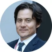
Dr. Anirudh Devgan, President and CEO of Cadence Design Systems, Inc. has been selected to receive the 2021 Phil Kaufman Award for Distinguished Contributions to Electronic System Design.

The Phil Kaufman Award is presented annually by the Electronic System Design Alliance (ESD Alliance), a SEMI Technology Community, and the IEEE Council on Electronic Design Automation (CEDA). The award ceremony and dinner will be held Thursday, March 10, from 6:30pm to 9:30pm at The GlassHouse in San Jose, California. Registration details will be available soon.

Dr. Devgan is being honored for his extensive contributions to electronic design automation (EDA). He is widely recognized as a leading authority in parallel and distributed computing and has made a broad impact in fields ranging from circuit simulation to statistical design and optimization, physical design and signoff, verification and hardware platforms, and system design and analysis. Dr. Devgan's groundbreaking contributions include not just the development of algorithms, but also successfully bringing to market commercial solutions that have gained widespread customer adoption throughout the industry.

"Anirudh has a truly rare combination of widely recognized research excellence, exceptional business impact and results, and outstanding leadership in the EDA industry," said Lip-Bu Tan, former CEO and now Executive Chairman of Cadence, who nominated Dr. Devgan for this honor. "Anirudh's overall contributions during his career spanning Carnegie Mellon, IBM, Magma and Cadence have significantly advanced the industry."

"I have known Anirudh for over 20 years from his early days at IBM and have since closely followed his spectacular career in the industry," said Alberto Sangiovanni Vincentelli, The Edgar L. and Harold H. Buttner Chair of EECS, University of California, Berkeley, a Cadence founder and a Kaufmann Award winner. "I know of hardly anyone in EDA who has that winning combination of bold vision and deep technical know-how, along with outstanding leadership and organizational skills. Leveraging these unique abilities, Anirudh has been able to constantly innovate in a mature field like EDA and bring to market a sequence of game-changing products that have delivered transformational business results."

"On behalf of the ESD Alliance, I would like to congratulate Anirudh on receiving the 2021 Phil Kaufman award," said Simon Segars, ESD Alliance Chairman and CEO of Arm Holdings. "His contributions in technical innovation have been foundational to bringing the EDA industry into the modern parallel and cloud computing era. Anirudh's impact on the industry is well-recognized and celebrated with this distinguished honor."

About Dr. Anirudh Devgan, the 2021 Phil Kaufman Award Recipient
Dr. Devgan joined Cadence in 2012, has served as President of Cadence since 2017 and has been a member of the Cadence Board of Directors since August 2021. He assumed the additional role of Cadence CEO on December 15, 2021.

Dr. Devgan began his career at the IBM Research (Thomas J. Watson Research Center) in 1994. His work at IBM on EDA algorithms and design optimization techniques contributed to IBM's leadership in the 1990s and 2000s in high-performance microprocessor and server designs. He joined Magma Design Automation in 2005 as a key member of its Executive Management Team and General Manager of the Custom Design Business Unit. He initiated and brought to market multiple new products in the areas of circuit simulation, analog mixed-signal design, physical verification, library characterization and 3D extraction among others. The products were successful in both customer adoption and business results.

At Cadence, Dr. Devgan has spearheaded technology excellence and driven the re-architecture and revamping of its product lines, notably the entire suite of digital and signoff tools, as well as its functional and mixed-signal simulation solutions. Dr. Devgan established Cadence's Intelligent System Design strategy and is driving breakthrough advancements in cloud, artificial intelligence (AI) and machine learning (ML) and system innovation. Dr Devgan's leadership and contributions have had a transformational impact, with a significant increase in Cadence's revenue, profitability and market capitalization as well as in the overall customer and market adoption of its solutions.

Dr. Devgan has received best paper awards from both leading conferences in the field – Design Automation Conference (DAC) and International Conference on Computer Aided Design (ICCAD). Dr. Devgan is an IEEE Fellow, holds 27 U.S. patents and has published numerous research papers in leading journals and conferences. Dr. Devgan received a Bachelor of Technology degree in Electrical Engineering from the Indian Institute of Technology, Delhi, and Master of Science and Ph.D. degrees in Electrical and Computer Engineering from Carnegie Mellon University.

About the Phil Kaufman Award
The Phil Kaufman Award honors individuals who have had a demonstrable impact on the field of electronic system design through technology innovations, education/mentoring, or business or industry leadership. The award was established as a tribute to Phil Kaufman, the late industry pioneer who turned innovative technologies into commercial businesses that have benefited electronic designers. The 2019 recipient was Dr. Mary Jane Irwin, Evan Pugh Professor and A. Robert Noll Chair Emeritus in Engineering in the Department of Computer Science and Engineering at Pennsylvania State University. Due to the COVID-19 pandemic, there was no Phil Kaufman Award in 2020.

About the IEEE Council on Electronic Design Automation (CEDA)
The IEEE Council on Electronic Design Automation (CEDA) provides a focal point for EDA activities spread across seven IEEE societies (Antennas and Propagation, Circuits and Systems, Computer, Electron Devices, Electronics Packaging, Microwave Theory and Techniques, and Solid-State Circuits). The Council sponsors or co-sponsors over a dozen key EDA conferences including: the Design Automation Conference (DAC), Asia and South Pacific Design Automation Conference (ASP-DAC), International Conference on Computer-Aided Design (ICCAD), Design Automation and Test in Europe (DATE), and events at Embedded Systems Week (ESWEEK). The Council also publishes IEEE Transactions on Computer-Aided Design of Integrated Circuits & Systems (TCAD), IEEE Design & Test (D&T), and IEEE Embedded Systems Letters (ESL). The Council boasts a prestigious awards program in order to promote the recognition of leading EDA professionals, which includes the A. Richard Newton, Phil Kaufman, and Ernest S. Kuh Early Career Awards. The Council welcomes new volunteers and local chapters.

Stay in touch with IEEE CEDA:

Website: www.ieee-ceda.org
LinkedIn: https://www.linkedin.com/groups/8343531
Facebook: https://www.facebook.com/ieeeceda/
Twitter: https://twitter.com/IEEECEDA

About the Electronic System Design Alliance
The Electronic System Design (ESD) Alliance, a SEMI Technology Community representing members in the electronic system and semiconductor design ecosystem, addresses technical, marketing, economic and legislative issues affecting the entire industry. It acts as the central voice to communicate and promote the value of the semiconductor design ecosystem as a vital component of the global electronics industry. Visit www.semi.org/en/communities/esda to learn more.

Follow the ESD Alliance:

ESD Alliance Bridging the Frontier blog
Twitter: @ESDAlliance
LinkedIn
Facebook

About SEMI
SEMI® connects more than 2,400 member companies and 1.3 million professionals worldwide to advance the technology and business of electronics design and manufacturing. SEMI members are responsible for the innovations in materials, design, equipment, software, devices, and services that enable smarter, faster, more powerful, and more affordable electronic products. Electronic System Design Alliance (ESD Alliance), FlexTech, the Fab Owners Alliance (FOA) and the MEMS & Sensors Industry Group (MSIG) are SEMI Strategic Technology Communities, defined communities within SEMI focused on specific technologies. Visit www.semi.org to learn more, contact one of our worldwide offices, and connect with SEMI on LinkedIn and Twitter.

Lanza techVentures, an early-stage investment firm that supports entrepreneurs to realize their innovative, new ideas in technologies, products and business models, is tapping the semiconductor industry expertise of Rick Carlson, naming him its newest investment partner.

In this role, Carlson will work closely with Lucio Lanza, managing partner of Lanza techVentures, and other investment partners to identify new and emerging markets and entrepreneurial startups in need of early-stage capitalization. Current interests include the intersection of semiconductors and medical technology, and intelligence at the edge.

“Rick is an enthusiastic and intuitive investor and I’m delighted he is a Lanza techVentures investment partner,” remarks Lucio Lanza, Lanza techVentures’ managing partner. “His in-depth knowledge of the semiconductor market will help ensure sound investment strategies.”

“Lucio has a unique ability to triangulate multiple disparate events to arrive at breakthrough insights that are not obvious,” notes Carlson. “His experience and wisdom have shown up in the successful outcomes of many Silicon Valley enterprises. I’m pleased to have the opportunity to be part of Lanza techVentures.”

Currently, Carlson is an active seed investor and serves as vice president of sales at Verific, often acting as an advisor to various electronic design automation (EDA) startups. He has been in the EDA industry since 1980 and has held sales and sales management positions with Calma, Mentor Graphics (now Siemens), Daisy Systems, EDA Systems, Escalade, Synplicity and AccelChip. Carlson co-founded the EDA Consortium (now the ESD Alliance, an industry trade association) and initiated the drive that led to the Phil Kaufman Award for Distinguished Contributions to Electronic System Design, EDA’s most prestigious award. He took a hiatus from EDA to help launch the FLEXlm product for license management at Highland Software (now Flexera Software). Carlson received a Bachelor of Science degree in Mathematics from the Illinois Institute of Technology in Chicago.

About Lanza techVentures
Lanza techVentures is an early-stage investment firm that transforms innovative startups into high-value companies through unique vision, insight and a profound understanding of technology and its trends. Founded in 2001 by technology luminary Lucio Lanza, Lanza techVentures has acted as a strategic partner and advisor for early- to mid-stage companies in the design software and intellectual property (IP), semiconductor and biotechnology market sectors.

Follow Lanza techVentures at:
Website: http://lanzatechventures.com/
Twitter: @LTechventures
LinkedIn: https://bit.ly/3CFKlxn

ESPOO, Finland, 14th of December 2021 - There has been a need for enhanced coating methods in organic electronic manufacturing as foldable phones and other future product iterations need materials that are lighter, more reliable and enable folding and stretching of a device. Thus, the use of thin film encapsulation solutions has become more common in organic electronic manufacturing.

Atomic layer deposition (ALD) has already proven to be the coating solution of choice for a wide range of applications in the semiconductor industry. Inorganic films, which are the standard output of an ALD process, are however susceptible to crack or develop defects under severe mechanical stress. This issue is magnified when depositing on large surface areas often required in flexible organic electronics manufacturing. Picosun’s novel approach to address these issues, for which patent rights are pending, includes nanolamination of dense inorganic layers deposited with ALD to maintain excellent barrier performance‚ with organic or hybrid molecular layer deposition (MLD) layers to offer enhanced flexibility and de-emphasize the defects which may appear when films are stressed.

Picosun research on an industrially viable ALD/MLD process was demonstrated on wafers and polymer substrates over 200 mm in diameter with a deposition temperature of 90 °C using Picosun ALD tools. The results showed great thickness uniformity and higher throughput compared to pure ALD film deposition. The MLD film proved to be stable in ambient environment and the complementary strengths of ALD and MLD hindered H2O permeation through the film stack, which enables flexibility in moisture barrier design.

“We are excited to bring these insights to the market as there has been little information available from stable and industrially viable MLD processes in full wafer scale. Besides organic electronics, we see immense potential with the ALD/MLD films in the manufacturing of LEDs, MEMS and medical packaging”, states Juhana Kostamo, VP, Industrial Business Area of Picosun Group.

Watch the Picosun webinar to learn more about the topic and Picosun results:
https://info.picosun.com/webinars/ald-mld-nanolaminate-films

More information:
Juhana Kostamo
Vice President, Industrial Business Area, Picosun Group
Tel: +358 50 369 9565
Email: [email protected]
www.picosun.com

About Picosun
Picosun provides the most advanced ALD (Atomic Layer Deposition) thin film coating solutions for global industries. Picosun’s ALD solutions enable technological leap into the future, with turn-key production processes and unmatched, pioneering expertise in the field – dating back to the invention of the technology itself. Today, PICOSUN® ALD equipment are in daily manufacturing use in numerous leading industries around the world. Picosun is based in Finland, with subsidiaries in Germany, USA, Singapore, Japan, South Korea, China mainland and Taiwan, offices in India and France, and a world-wide sales and support network. Visit www.picosun.com.

August 30, 2021 11:30 AM SAST

AMSTERDAM–Leading AI-for-Manufacturing company, DataProphet, today announces the formation of its Semiconductor Advisory Board. With great pride, the company welcomes the newly formed strategic committee of trusted industry-specific advisors — Susan Wilkerson and Markus Keil.

In Markus Keil and Susan Wilkerson, DataProphet has teamed with two highly respected, seasoned professionals who are deeply committed to bringing their wealth of semiconductor industry knowledge to help DataProphet achieve its ambitions of integrating its data-driven AI-as-a-Service into all value-adding processes in the semiconductor value chain around the world, including fabs and Original Equipment Manufacturers (OEMs).

Susan Wilkerson and Markus Keil are distinguished additions to DataProphet’s wider Industry Advisory Board. They directly reflect the company’s growth-oriented, go-to-market mindset at a crucial inflection point in its commercial development.

DataProphet’s Semiconductor Advisory Board members bring a proven track record as change agents in semiconductor manufacturing, helping shape and guide the industry through myriad challenges and transformations over years of unprecedented technological and economic transformation. Susan Wilkerson and Markus Keil will work closely with DataProphet’s leadership team to ensure they are best meeting the critical production KPIs of the semiconductor industry as it moves into a new era.

Regarding the announcement, Susan Wilkerson had this to say: “I’m excited to be selected for DataProphet’s Semi Advisory Board, which focuses on utilizing AI and Machine Learning to enable prescriptive operational efficiencies in the Semiconductor industry. The Dataprophet team’s underlying philosophy translates into product offerings committed to making the end customer experience as simple and positive as possible while proving clear customer value at every stage. Their AI-as-a-Service seamlessly inputs environmental variables and proactively models complex integration in the manufacturing process. This will enable chipmakers to address their most significant technical challenges. With DataProphet’s data-driven solutions, fabs will access opportunities to improve operational cost, yield, and time to market faster than ever before.”

Markus Keil contextualized the significance of his inclusion in this way: “Upon meeting the DataProphet team, I became quickly aware of a unique group of excellent talents and leadership backed by high-caliber investors. My sense was: here is a company to make a big difference in the young industry of AI. This is why I’m very honored to have the opportunity to support DataProphet in bringing its AI-for-Manufacturing and Machine Learning (ML) applications into the semiconductor industry. AI and ML are megatrends with the capability to influence many aspects of how we work, design, build and use technology. Furthermore, in my opinion, semiconductors are a logical and natural target industry for DataProphet’s pioneering technology. Fabs are very data-centric environments with some catch-up work to do in using AI. With Dataprophet’s unique innovations, its use of big data prescriptive analytics, along with their very customer-centered approach, I am convinced this company will be successful in bringing its game-changing technology to fabs worldwide.”

In response to the formation of the Advisory Board, DataProphet CEO and co-founder Frans Cronje stated: “I am very excited by today’s announcement of our Advisory Board for the semiconductor industry! The experts who have joined our board will help guide DataProphet as we introduce our state-of-art AI solution to fabs around the world. Susan Wilkerson and Markus Keil will help us navigate the intricacies and challenges that customers in the semiconductor manufacturing industry face. I am looking forward to the results we will achieve together.”

ABOUT DATAPROPHET
DataProphet is a Venture Capital-backed, high-growth AI-for-Manufacturing company pioneering the development and deployment of Deep Learning solutions for manufacturers across key industry verticals worldwide. As heavy industries move towards autonomous manufacturing, its world-leading AI-driven solutions guide clients from over-dependence on human experts to Machine Learning expert guidance. DataProphet’s mission is for its manufacturing process agnostic AI-as-a-Service innovations to continue revolutionizing process optimization in support of the wide range of manufacturing sectors it currently partners with and to extend its partnerships even further. The company helps manufacturers—of semiconductors, automotive equipment, rubber, glass, plastic, gray iron, and minerals—meet and exceed critical KPIs with cutting-edge, human-in-the-loop AI deployments requiring no additional hardware investment. In this way, DataProphet supports adopters of its technology to become more competitive and resource-efficient as they digitally transform. DataProphet AI deployments guarantee ROI in the first year of operation and provide ongoing and complete post-installation support, including additional data sources and full model maintenance.

ABOUT SUSAN WILKERSON
Susan Wilkerson joined Veeco in April 2020 as Senior Vice President of Global Customer Operations. Before her employment with Veeco, she served as Vice President & General Manager of Strategic Global Accounts for Lam Research Corporation from 2011 to 2020. She was also previously Vice President & General Manager of Americas Sales & Service for Verigy. Susan Wilkerson was with Applied Materials for over fifteen years, holding positions of increasing responsibility—these included Global Account Management, Vice President & General Manager, and Vice President of Operations for the North America Region. Susan Wilkerson was also engaged in multiple consulting ventures, co-founding BlueRock Consulting LLC in 2008.

ABOUT MARKUS KEIL
Markus Keil has 25 years of global experience in the technology industry with a strong operational and business focus in Asia, Europe, and the US. Mr. Keil has worked as a CEO, Business Area Manager, and Business Unit COO in highly innovative environments. He also bore Multi-Operations-Site responsibility for ten manufacturing sites in six countries (in Europe, the US, and Asia), and brings solid operational experience along the entire semiconductor manufacturing supply chain—from Equipment Vending, Wafer Manufacturing, Chip-Packaging, Multi-Chip Module Assembly, and Testing with a large inhouse and outsourced footprint. Mr. Keil started up several manufacturing sites (greenfields), transferring technology and building HVM Technology organizations. He has post-M&A integration experience and has led several significant organizational integration and transformation projects in the semiconductor industry. Markus Keil is a hands-on team player and vision builder with a strategic mindset.

The two leaders announced a partnership that includes a new JEOL demonstration facility located in Covalent’s Silicon Valley lab. The partnership will accelerate applications development and broaden client access to a suite of state-of-art instrumentation and analytical services.

December 07, 2021 – Sunnyvale, CA. Covalent Metrology, a leading North American provider of analytical services, announces its partnership with JEOL a global leader in the development of cutting-edge scientific instruments used in microscopy, analytical chemistry, and materials characterization. JEOL’s state-of-art metrology instruments spanning these disciplines are coming soon to the announced JEOL USA demonstration facility, located within Covalent’s Silicon Valley lab.

Covalent works with scientists and engineers from more than thirty industries, including semiconductor, battery and energy storage, electronics, and medical devices. The new demonstration facility will receive JEOL’s top-of-line electron microscopes and spectrometers over the coming months and will soon benefit clients across these sectors.

The partnership deepens JEOL’s presence in Silicon Valley and will expand Covalent’s capacity and capabilities offered. The demonstration facility will serve as a platform to research and highlight technologies and methods tailored for advanced material and device analysis. JEOL will work closely with Covalent’s team of experts to deepen understanding of the market’s analytical needs - informing JEOL’s development of next generation hardware, software, and applications research.

The Covalent and JEOL USA partnership delivers on their commitment to providing market access to advanced learning opportunities, and access to expertise and firsthand experience with cutting-edge instrumentation. The partners will host a variety of demonstrations and educational events at the lab’s demonstration facility. JEOL’s commitment to providing Covalent experts access to the company’s newest instruments, ensures Covalent customers benefit from the most advanced instrumentation available.

Craig Hunter, Covalent Founder and CEO, commented, “JEOL has been a pioneer and leader in analytical instrumentation for 70 years. Their products are enabling some of the most exciting science and engineering happening around the world right now – work that is revolutionizing so many aspects of our modern society. We are honored that JEOL has chosen to partner in such a meaningful way with Covalent, and we are thrilled to house their Silicon Valley and West Coast demonstration lab here in Sunnyvale.”

Robert Pohorenec, President of JEOL USA, stated, “Covalent Metrology provides world-class expertise to a very diverse set of industries in order to solve very complex problems. They and their clients require state-of-the-art metrology and analytical instrumentation. Partnering with Covalent Metrology is an exciting opportunity for JEOL to expand awareness of JEOL’s technology in the industries served by Covalent and it will provide us deeper insight into the needs of researchers and industries that both our organizations desire to serve.”

For Media inquiries regarding Covalent Metrology please contact:
Shannon Scheiwiller, Chief Marketing Officer, [email protected]

About Covalent Metrology
Covalent Metrology is a disruptive analytical services laboratory and platform based in Sunnyvale, California. Its mission is to help companies who use advanced materials to get better data and insights more easily and affordably to facilitate faster development and production. Covalent is dramatically changing the characterization and imaging landscape by combining transparent pricing, data platforms, and top-notch customer service with world-class scientists, state-of-art tools, and strategic partnerships.
Covalent now has over 500 customers in 30+ industries.
Learn more at: https://covalentmetrology.com

About JEOL
Since 1949, the JEOL legacy has been one of outstanding innovation in developing instruments used to advance scientific research and technology. JEOL has more than 70 years of expertise in the field of electron microscopy, more than 60 years in mass spectrometry and NMR spectrometry, and more than 50 years of e-beam lithography leadership.
JEOL USA, Inc., a wholly-owned subsidiary of JEOL Ltd. Japan, was incorporated in the United States in 1962. The primary business of JEOL USA is sales of new instruments and peripherals and support of a vast installed base of instruments throughout the United States, Canada, Mexico, and South America.

Learn more at www.jeolusa.com

Boron-Free Nickel Plating for Semiconductor Applications

Cranston, RI, USA – Technic is pleased to announce the commercial release of Elevate Ni 5950, after several successful production installations. The process has been run successfully in a variety of applications including pattern plating, metal stack plating, and as a hard mask for difficult to etch substrates such as SiC.

Unlike the current standard boric acid nickel processes, Elevate Ni 5950 utilizes all liquid components, making it easier to replenish and more compatible with semiconductor fabrication processes.

"Nickel electroplating chemistries with boric acid have been utilized for decades in the electronic and industrial plating industries. The replacement of boric acid could only be successful if the nickel deposit was uncompromised. Elevate Ni 5950 has been shown to not only produce deposits that are comparable to standard nickel plating processes, but in many cases, the deposit attributes have shown superior results."

- Anthony Gallegos, Global Product Manager, Semiconductor Technology

About Technic, Inc.
Technic continues to be a leader in the development of specialty chemicals for the semiconductor industry that are free of toxic components and safer for the environment. Technic sulfite gold chemistries are free of toxic additives like thallium and arsenic and our NMP free photoresist strippers, are just a few examples of products currently being used around the world in mass production enabling safer and more sustainable production.

Learn More: https://www.technic.com/applications/semiconductor/fabrication-packagin…

November 03, 2021 | 11:30 AM SAST | Nicol Ritchie | • Press releases

AMSTERDAM - DataProphet, the leading AI-for-manufacturing company, today announced the extension of its Semiconductor Advisory Board. The award-winning industrial technology business welcomes Dr. Antonio (Toni) Mesquida Küsters. Dr. Mesquida Küsters joins Susan Wilkerson and Markus Keil, who recently formed this strategic committee of specialist semiconductor advisors at DataProphet in August of 2021.

Toni brings more than 25 years of management experience in the semiconductor industry, where he has held positions at major integrated circuit and semiconductor equipment manufacturers such as Infineon and ASML, where he currently heads up product marketing and business development. His responsibilities have included product marketing, business development, strategy and sourcing & operations management.

As an experienced venture capital investor, Mesquida Küsters also understands start-ups, how they operate and how they best execute expansion strategies. This experience will be relevant as DataProphet extends a global presence in the silicon space via its broader Integrator and Machine Builder partnership ecosystem.

Taken together, DataProphet's Semiconductor Advisory Board members bring a wealth of frontline semiconductor experience. Furthermore, Dr. Toni Mesquida Küsters, Susan Wilkerson and Markus Keil are outstanding additions to the broader DataProphet Industry Advisory Board, which will increasingly bolster the business’s expansion strategy as this relates to the diverse and critical manufacturing verticals benefiting from its AI-as-a-Service.

Specifically, the Semiconductor Industry Advisory board will work closely with DataProphet's leadership team as they strive to revolutionize production for the semiconductor industry worldwide with advanced Deep Learning.

The inclusion of Dr. Mesquida Küsters to the DataProphet team directly reflects the business's growth-oriented, go-to-market mindset at a crucial turning point in its commercial development.

Speaking of the announcement, Toni Mesquida Küsters had this to say:

"I am delighted to join the DataProphet team and contribute with my network and expertise to the growth of this exceptional company. As widely covered in the news, especially since the COVID pandemic started, semiconductor chips have become one of the key bottlenecks in many supply chains, including automotive, industrial, and consumer, to name a few. There is huge pressure from OEMs towards chip makers to increase the output of their factories by improving their yield and efficiency. Here is where manufacturing solutions based on Artificial Intelligence will bring huge value, as provided by DataProphet. The value of AI will be especially significant for IC makers, who barely use it in their current operations. I'm looking forward to working with Susan and Markus and the DataProphet management team in making the expansion of the company into the Semiconductor market a great success."

In response to the expansion of the Advisory Board, Frans Cronje, CEO, and Co-Founder of DataProphet stated:

"I'm thrilled to welcome Toni to our Semiconductor Advisory Board. Along with Susan Wilkerson's and Markus Keil's, Dr. Mesquida Küsters expertise will help us overcome the complex challenges customers contend with during semiconductor manufacturing. I look forward to the results we will achieve together as we roll out DataProphet's state-of-the-art AI technology for chipmakers and semiconductor machine builders."

ABOUT DATAPROPHET
DataProphet is a venture-backed, high-growth AI for manufacturing company that pioneered the development and delivery of Deep Learning solutions for manufacturers in key industries worldwide. As heavy industry moves towards autonomous manufacturing, its world-leading AI-powered solutions move customers from over-reliance on human experts to machine learning expert guidance. DataProphet's mission is for its manufacturing process-agnostic AI-as-a-Service innovations to continue revolutionizing process optimization—supporting its manifold manufacturing sector partners while expanding these partnerships globally.

DataProphet helps manufacturers of semiconductors, automotive equipment, rubber, glass, plastics, cast iron, and minerals to meet and exceed critical KPIs with cutting-edge AI-as-a-Service. Requiring no additional hardware investments, DataProphet supports users of its technology to become more competitive and more resource-efficient at any stage of the digital transformation journey. DataProphet AI deployments guarantee ROI in the first year of operation and provide ongoing and complete support after installation—including additional data sources and full model maintenance.

ABOUT TONI MESQUIDA KÜSTERS
Dr. Antonio (Toni) Mesquida Küsters joined ASML in Veldhoven as Director of Market Intelligence in 2006, where he significantly contributed to the management directions and priorities of the Dutch company. Between 2011 and 2014, he served as Sourcing Director and Managing Director of the ASML German Operations in Alsdorf (formerly Ushio / Xtreme Technologies) in EUV DPP Sources. Since the beginning of 2015, Toni has been in charge of product marketing & business development for all TWINSCAN dry lithography products with yearly sales of close to 2 billion Euros.

Between 1995 and 2001 in Munich, Toni held various management positions at Siemens AG (later Infineon Technologies AG) in IC development, technology transfer, product marketing, and corporate venturing. As one of the founding members of Infineon Ventures, he served on the supervisory board of various high-tech start-ups worldwide. At the German MOCVD equipment provider, AIXTRON SE, he was head of Corporate Strategy between 2002 and 2006.

Toni holds both Spanish and German nationality and earned his master's degree in Electrical Engineering (1990). He also attained a Ph.D. in Semiconductor Science (1994) from the RWTH Aachen in Germany. His technical education has been extended over the last 25 years with various executive courses at well-known business schools like INSEAD and Rotterdam School of Management.

Breker Verification Systems today unveiled its System Coherency Synthesis TrekApp used to generate thousands of high-coverage tests to stress cross-system coherency for a broad range of SoC platforms and processors.

Based on Breker’s Cache Coherency TrekApp, the System Coherency Synthesis TrekApp uses abstract models of common and novel algorithms to automatically generate coherency test content for complex, multi-agent system platforms based on coverage directives. The TrekApp can be configured for Arm, RISC-V and other processor configurations and broad range of storage and I/O architectures.
“System coherency is an increasingly complex and error-prone challenge for many SoC platforms that requires considerable expertise and effort to accomplish,” says Adnan Hamid Breker’s executive president and CTO. “Our Test Suite Synthesis technology produces dramatic improvements in test composition time and coverage over manual tests and basic test generators including templating schemes.”

Breker, the leading provider of advanced test content synthesis solutions for SoC, UVM and Post-Silicon verification environments, will demonstrate its System Coherency Synthesis TrekApp and other solutions at Design Automation Conference (DAC) in Booth #2528. DAC will be held Monday, December 6, through Wednesday, December 8, from 10 a.m. until 6 p.m. at Moscone West in San Francisco.

Introducing the System Coherency Synthesis TrekApp
The increase in SoC complexity and diverse processor architectures makes coherency a challenge that cannot be ignored in semiconductor development projects. Breker’s next-generation TrekApp uses its Test Suite Synthesis technology to address coherency across the entire system to include fabric and I/O issues as well as advanced memory architectures more effectively than zero abstraction templating and similar schemes.

The TrekApp leverages established methods such as the Dekker algorithm, the Moesi state protocol for system-wide testing, stride testing, false sharing analysis and other exclusive test mechanisms.
Coupled with a range of processor integration tests for Arm v8/v9 and the RISC-V Instruction Set Architecture (ISA) the TrekApp generates comprehensive test content for most SoCs in development today. Specialized custom instructions or even complete instruction sets can be included, and alternative test algorithms can be inserted, crossing test content output results for high verification coverage.

The System Coherency TrekApp generates C code and transactions for system-level testbenches or UVM sequences for cache unit and sub-system simulation. It operates on virtual prototype platforms, simulation, emulation, FPGA prototyping or final silicon, and enables the full debug and profiling of the device under test on those platforms.

The System Coherency Synthesis TrekApp is a component of the Breker TrekApp solution library that provides automated test content for a variety of SoC scenarios, including cache coherency, Arm and RISC-V integration, power domain management, security and network traffic generation. TrekApps operate on the Breker Test Suite Synthesis Solution and Synthesizable VerificationOS for automated, coverage-driven test generation for a variety of multi-threaded platforms from a single, easy-to-understand specification model.

Availability and Pricing
System Coherency Synthesis TrekApp is available and in use on multiple development projects.
Pricing is available upon request.
For more information, email [email protected].

About Breker Verification Systems
Breker Verification Systems is a leading provider of Portable Stimulus solutions, a standard means to specify verification intent and behaviors reusable across target platforms. It is the first company to introduce graph-based verification and the synthesis of powerful test sets from intent-based, abstract scenario models based on AI planning algorithms. Breker’s Test Suite Synthesis and TrekApp library allows the automated generation of high-coverage, powerful test cases for deployment into a variety of UVM, SoC and Post-Silicon verification environments. Case studies that feature Altera (now Intel), Analog Devices, Broadcom, IBM, Huawei and other companies leveraging Breker’s solutions are available on the Breker website. Breker is privately held and works with leading semiconductor companies worldwide.

Engage with Breker at:
Website: www.brekersystems.com
Twitter: @BrekerSystems
LinkedIn: https://www.linkedin.com/company/breker-verification-systems/
Facebook: https://www.facebook.com/BrekerSystems/

TrekSoC, TrekSoC-Si, TrekBox and SoC Scenario Modeling are registered trademark of Breker Verification Systems. Breker Verification Systems acknowledges trademarks or registered trademarks of other organizations for their respective products.

San Francisco, California–December 7, 2021– Brewer Science, Inc., a global leader in developing and manufacturing next-generation materials and processes for the microelectronics and optoelectronics industries, will be presenting its trailblazing efforts as a Certified B Corporation™ at the SEMICON West annual conference in hopes to inspire a more sustainable and inclusive industry.

In May 2021, Brewer Science became the first Certified B Corporation in the semiconductor industry. The certification accredits the company for meeting the “highest standards of corporate social and environmental performance, transparency, and accountability to all their stakeholders.” An extensive audit evaluates all facets of the company, determining areas for improvement in the scope of five Impact Areas: Governance, Workers, Community, Environment, and Customers.

“Brewer Science was founded on the philosophy that directly aligns with the B Corp purpose of ‘using business as a force for good.’ We have programs in place that exemplify our commitment to our people, our customers, and the community. By sharing and collaborating with our supply chain counterparts, together we can create a more sustainable and inclusive industry,” states Matthew Beard, Executive Director of Strategic Planning, Management Systems, and Sustainability at Brewer Science.

Matthew Beard will be presenting at the SEMICON West conference with a talk titled, “Attracting and Retaining the Best Talent and the Purpose Driven Organization.”

The 2021 SEMICON West conference is held December 7th thru 9th at the Moscone Center in San Francisco, California. The conference unites the entire extended electronics supply chain, with the mission “to see what’s next and discover the latest innovations driving industry growth.” Brewer Science is hosting a presentation at the event to encourage other tech innovators to consider B Corp certification for their companies to pave a pathway for continuous improvement within the industry.

You can learn more about Brewer Science by visiting their website: www.brewerscience.com, or schedule a meeting with an expert by emailing, [email protected].

About Brewer Science
Brewer Science is a global leader in developing and manufacturing next-generation materials and processes that foster the technology needed for tomorrow. Since 1981, we’ve expanded our technology portfolio within advanced lithography, advanced packaging, printed electronics, and smart devices to enable cutting-edge microdevices and unique monitoring systems for industrial, environmental, and air applications. Our relationship-focused approach provides outcomes that facilitate and deliver critical information. Our headquarters are in Rolla, Missouri, with customer support throughout the world. We invite you to learn more about Brewer Science at www.brewerscience.com.

###

Company Contact:

Tracy Jenkins
Tel: (US) +1.573.364.0300, ext. 1427
Email: [email protected]