downloadGroupGroupnoun_press release_995423_000000 copyGroupnoun_Feed_96767_000000Group 19noun_pictures_1817522_000000Member company iconResource item iconStore item iconGroup 19Group 19noun_Photo_2085192_000000 Copynoun_presentation_2096081_000000Group 19Group Copy 7noun_webinar_692730_000000Path
Skip to main content
On March 1, the semiconductor industry lost a true legend with the passing of Bill Tobey, an exemplary leader and contributor to the semiconductor industry throughout his career. SEMI honored Bill with our Bob Graham Sales and Marketing Excellence Award in 2006 for his work on wafer steppers. Bill and his team had the foresight to recognize that competing solutions such as Deep Ultraviolet (DUV) projection, e-beam, and x-ray would not be able to keep up with Moore’s Law. More importantly, Bill had the passion and marketing prowess to convince customers of this, even though early wafer steppers were twice as expensive and considerably slower than the alternatives. He used that passion to also convince management at GCA Corporation that they needed to shift resources to advance steppers and drive alignment with customers. I remember the critical role he played when we worked with GCA steppers during my early years at AT T Bell Labs. The Chip History Center virtual museum has a wonderful video interview with Bill Tobey on his conceptualizing of the wafer stepper and on his winning of the Bob Graham Award. Dan Hutcheson, CEO and chairman of VLSIresearch, shared these kind words on Bill Tobey’s influence: “The world of semiconductors and the products they made possible would have been much smaller, as Moore's Law might have stopped at 2 microns, without Bill's contributions. His ability to see what others could not probably explains why he was able to continue making contributions into his nineties. Companies all over the world continued to call on him to his last days.” Bill’s contributions were limitless. He was a member of the organizing committee for the SEMI Industry Strategy Symposium (ISS) and chaired it in its early years. After completing his term serving ISS, he joined the committee for the SEMI International Trade Partners Conference (ITPC). Bill also served as a member of the SEMI East Coast advisory committee in its early years and was responsible for industry meetings in the area. And he was involved with many other SEMI activities on behalf of the industry. Bill's obituary is posted on the funeral home website. For all of us working in the semiconductor industry, we are honoring Bill Tobey’s memory by continuing to build upon the foundation that he helped to establish. I hope you are inspired by the passion he displayed in his work throughout his career and encourage those who knew him to share stories of Bill to further inspire others to follow the example he set. Ajit Manocha is president and CEO of SEMI.
Read More
The work of the SEMI Environment, Health and Safety (EHS) COVID-19 working group to address industry EHS issues and share best practices has morphed as rapidly as COVID-19 itself as the vaccine rollout continues, inspiring new hope for a return to normal. The group has evolved from mounting crisis responses to urgent issues such as the shortage of masks and sanitization wipes and sprays to helping companies prepare for their employees’ return to the workplace and developing on-site health-screening procedures for employees and visitors to help ensure their safety. Hot SEMI EHS COVID-19 working group topics have included the following as the team continues to meet every other week to stay abreast of COVID-19 developments and their industry impacts. Vaccinations SEMI members have been monitoring the progress of U.S. states and counties in delivering vaccines. So far, no essential workers in the electronics industry have been eligible to be vaccinated. To help gauge the availability of vaccines to essential industry workers, some companies have hired external consultants to monitor the phase-in. The SEMI EHS COVID-19 working group will collect and centralize the information to help members plan for their employees’ return to the workplace. Policy Enforcement At manufacturing sites, some employees reportedly are becoming complacent in following masking and distancing policies, prompting reminder communications from top management for workers to comply until the pandemic is brought to heel. The higher-ups are also encouraging staff to get vaccinated once they are eligible, with some member companies offering workers time off or other incentives for their employees and families to get vaccinated. Contact Tracing Despite the intense focus on contact tracing since the initial COVID-19 outbreak last year and early efforts to track people movement using smartphone applications or wearables, no tracking technology has emerged as the standard for helping to curb the virus’s spread. SEMI members have been testing various technologies ranging from Bluetooth to wearables with wide-band radio waves to track employees while on site. Tracing by wearables has proven inaccurate. Left with no better alternative, the vast majority of SEMI members are performing time-consuming manual contact tracing. OSHA Compliance While OSHA has picked up the pace in issuing new regulations related COVID-19, pandemic-related site inspections have lagged, some SEMI working group members report. In California, CAL/OSHA recently passed a COVID-19 Preparedness Plan that defines the responsibility of employers in preventing workplace outbreaks, offering PPE to workers and conducting frequent testing. The California plan mirrors the CDC recommendations implemented at the onset of the pandemic. To join the SEMI EHS COVID-19 working group, contact our EHS team at [email protected]. Olivier Corvez is senior manager of Environment, Health, Safety and Sustainability at SEMI.
Read More
The automotive industry is changing. Our vehicles are getting electrified, connected and automated. As this trend is accelerating, it’s having an impact on how semiconductor devices, including MEMS sensors, are designed and qualified for automotive. As automotive semiconductor designers carefully consider product definition, product validation, and long-term reliability, MEMS sensor suppliers are responding to new opportunities created by electrified and automated vehicles by developing inertial measurement units (IMUs) for automated driving as well as battery pressure monitoring sensors for Li-ion EV batteries. The most complex MEMS device of all The automotive MEMS IMU is probably the most complex MEMS device that will be used inside a vehicle. This type of IMU is a System-in-Package (SiP) comprised of multiple gyroscope and accelerometer sensing elements plus a signal processing ASIC, integrated into one package that creates an inertial sensor able to measure up to six degrees of freedom (6DoF): yaw, roll and pitch for rotational movements, and lateral, longitudinal and vertical acceleration for linear movements. Degrees of freedom in a vehicle For vehicles with Level 3 autonomy and above (per SAE definition), the IMU is mandatory for taking over the trajectory control of the vehicle in case other sensors, such as the camera, radar or LiDAR, become impaired. Should such a failure occur, the IMU will function as a guidance sensor to bring the car to a safe stop within a short period of time and distance. The IMU is also used to control the regular movement of the car while driving in automated mode. While IMU technology already exists for aerospace applications, there are significant challenges to adapting it for automotive. The automotive IMU requires high performance at costs that are compatible with the automotive industry. Because automotive life cycles are long, MEMS sensor suppliers must produce the device in high volume for an extended period of time. They must also guarantee the sensor’s performance and reliability over a 10- to 15-year lifetime with no maintenance or recalibration of the sensor required. Only a few MEMS suppliers have the capability and willingness to embark on this kind of journey. Electrification is creating new applications for MEMS sensors The conversion from internal combustion engines to electrified propulsion is going to affect the powertrain MEMS market. For example, pressure sensors used in engine management for air pressure and fuel pressure will simply go away with electrification. However, the use of large Li-ion batteries in electrified vehicles has created a new application for MEMS sensors. One of the known risks of Li-ion batteries is the small probability for a battery cell to go into a thermal runaway situation that will lead to a fire. The press has reported multiple cases of EV batteries catching fire. Thermal runway effects When it comes to thermal runaway events, every second counts. Detecting the event as early as possible enables the vehicle safety system to take all necessary measures to warn occupants of an imminent fire and activate timely countermeasures (e.g., trigger fire extinguisher and call fire brigade) to mitigate the impact of the fire. Published studies have shown that measuring the pressure inside the battery pack is a good indication that a thermal runaway is starting. The outgassing of a battery cell, plus a sudden rise in temperature, will increase pressure inside the battery pack, which will generate a pressure pulse. To detect such a pressure pulse, a MEMS pressure sensor must permanently measure the pressure inside the pack. It must also report to the battery management system any suspicious change in pressure, independent of atmospheric pressure changes. It’s important to keep this kind of sensor on all the time to detect any pressure anomaly in the system, even when the vehicle is completely off. NXP has developed a pressure sensor to specifically address this new safety application in EVs, and several automotive manufacturers are already using this solution. NXP battery pressure management sensor The quest for zero defects While the automotive industry is targeting zero fatalities as its ultimate goal, the semiconductor industry and module suppliers are targeting zero defects for each and every semiconductor device. For safety-critical automotive MEMS sensors complying with the Automotive Electronics Council (AEC) Q100 qualification for semiconductors, it’s necessary but clearly not sufficient to guarantee a zero defects production launch and long-term reliability of the device. To boost the reliability and robustness of automotive sensors, NXP has developed Above and Beyond (AaB), a new methodology that studies advanced reliability and robustness well ahead of the device’s qualification and production release. Based on risk-mitigation analysis, AaB consist of extensive testing, such as test-to-fail, corner lot testing, and new use-case testing combined with advanced statistics, all of which help NXP understand how these different parameters interact with each other. As sensor suppliers must integrate AaB into their project planning, it does add time and cost to the project. The upside is that this early investment pays off as long as weaknesses in the device can be detected and corrected before a production launch. Field failures, on the other hand, can lead to unplanned redesign and requalification of a device. Worst-case, they can lead to a recall campaign that costs a huge amount of money. We’re systematically using the AaB methodology at NXP for safety-critical MEMS sensors because its potential benefits far outweigh its costs. For more information about NXP MEMS sensors, register for the upcoming webinar series, MEMS to Market: Ingredients for Success, where NXP will discuss The Growing Importance of MEMS Reliability (May 5, 2021). Register by March 10 to watch all the webinars LIVE. Each webinar will also be available to watch on-demand at your convenience. Contact the author via LinkedIn or learn more about NXP sensors. About the Author With nearly 30 years of experience in the field of automotive and MEMS sensors, Marc Osajda is responsible for European automotive MEMS sensors business development activities at NXP Semiconductors. Osajda holds an engineering degree in mechanics and electronics from the French Ecole Nationale Superieure d’Arts et Métiers (ENSAM). NXP Semiconductors is an active member of MEMS Sensors Industry Group®(MSIG), a SEMI technology community that connects the MEMS and sensors supply network in established and emerging markets to enable members to grow and prosper. Visit us today.
Read More
International Women’s Day (IWD) is a global day celebrating the social, economic, cultural and political achievements of women. The day is not only the centerpiece of the movement for women’s rights but a unique opportunity to recognize the contributions of women to the semiconductor industry. The first International Women’s Day took place in 1911 when more than a million people in Austria, Denmark, Germany and Switzerland marched to demand equal rights for women including the right to vote and to protest employment sex discrimination. In 1977, the United Nations General Assembly invited member states to proclaim March 8 the UN Day for women's rights and world peace. In recent years, organizations and companies worldwide have sought to use IWD to celebrate the contributions of women to our homes, families, workplaces and communities. The IWD theme for 2021 is Choose to Challenge – a call to draw attention to women’s inequality. It’s also an excellent opportunity for all SEMI members to choose to challenge deep-rooted thinking and behavior in order to grow diversity and collectively commit to increasing the representation of women and women-owned businesses in the semiconductor industry. The double-edged challenge for the chip industry is to grow the ranks of women while retaining those now in the workforce. One in four women are considering leaving their workplaces or downshifting their careers due to work-life challenges stemming from COVID-19, SEMI noted in a recent blog highlighting the Women in the Workplace 2020 study by McKinsey Company and LeanIn.org. One in four! In 2021 it’s important for us to recognize and work to reverse this trend by taking time to encourage, support and celebrate women in the face of COVID-19. A shining example of the enormous contributions to semiconductor industry by women is Dr. Suvi Haukka, a pioneer of atomic layer deposition (ALD) technology. Thirty years ago, Dr. Haukka spied a small note on a university noticeboard that led to her pursuit of a long and highly distinguished career in our industry. The note was a job opportunity with ASM International to research ALD, a role she landed. Upon joining ASM, Dr. Haukka investigated the use of ALD for catalysis applications to modify porous high-surface area materials used in oil refining and polymerization. What was initially a niche application to modify the surfaces of microporous substances and silicon solar cells evolved over time to become a critical materials technology and manufacturing method for coating semiconductor wafers. Working systematically in the lab, Dr. Haukka and her coworkers made fundamental materials and manufacturing process discoveries that advanced ALD material science and manufacturing technologies. An accomplished inventor and technical contributor, Dr. Suvi Haukka was named ASM’s very first Fellow of the Technical Staff in 2018. “Being named an ASM Fellow was a huge moment that made me very, very proud,” Dr. Haukka said. “I have spent my entire professional career working with ALD, and I have been very fortunate to work with many talented colleagues at ASM. “Together we have dedicated ourselves to introducing ALD as a standard means of manufacturing in the semiconductor industry. I believe the award is in recognition of all the valuable work we’ve done over the years.” Dr. Haukka is ASM’s most prolific inventor with more than 100 patents to her name. Her remarkable contributions to the development of ALD chemistry and semiconductor manufacturing process technologies over her three-decade career have made her a highly respected, internationally recognized researcher in the semiconductor manufacturing industry. Bill Olson is the corporate responsibility and conflict materials lead at ASM International N.V. in Phoenix, Arizona. He graduated from the University of Wisconsin-Madison with a Ph.D. in Inorganic Chemistry. Bill has 23 U.S. patents and has published more than 40 technical articles. He can be reached via LinkedIn at www.linkedin.com/in/williamolson.
Read More
With IP the lifeblood of today’s globally integrated microelectronics supply chain, protecting confidential information is vital to electronics companies around the world. Additionally, the industry’s central role in ensuring the national security and economic competitiveness of every country ups the ante. Yet the supply chain is fraught with security risks. Malicious actors never rest in their work to infiltrate factory systems or human resources databases with the intent to steal IP, disrupt production or embed malicious software that can open the door to future attacks. Cyberattacks in the financial and retail sectors typically draw much more public attention than IT security breaches in the semiconductor industry. While large microelectronics companies are not immune to these threats, they tend to deploy some of the world’s strongest security systems and implement robust security policies and protocols to help mitigate risks. Many of their small and mid-sized counterparts with modest IT budgets and limited expertise, on the other hand, struggle to maintain a similar level of cyberhealth – a critical gap in the microelectronics industry, one of the most strategically important in the world. SEMI is out to help change that by collaborating with cybersecurity experts to help members strengthen their cybersecurity defenses. SEMI plans to increase cybersecurity awareness within the microelectronics workforce and offer cybersecurity assessments to member companies through a third-party provider as part of its SEMI Works® program. Working with experts, SEMI will add cybersecurity-related competencies to the SEMI Works® Skills Portal database to help ensure educational and training programs address these skills. As part of SEMI’s recently launched Curated Content Initiative, member companies will have access to workforce training courses on how to raise awareness of cybersecurity risks and mitigate them. Strengthening IP protections across smart technologies and industries driving the next wave of microelectronics industry growth such as artificial intelligence (AI), 5G, medtech and mobility starts in chip design and extends through fabrication to packaging and ultimately end-use applications. Helping to establish a baseline understanding and awareness of cybersecurity risks and how to mitigate them throughout the supply chain is critical. Bolstering cyber protections at small and mid-sized member companies is a key step in that direction. Commercial success, national security and the security of the ubiquitous IT infrastructures at the center of how we work and live depend on it. Mike Russo is vice president of Industry Advancement and Government Programs at SEMI.
Read More
New treatments for vascular disease. Optimized agricultural production. Beefed up performance of wearable devices and flexible displays. Four students with their sights set on making the world a better place won Innovators of the Future awards at the 20th Annual FLEX Conference in late February after presenting novel ideas for advancing flexible electronics in the popular student poster event. It was clear that all of these young innovators are working on projects with the potential to impact our lives in the near future. Their work is critical to advancing products, devices and basic research in flexible electronics. Posters created by the 17 students who competed for the awards were judged by a multidisciplinary panel of industry experts. The posters reflected a broad range of applications enabled by flexible hybrid devices and covered technology for wearables, medical devices and precision agriculture. Innovators of the Future Award Winners Robert Herbert from the Georgia Institute of Technology won first place for his paper Smart and Connected Stent System with Nanomembrane Soft Sensors for Wireless Monitoring of Hemodynamics. Vascular diseases are the leading cause of death worldwide, accounting for over 30% of all fatalities. Early diagnosis and monitoring blood pressure and flow rates are critical to effective treatment. Herbert’s poster introduced a less costly, less invasive and more revealing (spoiler alert) sensor system that uses a flexible, wireless biosensor system with an inductive medical stent and capacitive pressure sensors. The laser-machined stent uses multi-layered material integration to function as an inductive coil for wireless communication while maintaining mechanical properties similar to conventional vascular stents. The stent and sensor system can be easily deployed using conventional catheter procedures. Watch his presentation. Jose Waimin from Purdue University’s School of Materials Engineering was one of two second-place winners for his poster that shows how real-time monitoring of ion concentration, moisture, pH, microbial activity and other key metrics in agricultural production can optimize crop yields while reducing environmental impacts. His work presented a scalable alternative for manufacturing low-cost flexible sensors that can be used in an array of applications. Electrodes are manufactured in a Roll-to-Roll (R2R) process to enables fast production at a very low cost per device. Watch his talk. Benham Garakani from Binghamton University, Center for Advanced Microelectronics Manufacturing (CAMM) was the other second-place winner for his paper Electromechanical Behavior of Flexible Silver Paste and Highly Stretchable Liquid Metal for Wearable Electronics. Garakani explored how to improve fabrication of reliable, comfortable wearable devices to boost performance and functionality using substrates such as nonwoven high-density polyethylene fibers (HDPE) and thermoplastic polyurethane (TPU). Garakani also examined the electromechanical reliability of screen-printed silver trace on HDPE fibers and stencil-printed liquid metal (Ga-In-Sn alloy) on TPU during isothermal fatigue cycling. Watch his presentation. Sridhar Sivapurapu from the Georgia Institute of Technology won third place for his poster Flexible and Ultra-Thin 30µm Glass Substrates for RF and mmWave Flex Applications. Sivapurapu’s poster addressed the increasing demand for maximizing the mechanical flexibility of flexible displays while maintaining or improving their electrical performance. Sivapurapu focused on both electrical and mechanical properties for determining the viability of ultra-thin glass stack-ups for flexible RF applications by benchmarking the electrical performance of the ultra-thin glass stack-up to 110 GHz. He also examined electrical characterization during bending tests using free arc bending. Watch his talk. The Innovators of the Future award was sponsored by FlexEnable, a technology provider that develops flexible organic electronics technologies and OTFT materials. All FLEX Conference 2021 presentations are available through March 26, 2021 by registering for the event. Gity Samadi is co-chair of the FLEX Conference student poster awards and program manager at SEMI FlexTech.
Read More
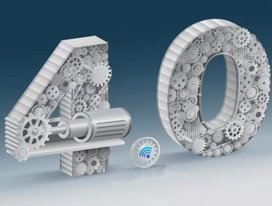
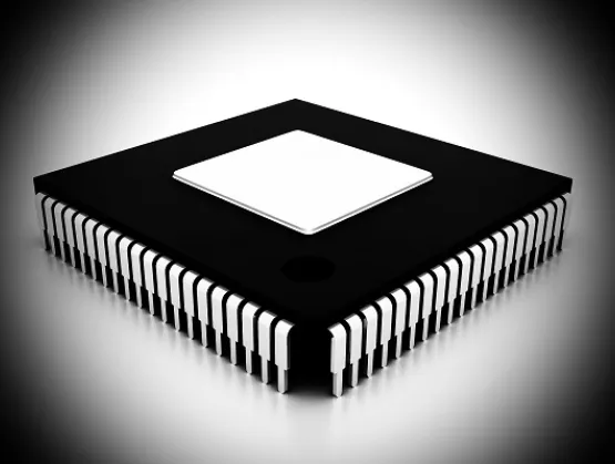
If you look at your clothes or shoes, there is a growing chance you will see the words Made in Vietnam printed on the tag. Since the United States lifted its trade embargo against Vietnam in 1994, the country has become the second largest exporter of apparel and shoes to the U.S. What may be less evident is the source of that new electronic gadget you received for Christmas, with its numerous parts, chips, and intricate supply chain. While light manufacturing has dominated Vietnam’s economic growth since the Đổi Mới economic reforms implemented in the 1980s, over the last decade the country has been repositioning itself to become a dominant player in the global microelectronics industry, a trend that has gained momentum in the wake of the U.S.-China trade war. In 2019, Vietnam ranked as the fourth largest exporter of electrical goods and components to the U.S. With exports doubling over the last four years and now exceeding $19 billion, surpassing Taiwan, Japan, and Korea (based on goods exported under chapter 85 of the Harmonized Tariff Schedule). Vietnam’s global electronics industry now accounts for about 40% of its exports, and the country seems to be just getting started. Early Entrants Though Vietnam owes its growing success in attracting foreign direct investment (FDI) in the semiconductor and microelectronics industries to the advent of China plus one – the business strategy to diversify business investments geographically – it was the few early entrants that gambled on this emerging market a decade ago that put Vietnam on the global stage. Of these early players, no other firm comes close to having the impact that Samsung has. It’s initial $670 million mobile phone manufacturing plant in the northern province of Bac Ninh in 2008 grew to a country-wide investment of $17.3 billion within a decade. Samsung is now Vietnam’s largest FDI contributor and accounts for more than 25 percent of its exports. Because of Samsung, Vietnam has become the second largest exporter of smartphones in the world. Around the same time, Intel opened its $1 billion semiconductor assembly and testing facility in Ho Chi Minh City, putting Vietnam firmly on the global technology map. More investors, like LG, Panasonic and Foxconn soon followed. Within a few years of these initial investments the industry was taking notice, illustrated by SEMI’s role in co-organizing the Vietnam Semiconductor Strategy Summits in 2013 and 2014. With SEMI SEA’s increased efforts to promote Vietnam as an important ecosystem in the electronics supply chain, more will be done to positively influence the growth and prosperity of its member companies in Vietnam. These early investors found Vietnam attractive for several reasons. Key among these are the country’s low wage rates combined with its favorable demographic structure – what the UN refers to as the golden population structure, which provides “Vietnam with a unique socio-economic development opportunity.” Companies are also attracted to the growing number of Free Trade Agreements (FTAs) that Vietnam belongs to, including the ASEAN Free Trade Area, CPTPP, the EU-Vietnam FTA, and, most recently, RCEP. Though the U.S. has yet to ink a trade agreement, the Singapore AmCham’s annual regional survey has consistently identified Vietnam as the most attractive country in ASEAN for a potential bilateral FTA partner with the U.S. Leveraging the Trade War If the plus one strategy was the catalyst that started this wave of electronics manufacturing in Vietnam, then the U.S.-China trade war was the enzyme that supercharged it. A common quip in Southeast Asia is that the U.S.-China trade war is over and Vietnam is the winner, and this is apparent in both trade and investment trends. According to the Asia Development Bank (ADB), the riff between the U.S. and China has caused a redirection in trade, as U.S. imports from the PRC fell by 12% in the first six months of 2019 while U.S. imports from Vietnam increased by 33%, with electronics and machinery accounting for the bulk of this jump. The ADB further reported that in a prolonged and intensified trade conflict, the worse-case scenario would result in Vietnam, Malaysia, and Thailand being the biggest winners, “in that order.” On the investment side, a March 2020 Gartner, Inc. survey of global supply chain leaders revealed that 33% had “moved sourcing and manufacturing activities out of China or plan to do so in the next two to three years.” While this survey did not mention specific winners, the ADB reported that “newly registered FDI in Vietnam from the PRC and Hong Kong rose by 200% year on year in the first seven months of 2019,” indicating the move of Chinese suppliers to Vietnam. Additionally, a review of recent press reports indicate firms like Apple, Nintendo and Dell are encouraging suppliers to move parts of their supply chains to Vietnam. These suppliers are complying, with Compal Electronics, GoerTek, HZO, Inventec, Luxshare Precision Industry, Pegatron, USI and Wistron all reportedly announcing plans for new investments in Vietnam. Manufacturing Hubs 
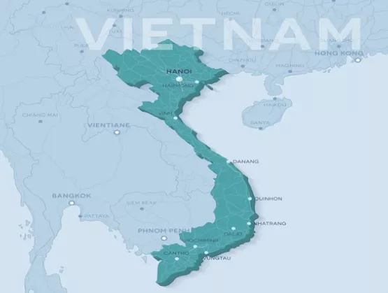
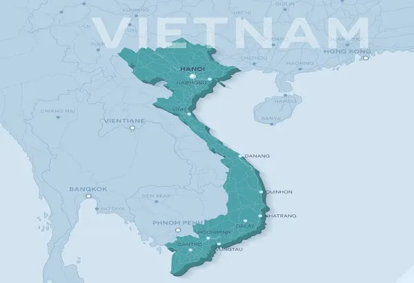
Within Vietnam, microelectronic facilities have concentrated in a few geographic hubs. In the south, the Saigon High Tech Park in Ho Chi Minh City attracted early entrants Intel and Samsung, with firms like Nidec and Jabil soon following. The largest investment capital, however, developed in the northern provinces that ring Hanoi. Bắc Ninh, an hour’s drive from Hanoi, was the site of Samsung’s first investment and has since attracted Foxconn and Canon. More recently, firms have been drawn to the port city of Hải Phòng, the country’s third largest city, which is already home to Samsung and LG. The city’s close proximity to other manufacturing clusters, its new deep-water port, and its expressway that provides a 12-hour trucking route to China’s electronics epicenter in Shenzhen are helping make the city Vietnam’s new high-tech production center. In 2019, LG Electronics moved its entire smartphone production line from South Korea to Hải Phòng, and in 2020 Pegatron reportedly chose the city for its $1 billion investment plan. Local phone manufacturer VinSmart is also producing the country’s first 5G smartphones in Hải Phòng. In November, USI, a subsidiary of Taiwan-based ASE Holding, broke ground on its first production base in Southeast Asia, a $200 million phase-one investment in the production and assembly of chips for wearable electronic devices. USI’s investment, which is moving into the internationally managed DEEP C Industrial Zones in Hải Phòng, is “intended to move us closer to our overseas customers and accommodate their ever-increasing demand,” according to Mr. Kuei Chun Chi, the firm’s Manufacturing Service Director. “North Vietnam, with its strategic geographical position and an extended infrastructure in place, offers USI an optimal way to facilitate fast and flexible response to customers' orders.” Though the Covid-19 pandemic has dampened the pace of new investments in Vietnam’s microelectronics industry, it has also amplified the country’s attractiveness to investors. Vietnam was successful in containing the outbreak through aggressive quarantine and contact tracing measures, and as a result its economy has the brightest outlook in the region. The ADB forecasts the country will be one of the fastest-growing economies in SEA in 2021, with GDP estimated at 6.8%. The Ministry of Industry and Trade is also reporting that several of the world's largest technology corporations plan to shift their production chains to Vietnam post-Covid-19, an indication that technology firms will accelerate relocation plans in 2021. Vietnam’s successful response to the pandemic, combined with its strategic location, low wage rates and foreign trade agreements, will ensure that the region continues to benefit from the shift in supply chains in Asia, making it the new destination for electronics manufacturing. About the Author Stuart Schaag is Principal at E-Ward Trade Consulting LLC, which assists firms that are expanding their presence in the global marketplace by creating strategies combining market analysis, business development, commercial diplomacy, and relationship building. He previously spent 25 years in various domestic and overseas positions in the U.S. Department of Commerce’s International Trade Administration. Stuart served as the Commercial Counselor at the U.S. Embassy in Hanoi from 2014-2018 and resided in Vietnam until 2020.
Read More
The SEMI Smart Manufacturing Americas Chapter, a key driver of the Global Smart Manufacturing Initiative, accelerates awareness of digital and data-driven strategies and implementations to help speed adoption of smart manufacturing. In 2021, the Chapter will focus on expanding its work across the industry to include academic and research initiatives. The semiconductor industry saw an unprecedented focus on improving digital monitoring of manufacturing activity in 2020, partially due to COVID-19. The Americas Chapter shared case studies on new tools and techniques for social distancing in fabs, aides for remote maintenance, and tips for remote workers. The Chapter also introduced its three pillars of Sensing, Connecting and Predicting and offered related programs. The Global Smart Manufacturing Conference (GSMC) highlighted the significance of universities and research institutions in the development of smart manufacturing with their focus on joint research for broad dissemination. To help drive smart manufacturing advances, at GSMC several offered non-proprietary tutorials on topic including the following: Integrating sensors for acquisition – CEA-Leti Applying new AI and ML tools and strategies to manufacturing – Binghamton University Digital tools for planning, qualifying and management and scheduling in fabs – MINES Saint-Étienne. Adding AI tools to robot work in a smart factory – KAIST Institutes By continuously highlighting the activities of these and other institutions through presentations, interviews, articles and blog posts, we will draw more attention to what is on the horizon for smart manufacturing in 2021. The SEMI Smart Manufacturing Americas Chapter also plans to elevate activities important to the Outsourced Semiconductor Assembly and Test (OSAT), Surface-Mount Technology (SMT) and Printed Circuit Board Assembly (PCBA) segments of the industry including programs on inspection, traceability and the SEMI SMT-ELS Standard for SMT automation. Thurston Taylor, marketing expert at Tokyo Electron and Vice Chair of the Americas Chapter, notes that “With increasingly more demanding requirements for bump, assembly and test, smart manufacturing and applied data science are necessary to achieve back-end goals now and in the future.” Also, many companies are implementing smart manufacturing applications and assessing various strategies to increase their smart manufacturing capabilities. Members of the Americas Chapter plan to review and develop self-assessment documents and maturity models that apply to front-end wafer fabs all the way through packaging and assembly facilities. “Moving forward it is imperative for all of us to up the intensity on specific ROI vectors such as quality, cost, productivity, sustainability and safety leveraging our smart manufacturing SEMI framework of Sensing, Connecting and Predicting,” said noted Bobby Mitra, worldwide director of Smart Manufacturing at Texas Instruments and Americas Chapter Chair. “By offering special flagship events, invited talks, ROI case-studies and ROI criteria in maturity models, we’ll bring high value to the smart manufacturing industry.” Chapter members also will begin mapping the skills needed to implement and support increasingly digital manufacturing capabilities, including any new skill sets, to help companies develop their hiring, training and management strategies. The mapping effort aims to support companies in building a strong pipeline of employees who can efficiently manage and operate smart manufacturing facilities. For its part, the Americas Chapter’s Go Green Subcommittee will focus on applying smart manufacturing technology to reducing the electronic industry’s carbon footprint by accurately tracking energy waste improving overall fab efficiency. Stay tuned for details on activities planned for our chapters in Europe, China, Japan, Korea, Southeast Asia and Taiwan. To learn more about each chapter and how to get involved, please visit the SEMI Smart Manufacturing Hub and sign up for our newsletter. Ayo Kajopaiye is senior project coordinator, Collaborative Technology Platforms, at SEMI.
Read More
Despite the pandemic lock-down, demand for electronic products and services remains strong. Work-from-home, video conferencing, and remote learning are driving data center growth and laptop and tablet demand. 5G infrastructure rollout is underway and smartphone sales are returning to normal levels. Automotive sales are increasing. At the same time, the industry is experiencing acute shortages of substrates. The October 2020 fire at Unimicron’s IC package substrate plant in Taiwan exposed the serious nature of the capacity shortage for IC package substrates. Substrate makers have been reluctant to make large investments in capacity over the last few years due to the fear that demand could decline and they would have excess capacity. Relentless price pressures by customers and the resulting low margins have weakened the finances of substrate suppliers. With tight capacity, substrate prices have increased and lead times are 14 weeks or more. The most critical shortage is for flip chip ball grid array (FC-BGA) substrates. In addition to increased demand in units, applications such as servers and networking products are seeing requirements for larger body sizes and increased layer counts. Shortages will not improve very soon because it takes time to build a new plant. And equip it. Key equipment for substrate production has lead times of up to a year. SEMI and TechSearch International detailed the substrate makers and provide projections for the substrate market, trends, and a list of suppliers and their plant locations in the Global Semiconductor Packaging Materials Outlook report. The report also highlights the market and suppliers for leadframes, bonding wire, encapsulation materials, underfill, die attach, solder balls, wafer level package dielectrics, and wafer-level plating chemicals. In times of shortages the report is an important indicator of suppliers in the industry and trends. Jan Vardaman is President at TechSearch International Inc.
Read More