downloadGroupGroupnoun_press release_995423_000000 copyGroupnoun_Feed_96767_000000Group 19noun_pictures_1817522_000000Member company iconResource item iconStore item iconGroup 19Group 19noun_Photo_2085192_000000 Copynoun_presentation_2096081_000000Group 19Group Copy 7noun_webinar_692730_000000Path
Skip to main content
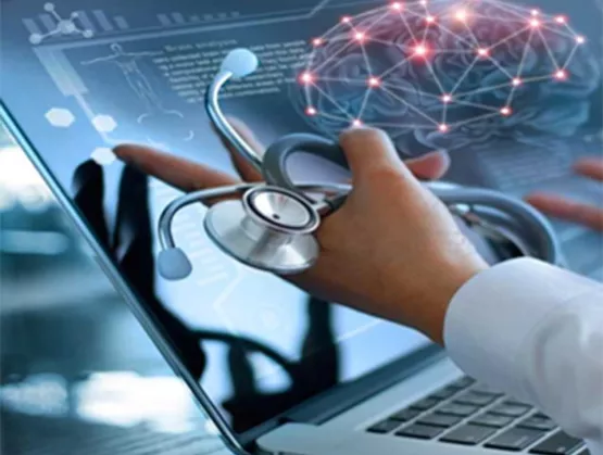
The recent global pandemic redefined well-established paradigms in healthcare. The classic model involving frequent hospital visits is no longer viable due to the risk of contagion. The focus is now on remote and pervasive vital sign monitoring solutions and automated data processing for health assessment. Social-distancing-friendly technologies, such as wearables, implantables, insertables and ingestables that enable long-term monitoring, can help detect medical abnormalities both in individuals and large populations. SEMI spoke with Carlos Agell, program manager and principal member of Technical Staff at imec, about remote vital sign monitoring using innovative form factors and methodologies. imec’s healthcare technology vison for remote care systems will be the focus of Agell’s presentation at the SEMI MedTech Forum, 19 February, as part of the SEMI Technology Unites Global Summit, 15-19 February 2021, online event. Join us to meet experts from imec and other key industry influencers. Registration is open. SEMI: What is driving innovation in diagnostics and what is the role played by the semiconductor industry? Agell: There is a clear need for remote diagnostics triggered by the COVID-19 pandemic. Two examples are respiration monitoring and SARS-CoV2 testing technologies. The fact that some of the more obvious symptoms of COVID-19 are respiratory has revealed a big gap in medtech: the need for low-friction, ambulatory, continuous and pervasive respiratory monitoring solutions. At imec we have been working on bioimpedance-based technologies (from chipsets to smartphone-enabled sensing devices) that can provide feasible solutions in that space. Hence, novel sensing modalities from the semiconductor industry can make a difference when it comes to remote ambulatory respiratory monitoring. On the other hand, SARS-CoV2 diagnostic technologies have become paramount during the health crisis. In this space there is a clear need to simplify, speed up and lower the cost of testing. Additionally, from a practical perspective society needs to prevent virus spreading. imec is spearheading an innovative semiconductor-based solution aimed at simplifying SARS-CoV2 testing by collecting aerosols from subjects’ breath using a silicon-based solution for analysis using the polymerase chain reaction (PCR) method, the gold standard in COVID-19 testing. Determining viral load in exhaled breath is a clear indicator of infectiousness, and detecting subjects with a high viral load is key when developing these rapid tests to facilitate economic recovery. A cost-effective and speedy though reliable SARS-CoV2 testing solution opens up possibilities for its use as gating mechanism (such as testing to allow access to facilities and prior to boarding a plane) to help jump-start some of the hardest-hit sectors in the economy, such as travel and hospitality (hotels and restaurants) by enabling more in-person interactions. SEMI: Please share more about imec’s commitment to improving the healthcare sector. Agell: imec R D is active in the field of remote unobtrusive respiration solutions, which are vital in treating respiratory system conditions such as asthma, chronic obstructive pulmonary disease (COPD) and COVID-19. These solutions rely on a combination of silicon chipsets, sensor integration and algorithms to interpret sensor data. As part of our effort to understand biological fundamentals, imec’s multi-electrode array (MEA) platform for heart-on-chip applications offers unparalleled capabilities to acquire high-density information (4444 electrodes/mm2) to enable extra- and intracellular recordings, electrical stimulation and impedance gauging to study patient-derived cardiomyocytes, cells that make up the heart muscle. imec is developing a rapid, low-cost SARS-COV2 test based on breath analysis (aerosol capture) aimed at a 5-minute analysis. Such tool is a key to economic recovery, and imec is planning large-scale testing of the prototype device at Brussels Airport later in 2021. imec has recently supported spinoffs and external companies that develop social distancing tools for usage during the pandemic. Healthcare is a key strategic area at imec, with multiple departments working on complementary topics, ranging from cell-sorting technologies and multi-electrode arrays, through sensors and systems for non-invasive cardiorespiratory and neurological monitoring, all the way to advanced processing of medical data and tooling for trials. SEMI: How is the pandemic impacting remote diagnostics? What’s new in that field? Agell: The pandemic has accelerated advances in remote diagnostics for healthcare – for example making remote doctor visits possible and launching telehealth into a successful sector. But in my opinion, this is just the starting point. Telehealth doctors will soon need to collect health data points such as body temperature, weight, or blood pressure remotely, the same information they collect during an office visit. Soon thereafter though, doctor’s will need more and more data, sparking the next stage of advances in remote diagnostics as algorithms are developed to analyze sizeable amounts of data. All in all, it will result in a big move from doctor-centric paradigms to more patient-centric solutions. Hopefully that jump will also drive a more proactive approach to health, enabling prevention and keeping people healthy, and leaving behind the era of curing the sick. imec research tools for respiratory monitoring will come in the form of a health patch. SEMI: Besides infectious disease diagnostics, what solutions will enable a paradigm shift? Can you name two global market trends related to the rising need for remote diagnostics? 
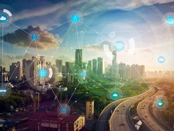
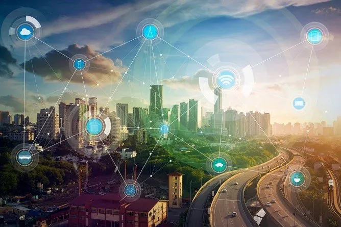
Agell: The paradigm shift in healthcare will be largely fueled by the hyperconnectivity trend. Communications are fast and far-reaching. The pandemic has proven that healthcare, similar to retail, banking, trading and business in general, can also be done partly remotely through a communications line. The need for proof of performance in the case of diagnostics has been proven challenging, due to the highly regulated medical field and the general conservativeness of this market. There is a clear trend underway in which algorithms and automated diagnostics are slowly gaining the trust of the medical community. Trials and regulatory submissions will help here, but the clear proof will be the general trust of the medical community (and general population) in solutions that have been on the market for a while. Similar to what happened with GPS navigation technologies back in the day, it would require a critical mass to reach general acceptance. As far as the healthcare market is concerned, there is a forecast bounce back from telehealth into hybrid models (a mix between in-office visits and telehealth) as a first post-pandemic scenario. Although this is perceived as the best of both worlds, its effectiveness and survival within the market is still to be proven. A clear market trend accelerated by the pandemic is the commoditization of health and wellness features in consumer electronics. A glimpse into consumer electronics venues reveals that watches, smartphones, weight scales and even your office chair or mattress will soon be collecting healthcare information. imec MultiElectrode Array (MEA) chipset SEMI: What is imec’s role in addressing the challenges and trends in healthcare? Agell: As an R D organization, imec offers expertise in the semiconductor, integration, data interpretation, data management and health-specific application domains. Thanks to our experience in horizontal technology and multiple application domain verticals (including healthcare), imec provides solutions to partners that push the boundaries of performance in health-tangential fields such as communications, consumer electronics, automotive and energy. imec is part of big European initiatives aiming to tackle the challenges of the pandemic. For example, we recently started working on the Digipredict project, which aims at early intervention in infectious diseases. We’re working with key players in the research domain within the EU such as École Polytechnique Fédérale de Lausanne, University of Twente and Eidgenössische Technische Hochschule Zürich. Additionally, imec has worked for market leaders in the healthcare sector such as Philips and Biotelemetry (recently integrated in Philips) and can help partners make the next health solution a reality. SEMI: How can technology unite us? What do you expect from your participation at SEMI Technology Unites Global Summit? Agell: I am a big optimistic on this pandemic. I believe technology has played a key role in putting boundaries around damage caused by the global health crisis. Technology does not only unite us, but it arguably saves lives! My personal expectation for the SEMI Technology Unites Global Summit is for us to get a better understanding about how the semiconductor industry reacts to a pandemic and upcoming post-pandemic scenario. I am curious to see if health-related trends emerge, and whether this is a transitory effect. During the last global pandemic, the semiconductor industry was not even existing, so there is no clear precedent for the current situation. Carlos Agell, program manager and principal member of Technical Staff at imec, where he oversees the development of projects and sets strategy directions for research topics. He has a background in wearable device development, having taken leadership roles in development of two FDA-approved medical devices in the field of wearable cardiology. He is member of the Dutch chapter of the standardization committee, which develops next-generation international standards for active medical devices. Carlos Agell holds two MSc degrees in Electronics Engineering and EECS from the Polytechnical University of Catalonia (Spain) and the University of California in Irvine (Irvine, CA, USA). Serena Brischetto is senior manager of Marketing and Communications at SEMI Europe.
Read More
As the Biden administration begins to advance its policy goals through U.S. government agencies, SEMI is eager to work with these new officials and appointees to advance innovation and strengthen U.S. leadership in the microelectronics industry. SEMI President and CEO Ajit Manocha today sent a letter to Commerce Secretary-Designate Gina Raimondo advocating for strengthening American manufacturing, investing in research and development and pursuing multilateral rather than unilateral U.S. export controls. SEMI also “requests Commerce perform a comprehensive review of recent policies and formally seek industry input via publication of a Notice of Inquiry (NOI), giving industry its first formal opportunity to provide its views on these significant regulations.” The letter discusses the importance of how export controls are implemented, advocating that “multilateral controls – where items of concern are controlled by all major producing nations – create a level playing field, maximize effectiveness, and minimize harm to U.S. national security and economic competitiveness. Unilateral U.S. controls over items for which there are comparable non-U.S.-origin items are generally ineffective in supporting national security goals and are likely to erode any technological advantages enjoyed by U.S.-origin items.” Foreign availability of semiconductor manufacturing equipment, materials and design software is an important consideration for U.S. export control policy related to those items. In an appendix to the letter, SEMI provided charts detailing the foreign availability of major types of semiconductor manufacturing equipment and materials. For nearly all items, there are competitive alternatives to U.S.-origin items available from non-U.S. sources. With many semiconductor technologies concentrated in a handful of key exporting nations, the letter encourages a unified approach via a plurilateral export control regime instead of unilateral U.S. controls for these technologies. SEMI provided a framework of issues that need to be considered and properly addressed in negotiating a plurilateral agreement related to semiconductor industry export controls. The previous administration created several unilateral controls that were implemented with little or no opportunity for public or industry comment and which created several unintended consequences. In addition to the request to publish an NOI, the letter asks Commerce to correct unintended controls related to the August 2020 expansion of EAR General Prohibition Three and reduce the backlog of license and classification requests. SEMI is pleased to work with the U.S. Department of Commerce and other policymakers by providing industry data, trends and perspectives to ensure export controls effectively serve national security interests without undue harm to technological development and leadership in this dynamic, globally competitive industry. Kimberly Ekmark is director of Public Policy and Advocacy at SEMI.
Read More
SEMI spoke with Eyal Shekel, senior vice president of Service Strategy and Excellence at Tokyo Electron Limited, about the impact of artificial intelligence (AI) on smart manufacturing and how other fab solutions for smarter process tools are advancing semiconductor manufacturing.Eyal shared his views ahead of his presentation at the SEMI Fab Management Forum, 17 February, as part of the SEMI Technology Unites Global Summit, 15-19 February 2021, an online event. Join us to meet experts from Tokyo Electron and other key industry influencers. Registration is open. SEMI: AI technology is considered a key enabler for smart manufacturing. What are the latest trends? Shekel: The advent of advanced nodes and extreme complex 3D semiconductor geometry has lengthened time to market and increased costs in areas ranging from equipment development and large-scale metrology usage to monitoring yield inhibitors.AI is becoming a critical tool in the area of material informatics to determine suitable materials and processing techniques in order to meet the needs of future devices. Together with new materials and processes, the development and implementation of virtual metrology will enable accurate and almost absolute real-time monitoring of our customers’ device wafers at each stage of the manufacturing process.SEMI: What are the benefits of data analysis in the process from R D and Ramp-Up to High-Volume Manufacturing? Shekel: The new research field of materials informatics enabled by AI provides tools to guide the highly efficient discovery and optimization of production processes. For example, TEL has developed methodologies for co-optimizing processes and materials for etch rates.To monitor and manage the yield of semiconductor fabrication processes, direct metrology measurements are important. However, it is difficult to monitor all production wafers due to the time and cost involved. With deep learning AI, it is now becoming possible to predict every wafer’s metrology measurements based on production equipment data and previously processed wafer metrology variables. This enables total quality management and run-to-run control, while simultaneously reducing production costs and cycle time.SEMI: Can you tell us more about TEL Service Advantage?Shekel: TEL Service Advantage is a TEL global support organization that allows customers to select a service plan that fits their needs. Through TEL Service Advantage, we can quickly respond to customer requests and technical advancements. TEL Service Advantage provides various plans to maximize equipment maintenance efficiency for customers and productivity from equipment manufactured by TEL. TEL Service Advantage plans can be combined to meet customer needs and achieve maximum results.A key enabling element of TEL Service Advantage is TELeMetrics™. TEL analyzes equipment data from various sensors using a remote connection and, based on that analysis, provides solutions to customer-specific problems around equipment throughput and predictive maintenance.SEMI: How is AI helping during the pandemic? Can you share a success story? Shekel: The pandemic forced severe travel restrictions worldwide, making it very difficult or even impossible in many cases to visit our customers, as it is still the case today. Standard communication devices like smartphones and email helped at the beginning when TEL intensified the remote support by our Total Support Centre (TSC).TEL continued to develop its Service Advantage program quickly, and started using additional advanced tools and methodologies such as the following: Deployed AR (Augmented Reality) to remotely assist our customer and TEL engineers Secured remote connections into TEL tools to investigate parameters and logs, or to change set-up Used remote training courses that connects trainers via video conferencing systems and training tools in the factories to skill up engineers located in a different parts of the world Used AR glasses for tool start-up and troubleshooting Expanded TEL database global technology with multi-tool on languages search capabilities A key project at a customer site in Europe offers an excellent success story. Using all the approaches above, we collaborated with the local team to put a tool into production with no major delays. This was highly appreciated by the customer and very important for us.SEMI: What do you predict for the future? Shekel: Global technology infrastructure continues to develop and expand rapidly. Elements like 5G networks, IoT and advanced sensing capabilities will lead to what we call General AI, which will be based on neuro-like infrastructure. The auto learning will spread across domains and rely on internal logic and reasoning to automate many tasks that are manual today. In our industry in particular, General AI will enable workers to focus more on data analytics and future advanced R D rather than ongoing operations.SEMI: How can technology unite us? What do you expect from your participation at SEMI Technology Unites Global Summit?Shekel: Technology united us in the last 150 years. The connectivity started with telegraph and telephone and was used to exchange information over wider distances. Nowadays, video conference capabilities, AR and improving communications technology makes it much easier to unite people who are geographically dispersed. This becomes obvious and valuable especially during this pandemic period. As a fact, we are able to continue to perform all our key activities – our tool support, training and customer relationships – even if we cannot be present in person.The SEMI Technology Unites Global Summit is a great chance to stay connected to people and customers that I would normally meet at the SEMICON exhibitions.It also offers the opportunity to network with many more people who I would not be able to meet otherwise. Moreover, I can watch speeches and presentations at any time! Normally I would miss some programs since exhibitions and events took place at the same time.Eyal Shekel, senior vice president of Service Strategy and Excellence at Tokyo Electron Europe Limited, is a 27-year semiconductor industry veteran. Upon his graduation as a Mechanical Engineer from the Technion (Israel leading technical institute), he joined Applied Materials. In 1997 he moved on to Tokyo Electron (TEL) in Europe, served as the Regional Service Manager of Israel and, soon after, was appointed the company’s General Manager. Since 2005 Eyal has been part of TEL Europe senior management. He oversaw the Service and Support Operations for TEL Europe as a senior vice president until 2019. In his current role, he co-leads TEL’s Global Service Committee in Japan.The SEMI SMART Manufacturing Initiative is a global effort to promote awareness of and interest in smart manufacturing with a focus on delivering industry-recognized best-in-class programs and services to enable members to maximize product quality and productivity while reducing costs. Activities are focused on building out core capabilities to enable smart manufacturing across the microelectronics supply chain. MADEin4 is a consortium of 47 partners from 10 countries connecting the full range of supply chain – from semiconductor equipment manufacturers and system-integrating metrology companies to RTOS and key applications such as the automotive industry. The MADEin4 Project develops next generation metrology tools, machine learning methods and applications in support of Industry 4.0 high-volume manufacturing in the semiconductor manufacturing industry. Serena Brischetto is senior manager of Marketing and Communications at SEMI Europe.
Read More
Back in 2012, China ranked fifth among seven regions worldwide in IC wafer capacity but surged past the Americas and Japan in 2018 and 2019 to claim the number three position (figure 1). That’s a big deal given that ICs account for the largest share of wafer capacity excluding discrete, opto, MEMS and sensors.China’s IC wafer capacity growth accelerated to tune of 14% in 2019 and 21% in 2020 and is expected to grow at least 17% this year, as we report in the latest update of the World Fab Forecast, published December 3rd by SEMI. Of all regions, Taiwan boasts the second strongest growth rate over the same period at 3% to 4%.Figure 1: Total IC installed wafer capacity for top five regions The report shows that from 2019 through the end of 2021 China will have increased wafer capacity for memory by 95%, foundry by 47% and analog by 29%. Foundry will represent the largest portion of those gains, reaching 2 million wpm (200mm equivalents). Memory will follow at about 1.5 million wpm and then analog at over 120,000 wpm.But Chinese companies aren’t pulling off this feat singlehandedly. Many international companies are contributing to the wafer capacity increases in China (figure 2). Figure 2: IC wafer capacity in China by company origin The share of capacity contributed by Chinese-owned companies and international companies has changed little since 2012, though Chinese-owned companies saw a slight dip in their slice of the pie from 60% to 57%From 2019 through 2021, Chinese-owned companies will add almost 60% capacity for foundries, the most of all sectors. Companies including SMIC, Hua Hong Semiconductor, Nexchip, XMC and Hua Li Microelectronics are driving the increases.During the same period, Chinese-owned companies will ramp up memory capacity from basically zero to 300,000 wpm. Companies such as Yangtze Memory Technology and ChangXin Memory Technologies (CXMT), also known as Innotron, are powering the quick rise with aggressive ramps of 3D NAND and DRAM capacity.Among international-owned companies, TSMC and UMC are driving the largest share of foundry growth, while Samsung, SK Hynix and Intel are powering gains in memory capacity.More information is available in the World Fab Forecast report. The report currently collects information for fab equipment and construction investment, capacities, technologies and product types for over 280 fabs and lines in China alone, including 40 facilities that either began operation in 2020 or will from 2021 through 2024.Christian G. Dieseldorff is senior principal analyst in the Industry Research and Analysis group at SEMI in Milpitas, California.
Read More
SEMI spoke with Dr. Franz Laermer, Research Fellow (Senior Chief Expert) at Robert Bosch GmbH Stuttgart, Corporate Sector Research and Advance Engineering, about the latest trends in medical diagnostics and personalized treatments. An open platform for the automation of complex molecular diagnostics workflows recently developed by Robert Bosch has proven its ability to take molecular diagnostics to the point of need.To make this happen, miniaturization, microsystems and microfluidics technologies, as well as microelectronics, are crucial. This is critical for the detection of SARS-CoV-2 infections within a rather short development time.Laermer shared his views ahead of his presentation at the SEMI MedTech Forum, 19 February, as part of the SEMI Technology Unites Global Summit, 15-19 February 2021, online event. Join us to meet experts from Robert Bosch and other key industry influencers. Registration is open. SEMI: What is driving innovation in diagnostics and what role does the semiconductor industry play?Laermer: One of the major drivers in diagnostics is the molecular breakdown and detailed analysis of nucleic acids on the level of the individual nucleotide. This reveals the root causes of diseases like cancer, genetic aberrations, infections and therapy resistances. Today’s solutions are mostly PCR-based (that rely on the polymerase chain reaction) or depend on sequencing. The keys to bring these technologies closer to the point of need are automation, miniaturization, low-cost, ease of use, flexibility, reliability, and fast time from sample-to-result. Semiconductor and microsystems technologies are enablers to meet these requirements, thanks to their ever-increasing performance, with Moore’s law pushing the semiconductor side of the story.SEMI: Can you tell us more about the the Bosch VIVALYTIC system? Laermer: VIVALYTIC is a universal and highly flexible diagnostic platform for the integration and automation of a wide variety of molecular diagnostics assays. It consists of the universal laboratory analyzer tool, which operates the application-specific cartridges. All reagents and specific bio contents are contained in the application-specific cartridges in a long-term stable manner at room temperature. The user only has to introduce the patient sample into the cartridge, push the cartridge into the analyzer and start the automatic workflow, which yields a diagnostic result within typically less than one hour. The VIVALYTIC products are manufactured by Bosch Healthcare Solutions GmbH (BHCS) in cooperation with strategic diagnostic partners and bio content owners.SEMI: How is the pandemic impacting automated diagnostics in the medical industry? What is new now?Laermer: The pandemic has clearly shown the importance of fast automated diagnostics at the point of need. Breaking infection chains as early as possible requires fast reliable PCR testing anywhere and anytime. We managed to reduce the time needed for SARS-CoV-2 rapid testing to less than 30 minutes for positive probes, an achievement that is embraced by our customers. Until a sufficiently high level of immunization is reached by vaccination, rapid testing is the only way to limit the number of infections, hospitalizations, and lethal outcomes of the COVID-19 pandemic.SEMI: Besides infectious disease diagnostics, what solutions will enable a paradigm shift in medical treatments?Laermer: Today more and more targeted drugs and therapies are developed in oncology to address certain mutations that are considered drivers of the cancer. This moves away from the one drug fits all approach to precision oncology. As a prerequisite of this personalized therapy, the mutation status of a tumor must be clarified – and monitored precisely and repetitively during therapy. The latter requires molecular diagnostics at the point of need, i.e. at the onco-ambulance. One keyword in this context is liquid biopsy. Another example of personalized therapy is the detection of bacteria type and antibiotics resistances in bacterial infections, and the selection of optimized antibiotics therapy.SEMI: What solutions can Robert Bosch bring to address the needs just mentioned? Laermer: Robert Bosch GmbH is a leader in microsystems, microsensors and semiconductor technologies. Our new 12-inch semiconductor plant in Dresden will strengthen our position in these fields. This encompasses artificial intelligence and the Internet of Things as well. As a technology provider, we generate superior solutions for automation and management of complex workflows, and thus deliver win-win-solutions together with our diagnostic partners.SEMI: How can technology unite us? Laermer: Technology, especially semiconductor and microsystems technology, is a game changer in the medical area. Whenever different disciplines meet each other and cooperate, as are the medical, diagnostics and semiconductor areas, innovation is accelerated strongly. New things happen at the interfaces between different areas of competencies.Franz Laermer, Research Fellow (Senior Chief Expert), Robert Bosch GmbH Stuttgart, Corporate Sector Research Advance Engineering. Dr. Franz Laermer joined the Corporate Research and Technology Center of Robert Bosch GmbH, Stuttgart, Germany, in 1990, where he started the development of new key technologies and sensor functions for the upcoming field of MEMS at Bosch. Today he is a Bosch Research Fellow/Senior Chief Expert for Microsystems, Microfluidics and Molecular Diagnostics. Laermer's work laid the foundation for the VIVALYTIC Diagnostics Platform of the newly founded Bosch Healthcare Solutions (BHCS) Business Division and the SARS-CoV-2 rapid tests from Bosch. Dr. Franz Laermer is the co-inventor of the Bosch Deep Reactive Ion Etching Process (BOSCH-DRIE) for microstructuring silicon. He holds more than 200 patents and was awarded with European Inventor of the Year 2007 – Category Industry prize by the European Commission and the European Patent Office (together with co-inventor Andrea Urban) for the invention, development and sustainable success of the BOSCH-DRIE process. He received the 2014 IEEE Jun-ichi Nishizawa Medal Award from the Institute of Electrical and Electronics Engineers (IEEE), USA. In 2019 he was awarded with the 2019 Technology Prize from the Eduard-Rhein-Foundation in Germany.Serena Brischetto is senior manager of Marketing and Communications at SEMI Europe.
Read More
Electric mobility, renewable energy and other technology innovations like IoT, 5G, smart manufacturing and robotics all require reliability, efficiency, and compact power systems, fueling the adoption of Silicon Carbide (SiC) and Gallium Nitride (GaN) to support lower voltages in significantly smaller devices. But chip designers must overcome the technological and economical challenges of integrating the two semiconductor materials into power systems.SEMI spoke with Elisabeth Brandl, Business Development Manager at EV Group about trends and new developments within the power electronics industry and the devices' application in smart mobility. Brandl shared her views ahead of her presentation at the SEMI SMART Mobility Forum, 18 February, as part of the SEMI Technology Unites Global Summit, 15-19 February 2021, online event. Join us to meet experts from EV Group and other key industry influencers. Registration is open. SEMI: What is driving new developments in power electronics?Brandl: Globally there are significant changes in infrastructure requirements for communication, automotive and power conversion. We need to look no further than the rising adoption of 5G, electric and hybrid vehicles, and renewable energy as examples of drivers of these changes. The device level, particularly in the field of power electronics, figures prominently in these shifts.The power electronics industry faces a growing number of scenarios where conventional silicon power devices are no longer suitable and are easily outperformed by new architectures mainly based on wide bandgap semiconductor materials like Silicon Carbide (SiC) and Gallium Nitride (GaN).SEMI: What industry challenges is power electronics innovation aiming to solve? Brandl: Power conversion efficiency is very important and needs further improvement as the related losses significantly contribute to the overall power consumption. For green power and a better environmental footprint, renewable energy is crucial, but so is overall power-consumption efficiency, yet the role of power devices is often underestimated. High-frequency and high-power applications, such as data center applications and inverters for renewable energy, where silicon power electronics are reaching their limits, are also important areas in power electronics.SEMI: How will the transition from silicon to compound semiconductor materials help?Brandl: The superior material properties of several compound semiconductors can tackle the need for lower losses in power conversion or better high-frequency behavior. Today, we mainly talk about GaN and SiC power devices as they are materials well-suited to address these needs. However, other materials like diamond and gallium oxide are in development for these applications. Material properties of SiC that enable thinner materials with lower power losses and better thermal behavior address power conversion efficiency as well as form factor challenges. GaN, especially in a high electron mobility transistor (HEMT), can be used for high-frequency applications.SEMI: What enables a better and more cost-effective manufacturability of SiC and GaN power devices?Brandl: For the end customer, a typical figure of merit regarding the cost effectiveness is $ per Ampere or Watt. While this seems simple, the reality is of course more complex. It is important to understand the main cost contributors within the manufacturing area. For SiC, this is clearly the substrate cost. In my presentation, I will show a way to reduce this cost via wafer bonding. For GaN, epitaxy – a method for growing or depositing mono crystalline films on a substrate – is the critical parameter. And of course, yield has a very big impact on cost effectiveness too, which means that good process control including metrology is very important.SEMI: Many semiconductor companies are already transitioning to silicon carbide and gallium nitride. Can you give us an example of a success story?Brandl: All the big power device manufacturers have either acquired or developed their SiC and/or GaN power device technology, so they also see a bright future for these wide bandgap semiconductors in the power device market. The most prominent success story is STMicroelectronics with its SiC MOSFET power devices, which have been implemented by Tesla in its Model 3 vehicles since 2018.SEMI: What is coming next?Brandl: New materials for power devices are being explored, such as diamond and gallium oxide. For SiC, the trend is moving toward 8-inch substrates, which is the focus of the funded EU project REACTION under the coordination of STMicroelectronics. Cost reduction and substrate availability also play a big role. All major power device manufacturers have contracts to secure the supply chain for SiC substrates because material availability is the main uncertainty at this time. Finally, collaborations along the supply chain are crucial and generally beneficial for all parties, as development requirements are better communicated and prioritized.Elisabeth Brandl is Business Development Manager at EV Group. She received her master in technical physics from the Johannes Kepler University Linz, Austria in Semiconductor and Solid State Physics. Since 2014, she has been responsible for Product Marketing Management for temporary bonding and compound semiconductors at EVG. The SMART Mobility Forum is the digital platform of SEMI Europe’s Global Automotive Advisory Council (GAAC) for industry stakeholders along the automotive and electronics value chains, from Design, Semiconductor Equipment and Materials Suppliers to Automotive OEMs.Smart Mobility is one of four SEMI initiatives focused on building communities, content, and activities around critical and emerging electronics markets. Read more about our Regional Chapters.Serena Brischetto is senior manager of Marketing and Communications at SEMI Europe.
Read More
The turn of the New Year means new opportunities for the microelectronic industry as SEMI continues to focus on a top priority for companies across the microelectronics design and manufacturing supply chain and SEMI members – supporting the development of the talent pipeline. Regardless of a member company’s role within microelectronics, ensuring a continued, robust flow of qualified talent for what is a cross-cutting, foundational industry sector is of high strategic importance. Skilled workers are essential to advances in areas such as artificial intelligence (AI), smart manufacturing, medtech, transportation and communications. In order to satisfy the world’s insatiable appetite for technology, we need a qualified workforce that can design and manufacture cutting-edge microelectronic devices. Launched in 2019 by SEMI’s Government Programs Office, SEMI Works™ is a holistic approach to developing and maintaining the talent pipeline. 2020 focused on building the all-important infrastructure, engaging member companies to identify required skills and developing a Unified Competency Model to catalog these workforce requirements. SEMI Works™ accomplished several firsts for the microelectronics industry: First dynamic, data informed workforce training standard adopted and published by the U.S. Department of Labor Employment Training Administration (USDOL-ETA) First SEMI Certified college program for technicians First Industry Approved Apprenticeship Program for Technicians, adopted and endorsed by the U.S. Department of Labor Member inputs anchor the SEMI Works™ portal, which enables connections among talent, employers and training/education providers. The portal’s initial phase of development is on track for completion in the first quarter of this year, marking the point when it will begin to be populated with specific job information, individual (talent) profiles and applicable training courses. Once SEMI Works™ is fully operational, it will be optimized to further support talent development and acquisition, providing a comprehensive platform for learning management, e-learning and career advancement. Throughout 2021 SEMI will be engaging members, training providers and job seekers to ensure the portal’s capabilities and user interface meets their needs. We’ll also move forward with several other SEMI Work’s programs including the Curated Content Initiative, which will enable SEMI members to identify non-proprietary courses, a SEMI member job board and an interactive career map to help job seekers plan their future in the industry. The microelectronics industry will only fulfill its tremendous promise for innovation and growth with the right talent. SEMI looks forward to working with members in 2021 to expand SEMI Works™ and help lay the groundwork for the next wave of technology advances. Mike Russo is vice president of Industry Advancement and Government Programs at SEMI.
Read More
Like TEL, many SEMI member companies have a long history of hiring veterans. We all have done a good job of hiring military personnel who possess the obvious semiconductor industry-related job skills and experience (e.g., avionics, hydraulics, mechanics, and radio frequency (RF)). But as an industry, are we doing enough? Are we missing out on the next employee of the year because we aren’t thinking broadly enough about our workforce? Five years ago, I met a young soldier at a military job fair. The interaction with him was a defining moment for me personally and it inspired me to commit to do more to translate military experience to the civilian workforce. Soldier: “What does TEL do?” Me: (Industry has a bright future, chips are in essentially everything including your military gear, etc.) Soldier: With disappointment, “Well, I don’t suppose I’m qualified to work at your company – since its technology.” Me: “Please stay for another moment, tell me your MOS (Military Occupation Specialty code) and job duties.” Soldier: “Ma’am, I’m a bomb specialist. I disable bombs.” Me: “Okay, let’s see if I get this right. You work with electrical schematics. It’s a given you follow instructions and guidelines, consider safety a p-r-e-t-t-y big deal, work under pressure, and you work with a team. Right?” Soldier: With excitement, “Yes, ma’am. And we have a squadron motto: “We have NO bad days!” Me: “Well then, you have the PERFECT background!” This conversation changed this soldier’s outlook on his career possibilities after exiting the military. He never imagined that the specialized training and experience he received as a bomb specialist would lead him to a role in the high-tech industry. He honestly believed he possessed no value to a civilian employer. It was moving to experience this gap of understanding face-to-face. Yet, this is a typical conversation between recruiters and hiring managers and military members. I could have easily let him walk away. Instead, I chose to invest 10 more minutes to learn more about what this soldier had to offer TEL. What is the key challenge around hiring military veterans? Disconnect. 90% of veterans surveyed faced challenges seeking civilian employment. According to Pew Research Center, only 1% of the entire U.S. population is qualified to join the U.S. military, and .5% (yes, that’s ½ of 1%) serve. This means 99.5% of the U.S. population has no direct working experience with the military. Civilian employers (recruiters, hiring managers, or employees) do not understand what the military does, the technical nature and responsibility of each role, or the extensive training each military member receives. And, veterans do not understand the civilian workspace. We truly have a gap translating military experiences and skills to the civilian workforce and vice versa. What are the benefits hiring military veterans? There are numerous benefits to hiring military veterans. Veterans are well-versed in cutting-edge technology. Today’s military is high-tech, state-of-the-art, and computer-based. Veterans are uniquely matched to our industry. Their jobs are highly technical and soldiers are extremely safety-conscious; they appreciate guidelines, follow directions, and possess a strong sense of team. Veterans are global citizens. Many military veterans have lived and worked in more than one country and speak more than one language. They tend to be culturally astute. Veterans have a winner’s psychology. Military members receive hundreds of hours of professional and technical training. They focus on a higher purpose and win as a team. Veterans practice accountability and leadership. Personal accountability is highly promoted. There is no room for excuses or acceptable reasons for mission failure. Everyone has the opportunity for a leadership role at some level and has modeling of what good leadership looks like. Hiring veterans aid diversity program issues over time. The military is a diverse group with 16% females and 44% people of color. Military personnel come from a wide variety of experiences – from across all 50 U.S. states with a variety of cultural and economic backgrounds. How can SEMI member companies truly effect change? Considering over 200,000 men and women exit the military annually, we have a significant opportunity to effect change by offering careers to those who serve while expanding our industry’s talent pool. Here are some initial ideas to get your company moving towards a more robust military outreach: Participate in the SEMI Foundation’s VetWorks Program: The Foundation is creating a toolkit to help member companies engage, hire, train, and retain veterans. This includes support for veteran-friendly messaging and recruiting, internships, training programs, and job fairs. This work will launch in Q2 of 2021 – contact Margaret Kindling at SEMI for details ([email protected]). Have a smart plan – Determine what positions make sense to focus on for veteran hiring. Start simple and grow your efforts over time. Set metrics for what percentage of your hires will be veterans. Recruiters can use simple key word searches to pull veteran resumes. Your company can attend military job fairs (in person or virtual) either at military installations or hiring events by organizations like Hiring Our Heroes, RecruitMilitary, etc. Offer diversity training related to hiring military veterans that focus on military vs. corporate cultures. Additionally, Society for Human Resources Management (SHRM) Foundation offers a Veterans at Work Certification Program available for all interested participants. Soldier For Life – This is an official U.S. Army program created to help connect current soldiers, retired soldiers, veterans, and their families with education, employment, and health and wellness resources and opportunities. If you are near a military installation, get to know the transition assistance program (TAP) officer or the base commander. You have to be persistent – the relationship will be worth it. Ask your network, including SEMI member companies, if they would share their military installation contacts. This is not a closed talent competition amongst our industry partners. Many companies who have a robust military outreach program are eager to share their stories to help you get started. It is simply the right thing to do to help each other make a difference for those who served. Internships/Mentorships/Fellowships. Ask your local military installation if they offer direct mentorships or internships. A great way to get started with internships is partnering with NAM’S Manufacturing Institute – Heroes MAKE America. Hiring Our Heroes is another great resource for fellowships. Let’s do more for those who served. Interested in starting an industry veteran network to share best practices? Please contact [email protected]. We can do this! Kathy Garner is Manager, Talent Acquisition, Global Mobility, and Contingent Worker Management at TEL. References Bradbard, D. (Institute for Veterans and Military Families, Syracuse University) Schmeling, J. (Student Veterans of America). The Recruitment, Hiring, Retention Engagement of Military Veterans. Retrieved from https://www.shrm.org/foundation/ourwork/initiatives/engaging-and-integrating-military-veterans/pages/veteransguidebook.aspx Parker, K., Cilluffo, A., Stepler, R. 6 Facts about the U.S. Military Changing Demographics. Pew Research Center. Retrieved from https://www.pewresearch.org/fact-tank/2017/04/13/6-facts-about-the-u-s-military-and-its-changing-demographics/ Reynolds, G. Shendruk, A. (2020, July 13). Demographics of the U.S. Military. Council of Foreign Relations. Retrieved from https://www.cfr.org/backgrounder/demographics-us-military Shifting Forward Consulting. Shift to the Civilian SUIT: How Veterans Can Successfully Navigate 3 Job Interview Challenges. (10/17/18). Retrieved from https://cherriedavis.com/veterans-successfully-navigate-3-job-interview-challenges/ SHRM Veteran Panel 2018. Retrieved from https://youtu.be/rgDUAALxTRg SHRM Veteran Panel 2018 Resources Bureau of Labor Statistics https://www.bls.gov/home.htm Heroes MAKE America http://www.themanufacturinginstitute.org/Initiatives/Military-and-Veterans/Heroes-MAKE-America/Heroes-MAKE-America.aspx Hiring Our Heroes https://www.uschamberfoundation.org/hiring-our-heroes Soldier For Life https://soldierforlife.army.mil US Department of Defense https://www.defense.gov/Our-Story/Our-Forces/ USO https://www.uso.org/
Read More