downloadGroupGroupnoun_press release_995423_000000 copyGroupnoun_Feed_96767_000000Group 19noun_pictures_1817522_000000Member company iconResource item iconStore item iconGroup 19Group 19noun_Photo_2085192_000000 Copynoun_presentation_2096081_000000Group 19Group Copy 7noun_webinar_692730_000000Path
Skip to main content
While Artificial Intelligence (AI) emerged in the 1950s, only in recent years have AI applications proliferated with the explosion of data and continuing improvements in Moore’s law that have driven rising processing speeds. Voice assistants, image analysis software, search engines, and speech and facial recognition systems were among the first applications to use AI. Today, adoption has spread to sectors such as agriculture, cybersecurity, healthcare, software development, e-government and the intelligent enterprise to generate jobs and help spur economic growth. The Edge AI Opportunity and the Microelectronics IndustryAI can be embedded in hardware devices such as advanced robots, autonomous cars, drones or Internet of Things (IoT) applications. Today, according to the EU’s digital strategy, data centres and other centralized computing facilities account for the vast majority – 80% – of AI data processing and analysis, with smart connected objects such as automobiles, home appliances and manufacturing robots that bring the compute function closer to the user representing 20%. The latter, known as Edge AI applications, are powered by edge-based machine learning chipsets, not the AI chipsets designed to run cloud-based machine learning algorithms.The EU’s white paper on AI published in February 2020 anticipates that the way data are stored and processed for AI applications will change significantly over the coming five years as edge computing applications proliferate. Most AI applications need to connect with devices that collect data and manage data flows. When the applications connect with cloud infrastructures to train large volumes of data for a machine learning model, the interface devices often require hardware support. Edge AI can minimize data transport by processing data directly from local devices to accelerate data analysis and decision-making and make data transport or accelerator hardware unnecessary, critical in reducing power consumption and enhancing data security for applications such as autonomous driving. Over the past 40 years, the ICT sector has been continuously increasing greenhouse gas (GHG) emissions despite efforts to shift to renewable energy. Cloud-based AI applications require an ICT infrastructure for high-performance computing and high-speed connectivity. According to MIT Technology Review, data centres’ AI workloads could account for a tenth of the world’s electricity usage by 2025. a mass update of cloud-based AI applications may significantly increase energy consumption, unlike with Edge AI. This is why the strategy for developing Edge AI is well-aligned with the EU’s Green Deal objectives. Europe aspires to play a leadership role in Edge AI to strengthen the sector’s competitiveness and protect the European digital sovereignty. Europe’s strong industrial competencies in embedded systems and microcontrollers will help the region promote development of European domestic AI solutions for emerging high-value IoT applications in industrial processes such as Industry 4.0, Connected and Automated driving (CSA), smart cities, climate action, healthcare, and national defence and security. With this strong strategic position in technology, Europe is well-positioned to invest to become the leader in the Edge AI global market.Preparing the Workforce for the Microelectronics IndustryTo design and manufacture leading Edge AI chipsets, European education providers and industry will need to work closely together to train the current and future workforces. Within the framework of the METIS project, a four-year project co-funded by the European Commission through the Erasmus+ programme, SEMI and imec deployed experts in the field to survey and interview focus groups. The survey identified the following key focus areas for workforce development: 1. True Capability of AI and Data Science With AI’s heavy dependence on data, the workforce of the future must be trained in areas of data science including data integrity to ensure quality, unbiased sourcing, collection and accurate analysis necessary to interpret huge volumes of data. Europe also needs to train the next generation of AI chip designers in data security and privacy – key challenges to the widespread deployment of Edge AI chips. 2. Climate Change, Sustainable Development Goals (SDGs) and Social Inclusion TrainingSince the industry must be able to develop Edge AI solutions to enable the digital transformation while limiting GHG emissions, microelectronics engineers need to be schooled in climate change and understand how their work contributes to meeting the United Nation’s Sustainable Development Goals (SDGs). Workplace diversity and social inclusion are also important target areas for education since Edge AI applications should serve various groups of people with different needs.3. EthicsChip industry workers must also be educated in ethical issues of AI related to the technology’s potential societal impact in the near future[1]. With AI applications capable of monitoring Internet searches based on users’ personal preferences and biases to deliver tailored advertising, news and other information, developers must recognize how the technology can influence thinking and behaviour of individuals and groups. This awareness can help developers strike a balance between supporting commercial interests and societal good so the microelectronics industry can ensure ethical implementation of AI. 4. Cross-disciplinary Skills Required for AIAI development requires a comprehensive, cross-disciplinary skill-set to be able to integrate the work of specialists from diverse educational, cultural and professional backgrounds critical to developing non-biased AI solutions. For example, in addition to technical expertise, microelectronics AI developers must be able to communicate clearly and work in close-knit teams with non-technical experts from business, law, medicine and the social sciences.What’s Next?The microelectronics industry has a tremendous opportunity to develop new chip-based solutions for AI architectures, and apply AI techniques to improve operational efficiencies of design and manufacturing. To seize this opportunity, the industry must work closely with education providers to groom the next generation of skilled workers. This tight collaboration is critical to designing and delivering specialised courses to college and university students as well as engineers now working in the chip sector. The stakes are high. By preparing workers to develop Edge AI chipsets, the microelectronics industry can help the world confront some of the greatest challenges it faces today.For more information, see SEMI Responds to European Commission White Paper on Artificial Intelligence.METIS is a Sector Skills Alliance project co-funded by the European Commission’s Erasmus+ Program and coordinated by SEMI. The four year project, launched in November 2019, will develop a Microelectronics Skills Strategy. Based on the strategy, the METIS project will design 43 training modules for 1,100 hours learning in four key areas of the microelectronics sector.We thank Patrick Blouet (STMicroelectronics) and Jeroen Geusens (imec) for their valuable contributions to this article.[1] Ethics of Artificial Intelligence and Robotics, Stanford Encyclopedia of PhilosophyDr. Yanying Li is senior manager of Collaborative Projects at SEMI Europe.Dr. Pushkar P. Apte is the strategic technology advisor for the Smart Data AI Initiative at SEMI
Read More
D-SIMLAB Technologies, a Singapore-based provider of simulation-based business analytics and optimisation software solutions, recently joined SEMI. I spoke with Peter Lendermann, the company’s co-founder and Chief Business Development Officer, about the company’s role in the smart manufacturing movement, how customers are benefiting from D-SIMLAB solutions, and what the future holds for smart manufacturing. Ng: What is D-SIMLAB’s mission?Lendermann: Our mission is to develop, market, and deliver high-performance simulation-based decision support solutions that enable corporations to enhance their performance in a sustainable manner leading to significant cost savings. In particular, we focus on semiconductor manufacturing material flow planning and optimisation but also do business in aviation where we help customers optimise their spare parts support operations. What these two domains have in common are three important attributes: They are capital intensive, their underlying operations are complex, and operations are also heavily affected by random, i.e. unpredictable events, which makes both planning and execution of manufacturing operations very challenging. D-SIMLAB is a spin-off from the Singapore Institute of Manufacturing Technology (SIMTech) under the Agency for Science Technology and Research (A*STAR). Our head office is in Silicon Island Singapore. We also have representations in Germany and the U.S. Most of our staff are industrial and computer engineers with up to 20 years of operations experience in their respective industry domain, as well as vast data analytics and software development capability.Ng: What solutions does D-SIMLAB offer to optimise semiconductor manufacturing?Lendermann: In the three-pillar smart manufacturing framework of Connect, Sense and Predict advocated by SEMI, our focus is on Predict though we emphasise the equal importance of the subsequent Act: Our solutions can Predict, for example, WIP waves or usage-based preventive maintenance due dates. But much more value-add can be realised once some decisions with regard to how to Act can be derived from such a prediction. The ability to pro-actively adjust action plans in a timely manner is essential to overcoming challenges arising from changing customer due dates, mix profile changes, untimely production line issues, and production capacity to be shared with R D lots effectively, so that ultimately our customers can enhance capacity, reduce cycle times and improve the due-date performance of their factories.To that end, our D-SIMCON solution suite spans the full spectrum of decision-support tools required to forecast, manage and optimise material flow – from operational scheduling and dispatching, WIP forecasting and dynamic and static capacity planning all the way to specific applications for fab load mix optimisation or for the enhancement of the product/layer dedication and resist allocation in the lithography area. Our solutions are implemented in numerous 6-, 8- and 12-inch wafer fabs operated by both IDMs and foundries worldwide with capacity ranging from 40,000 to 200,000 wafers per month.Ng: What are the key enablers of D-SIMLAB’s success?Lendermann: Our success lies in deploying production-ready solutions for our customers, allowing them to extract immediate value. Our solutions enable the portrayal of many domain-specific characteristics such as queue time constraints or specific equipment behaviour, which is absolutely essential to generating operationally feasible plans or schedules in order to be able to Act in the best possible manner according to what has been Predicted. Moreover, we have modules for automatic generation, calibration and maintenance of the underlying capacity model, including resolution of data inconsistencies as well as verification and validation of the model, to allow near real-time responses to continuously changing operations. And the associated optimisation approaches focus on creating maximum possible value with as few iterations as possible and within minimum time through smart heuristics and parallel computing infrastructure – a paradigm that is as powerful as it is cost-effective.Ng: What are a few of your more notable customer successes?Lendermann: As a result of the first implementation of our novel, multi-objective based Scheduler cum Dispatcher, a tool capacity gain of 8%, a transportation capacity gain of 10%, and an operator workload reduction of 25% were concurrently realised at one of the critical equipment groups in our customer’s fab. At another set of equipment groups in the same fab, a 7% increase of lots within the critical queue time limiting area was achieved.Another use case we successfully realised is fine-tuning of Preventive Maintenance plans: Based on a seven-day lot arrival forecast at each equipment generated with our WIP Forecaster, a recommendation is made when PM would be best possible without causing too much disruption in the WIP flow. The effect of this synchronisation of the PM plan with material flow enabled a dramatic reduction of the average queue lengths at critical equipment groups and the associated cycle times without incurring any capacity loss. Reduction of average queue length as a result of synchronising preventive maintenance with material flow. Ng: What challenges has D-SIMLAB been facing in the COVID-19 world?Lendermann: Obviously, software delivery projects have become more challenging for the time being since our engineers cannot be on-site frequently. But it also turned out that more and more services can be delivered remotely, which has the nice side effect of making the services more cost-effective for customers. Overall, we are confident that our solid customer base will enable us to sail steadily through these challenging times.Ng: Where does D-SIMLAB see the technological development heading?Lendermann: In the future, enriching decision support and manufacturing execution solutions with machine learning and other AI techniques will be critical in reducing dependency on human experience. This path is essential to making manufacturing operations fully Industry 4.0-compliant. D-SIMLAB will certainly be at the forefront of this development. Bee Bee Ng is president of SEMI Southeast Asia.
Read More
The global economy has started down a gradual path to recovery from COVID-19 in recent months as the world continues to combat the virus. Yet one sector – semiconductors – has shown impressive growth powered by a transformation hastened by the pandemic across industries ranging from education and work-from-home to healthcare.Semiconductor sales increased 12% in September to mark a second consecutive month of double-digit growth, and year-to-date semiconductor receipts as of September jumped 5.5% compared to the same period in 2019, according to SIA/WSTS.While this upward trajectory is encouraging, it pales compared to 2020 semiconductor equipment billings growth, with results from SEMI showing worldwide global chip equipment billings in September soaring to a new high of $7.6 billion this year. During the first nine months of 2020, aggregate equipment billings logged a 23.6% rise compared to the same stretch in 2019, surpassing $51 billion. Better still, the total semiconductor equipment market in 2020 is on track to beat the previous high of $64.5 billion set in 2018.Investments in China, Taiwan and Korea are fueling the chipmaking equipment spending surge. With big domestic and international fab projects in the works, China this year is projected to become the world’s largest capital equipment market for the first time, surpassing Taiwan, which will follow at a close second. Korea will rank third in equipment investments. Taiwan and Korea growth will come on the strength of equipment spending for manufacturing leading-edge semiconductors.Equipment billings in North America and Europe declined year-over-year as the automotive and industrial sectors suffered the heaviest blows from COVID-19. Investment momentum in both regions is expected to pick up in 2021 after automotive production recovers to pre-pandemic levels while factory automation will boost industrial demand.For more information about monthly equipment billing trends by region and equipment segment, please see the SEMI Equipment Market Data Subscription.Clark Tseng is director of Industry Research and Statistics at SEMI.
Read More
Over the next five years the Taiwan government plans to invest NT$1.546 billion to build the workforce direly needed for future semiconductor industry research and development. The largesse is a tribute to efforts by SEMI president and CEO Ajit Manocha to enhance the competitiveness of the semiconductor industry by stressing the importance of talent development during his annual visits with the Taiwan president. He has been instrumental in bringing together Taiwan government agencies and local industry representatives – two players in developing the talent pool of the future – to discuss workforce initiatives.As the talent gaps threatens to choke the long-term growth potential of the chip industry, Manocha has emerged as a passionate champion of workforce development. In a letter to more than 2,000 semiconductor companies worldwide, he urged to executives act together to build the workforce vital to industry growth. In 2018, he met with Taiwan President Tsai Ing-wen to discuss ideas for attracting and retaining skilled workers to help ensure Taiwan remains a top investment destination for high-tech multinationals.In early 2019, SEMI Taiwan established its SEMI Taiwan Workforce Development Council to promote talent and career development. Already, the group’s work is resonating in the global semiconductor industry. In September last year, Manocha joined executives from industry heavyweights ASE, MediaTek and TSMC in a visit to President Tsai to urge the government to pursue industry sustainability through talent development. President Tsai responded by instructing her staff to review government resources available for talent development, help drive public-private dialogue and partnerships, and form talent development projects involving the government, industry, academia and research institutes.To carry out comprehensive workforce initiatives, SEMI Taiwan continues to work with the National Security Council and the Executive Yuan (the cabinet). We also launched the Semiconductor Industry Development Council in partnership with leading high-tech companies in Taiwan including ASE, TSMC, MediaTek, PSMC, VIS, MXIC, Nanya, Etron and UMC. Focused on developing semiconductor talent and technology, localizing equipment sourcing, and improving cybersecurity, the council has formed the following seven initiatives: Make existing government talent development programs more flexible to better meet the industry’s workforce needs. Recruit outstanding scholars and leading experts in scientific research, and solicit world-class scientific research teams. Extend age restrictions and other requirements for the Einstein Program (established by the Taiwan MOST, Ministry of Science and Technology) to attract outstanding foreign scholars to Taiwan. Establish a domestic semiconductor research ecosystem and provide sufficient research funding to cultivate R D talent. Strengthen female education in STEM (science, technology, engineering, mathematics) and encourage women to re-join the workforce to help meet the industry’s workforce needs. Continue to promote MOST University-Industry Collaboration Projects (Large Alliance) to connect the upstream academic and research sector with downstream industries. Encourage cooperation between science and technology universities and the chip industry to develop the talent necessary for smart manufacturing to thrive. SEMI’s advocacy efforts with the Taiwan government, the industry and academia are clearly paying off. The Executive Yuan recently announced three major talent development strategies – expanding the talent development capabilities of higher education institutions, promoting industrial-academic cooperation and encouraging businesses to strengthen recruiting efforts and increase funding for semiconductor talent development.The building momentum includes plans by the Taiwan Ministry of Education plans to establish semiconductor technology research centers at several national universities. By passing the sandbox law and loosening regulations organizational personnel, finance and education, the government is freeing up more funding to support semiconductor industry talent development. The ministry also plans to gradually expand the number of students enrolled in STEM curriculum and continues to promote talent training programs and recruiting strategies to help close the workforce gaps and reduce related industry risks. A highly skilled workforce is indispensable to the development of the semiconductor industry and among the most strategic resources in any region. It’s only through long-term partnerships between the government, industry and academia that impactful and sustainable workforce development goals and initiatives can be developed to help the chip industry realize its full potential to innovate and solve some of the world’s greatest challenges. The programs are key to the ability of Taiwan’s semiconductor industry to sharpen its competitive edge. More importantly, they are also the center of gravity in the region’s pursuit of its position as the global semiconductor hub. Jo-Ann Su is senior director and Winnie Chang is marketing and public relations specialist at SEMI Taiwan.
Read More
The air we breathe is precious yet neglected as anthropogenic pollutants continue to pour into the earth’s atmosphere. Still, there’s hope that greenhouse gas emissions – and the human behavior behind them – can be brought under control for the good of the planet with the help of gas sensors that gauge pollutant levels.Of the many air pollutants, some are more detrimental to our health than others. Figure 1 lists the top seven pollutants, their chief sources and health effects. The Air Quality Index is calculated by combining values from particles and four gases (carbon monoxide, ozone, sulfur dioxide, nitrogen dioxide). The good news is that gas sensors are available in the market that can monitor each of those pollutants.Figure 1 – Top seven pollutants and their health effects. Source: EPA Air Sensor Guidebook The challenge is that many gas sensor end users today have little understanding of how to compare the performance characteristics of sensors offered by various vendors. SEMI is working to help end users clear that hurdle. SEMI-MSIG this year created a group within its Device Working Group focused on developing gas sensor standards aimed at growing the market and defining guidelines affecting areas including testing methods, reliability requirements, packaging and communication interfaces. Importantly, the standards will also make it easier for end users to make a clear choice among rival products.The SEMI-MSIG Device Working Group comprises devoted experts from leading gas sensor companies as well as OEMs. We welcome companies involved in deploying gas sensors to join this fast-growing group to improve air quality standards in sectors including residential construction, factory automation, automotive, consumer electronics and healthcare. One potential market is consumer electronics such as smart phones since concerns about air quality is growing among device users.The MEMS Sensors Industry Group (MSIG) Device Working group was formed in early 2019. Its mission is to develop a series of technical specifications, industry standards and best practices for MEMS and Sensor devices and platforms. The goal is to advance the use and expansion of MEMS and sensors worldwide.Table 1 – Top seven pollutants and their health effects. Source: EPA Air Sensor Guidebook In the past, we focused on inertial sensors (See IEEE2700 standard for inertial sensors as an example of an output of this team). In 2020, our focus shifted to gas sensors and we plan to expand our work to include other types of sensors in the near feature. Industry leaders such as Bosch, TDK Invensense, Renesas, Infineon, Analog devices, STMicroelectronics, GE and Intel meet every month to strategize on a series of initiatives.If you’re interested in joining the SEMI-MSIG Device Working Group, please contact Carmelo Sansone, Director of MEMS Sensors Industry Group.The MEMS Sensors Industry Group (MSIG) is a SEMI technology community that enables the MEMS and sensor industry to address common challenges, innovate and accelerate business results.Carmelo Sansone is director of the SEMI-MSIG. He has focused his career on building products and system solutions that have large impact in the marketplace. Sansone launched several sensor processor platforms for low-power applications, including the first microcontrollers with DSP capabilities, the core of today’s portable devices intelligence. Sansone has led the successful integration of the MSIG organization into SEMI by expanding its services and global reach. Carmelo holds a master’s degree in Electronic Engineering with a specialization in Biomedical from the University of Pisa and an MBA from Golden Gate University, San Francisco.
Read More
As the United States government has expanded semiconductor-related export controls, companies in the global electronics manufacturing and design supply chain have had to spend considerable time and effort navigating restrictions and managing significant new uncertainties emanating from recent policies. On November 9, SEMI submitted comments to the Department of Commerce’s Bureau of Industry and Security (BIS) urging the agency to proceed cautiously and adopt regulatory best practices and microelectronics industry recommendations to ensure that its identification of foundational technologies does not restrain U.S. innovation and exports without furthering essential U.S. national security interests. The comments specifically respond to the August 27 Advance Notice of Proposed Rulemaking (ANPRM), Identification and Review of Controls for Certain Foundational Technologies. The Export Control Reform Act (ECRA) of 2018 required BIS identify certain emerging and foundational technology that is “essential” to U.S. national security and requires such technology to be controlled to China and other nations subject to a U.S. arms embargo. Congress did not provide a specific definition for emerging or foundational technology, nor the term essential, further complicating the process to identify such technology.BIS has already implemented or proposed several emerging technology controls and the ANPRM starts the process to identify potential foundational technology controls. The SEMI comments focus on the fundamental question of how to define foundational technology, and are organized into three main sections: Requirements of ECRA Guidance from ECRA Regulatory best practices and industry recommendations Applying the statutory requirements and guidance, together with best practices and recommendations, to the identification of foundational technology indicates that most semiconductor-related technology, particularly semiconductor manufacturing equipment and materials, should be outside the bounds of the foundational technology initiative. In general, most technology related to semiconductor devices, manufacturing equipment, materials and design software is not essential to U.S. national security and, in cases where such technology does present material national security issues, it is generally subject to the U.S. list review process and multilateral controls. This technology is widely available outside the United States and due to substantial foreign availability, unilateral U.S. controls on such technology are likely to be ineffective in limiting its proliferation and harm U.S. development of or threaten U.S. leadership in this technology.While the SEMI comments focus on the effort to identify foundational technology, the recommendations and best practices apply in all export control contexts. Several of the statements pertain to policy in ECRA, including its imposition of controls to further specific essential U.S. national security interests only after full consideration of their impact on the economy.Other statements derive from factors ECRA requires BIS to consider, such as not seeking to control technology that’s already available outside the U.S. and not imposing controls that would harm U.S. technological development or leadership. An additional key factor is not imposing controls before multilateral controls are agreed to, nor when it is unlikely the relevant multilateral regimes will adopt similar controls, as is likely for technology that has been decontrolled by a regime.Finally, regulatory best practices suggest that technology-based controls should not be imposed when more targeted end-use or end-user controls can address national security concerns and duplicative controls in addition to recent, significant expansions of existing controls are unnecessary.SEMI is pleased to work with the U.S. Department of Commerce and other regulatory agencies, providing industry data, trends and perspectives to ensure export controls effectively serve national security interests without undue harm to technological development and leadership in this dynamic, globally competitive industry.Ways to Stay Connected and Learn MoreSEMI is committed to serving the global electronics manufacturing and design supply chain and present the collective voice of members to governments worldwide.The SEMI Global Update weekly newsletter provides updates on advocacy issues and technology trends and is available to all.Additionally, SEMI hosts live and virtual events that offer analysis and insights of geopolitical trends by industry experts, with the next opportunity to participate coming on December 3 with the SEMI CEO Webinar: Analyzing the Impact of the U.S. Election on the Microelectronics Industry.Joe Pasetti is Vice President of Global Public Policy and Advocacy at SEMI.
Read More
Global business conditions continued to improve through October although the rate of improvement slowed a bit as pandemic concerns increased (Chart 1).Electronic Equipment Shipments RecoveringThird-quarter world electronic equipment shipment growth showed a big improvement over the second quarter but was still down an estimated 1.4% compared to the same quarter in 2019 (Chart 2).Based on regional electronic equipment shipment data, October 2020 sales were up 3.5% versus October 2019 and up 6.1% sequentially versus September 2020 (Chart 3). As the traditional autumn busy season winds down, the key impediment to a strong recovery is the rising COVID-19 infection rates, especially in the United States and Europe. The world awaits the deployment of a much-needed vaccine.Semiconductor Growth May be EbbingSemiconductor chip shipments continue to increase but their global rate of growth has leveled off to mid-single digits (Chart 4). Wafer foundry sales growth also appears to be peaking (Chart 5), pointing to slower chip growth in coming months.SEMI Equipment ShinesSemiconductor capital equipment shipments continue to outshine both electronic equipment and semiconductors. Third-quarter 2020 SEMI global sales were up a whopping 31% compared to the same quarter in 2019 and up 16% versus the second quarter of 2020 (Chart 6). SEMI equipment shipments are definitely outpacing semiconductors on a 3/12 growth basis (Chart 7).SEMI Outpaces Electronic Supply ChainGlobal electronic supply chain growth is improving but the semiconductor sector is clearly the winner this autumn (Chart 8).Looking Forward, Pandemic Spread is Biggest WorryBusiness conditions definitely look brighter. Even stronger growth is likely if we can get COVID-19 under control.Walt Custer of Custer Consulting Group is an analyst focused on the global electronics [email protected].
Read More
COVID-19 has had an impact on the entire healthcare market. During the peak of the first wave, companies from the industrial and automotive sectors worked on repurposing their sensors and production lines to provide pressure sensors for respirators and temperature sensors for thermometers. At the same time, companies making sensors for wearables and other mobile devices used for remote monitoring of patients experienced saw increased demand, caused in part by the surge in telemedicine worldwide. In addition, strong demand for COVID-19 tests pushed diagnostic players to repurpose existing systems to detect the SARS-CoV-2 virus or associated antibodies. Over the past six months in particular, numerous microfluidic technologies have enabled either rapid point-of-care tests or high-throughput solutions for central labs. The demand for these tests is incredibly high (millions of tests per month are needed), which has contributed to boosting the revenue of many companies in the respiratory-testing area.These respiratory-testing companies have placed many testing machines at existing and new customer sites, and have sold an impressive number of test kits resulting in an initial revenue spike in Q1 2020, and even higher spikes in Q2 and Q3. This growth seems on track to last into early 2021 and beyond as the pandemic continues, the flu season arrives, and health organizations test increasingly higher numbers of people than they were several months ago. The winners in respiratory testing include Abbott, bioMérieux, Cepheid, GenMark and Luminex, among many others. In this context, Yole expects the point-of-care segment of the microfluidic product market to enjoy an impressive jump from US$4.5 billion in 2019 to US$6.3 billion in 2020, growing at 15.1% CAGR between 2019 and 2025 to reach $10.4 billion in 2025. This represents 40% of the total microfluidic product market in 2019.In its research on microfluidics, Yole tracks a wide range of COVID-19 tests from different companies. The tests are used to meet different needs. Evolution of COVID-19 TestingNo doubt this increased production of tests will be especially useful for the upcoming flu season. But what will happen next year, if (we hope) reliable COVID-19 vaccines are validated and marketed, and the new coronavirus eventually disappears? Will diagnostic companies’ sales fall to pre-pandemic levels, and all these investments in production lines be wasted? Don’t worry. This is not a one-shot deal: Once the pandemic is over, most testing machines will remain in place, and customers will use them to run other tests the companies offer – usually for other kind of infectious diseases – driving sales of single-use disposables in coming years. The pandemic has shown us that more efficient diagnostic tools are required. Rapid, inexpensive, widely accessible testing for infectious diseases is crucial if we are to face such challenging situations. The real struggle for diagnostic companies, especially in the field of microfluidics where recent platforms have a small assay menu, is placing instruments (i.e., the test machines that run the disposable cartridges and read the results) at customers’ locations, from hospital settings and urgent care to field testing sites, and this has now been achieved. This will drive consumables sales in the future, even beyond the pandemic, and take the microfluidic-based point-of-care testing market to the next level. Rapid point-of-care testing is driving growth in microfluidics and will continue to do so for years to come. In the meantime, new significant opportunities are opening for point-of-care diagnostic test-makers, and rapid, miniaturized microfluidic technologies may be the winners here. Rapid passenger screening in airports, and rapid employee or visitor screening at the workplace will become essential for preventing the virus’ spread. In total, this could represent billions of rapid tests needed per year. COVID-19 has slowed down business growth in many areas but has really helped microfluidic-based point-of-care diagnostics take it to the next level, and this is only the beginning.For more information on Yole’s microfluidics activities, please view Yole’s reports, Point of Need 2020 – Including PCR-Based Testing or Status of Microfluidics Industry 2020 or visit i-Micronews.comYole Développement is a member of SEMI and the MEMS Sensors Industry Group (MSIG), a SEMI technology community that connects the MEMS and sensors supply network in established and emerging markets enabling members to grow and prosper. Visit us today. Sébastien Clerc is a technology and market analyst in Microfluidics, Sensing Actuating at Yole Développement (Yole). As part of the Photonics Sensing team, Clerc has authored a collection of market and technology reports dedicated to microfluidics and other micro-devices for major market segments: medical (including diagnostics, pharmaceutical, biotechnology, drug delivery, medical devices) and industrial (including environment, agro-food). At the same time, he is involved in custom projects such as strategic marketing, technology scouting, and technology evaluation to help academic and industrial players in their innovation processes. Thanks to his technology and market expertise, Clerc has spoken in more than 20 industry conferences worldwide over the last four years. Clerc holds a master’s degree in Biomedical Technologies and a master’s degree in Innovation and Technology Management, both from Grenoble Institute of Technology (Grenoble INP - Grenoble, France).
Read More
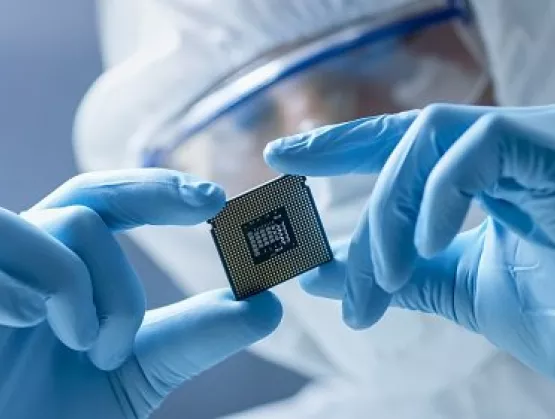
PNI Sensor, a member of the SEMI-MSIG Positioning, Navigation and Timing (PNT) Technical Advisory Council, is developing advanced tracking systems that promise to increase industrial worker safety.The availability of low-cost GPS jamming and spoofing technologies renders GPS-only solutions for location and navigation an increasingly dangerous and ineffective choice for the dismounted soldier in a battlefield environment. This threat to armed forces has spurred development of new self-contained location and navigation technologies for defense applications — an innovation that offers significant advantages for commercial applications.Though not as complex and mission-critical as in defense, self-contained location technology is also essential in commercially available industrial applications. That’s particularly true for workers in industrial sectors such as utilities, mining, and construction, and in environments with lone or remote workers, such as first responders. While jamming and spoofing are not a threat in the industrial sector, determining the precise location of workers in GPS-denied environments is fundamental to ensuring their safety. This makes it a priority to adapt any self-contained, non-infrastructure-based location technology — which was first developed for the modern dismounted soldier — to industrial applications.Bodies in MotionInertial solutions are very difficult to implement properly, even without the challenges uniquely created by human motion dynamics. On a construction site, for example, workers tend to cover a wide range of disciplines: supervisors, electricians, iron workers and equipment operators, among others. While performing their jobs, construction workers change locations, both indoors and outdoors, and perform dynamic motion such as crawling, ducking and climbing. These are all motions that are very difficult to model using traditional adaptive filtering techniques, which are typically applied in vehicular inertial navigation platforms, such as aircraft, ships and tanks. Even if existing inertial navigation systems could be made size, weight, power and cost (SWaP-C)-compatible to be body-worn, their performance accuracy would still need to satisfy the application’s requirements. To properly determine a worker’s precise location to ensure safety on job sites and in remote locations, we must tackle the combined challenges of SWaP-c and human dynamic motion. That’s the most effective approach for creating a complementary positioning technology that augments GPS or other infrastructure-based location systems.To address these challenges, we need to build a high-performance inertial measurement solution using commercially available MEMS inertial sensors. The issues of bias drift error and low sensitivity have traditionally made such sensors practically useless for any meaningful inertial tracking. Fortunately, this is no longer the case. We now have sensors that already conform to the necessary SWaP-C requirements for the application, and have the additional advantage of high dynamic range of measurements without saturation errors, which helps to reduce high-force and rapid movement-induced errors, promoting greater accuracy.Thus, a path forward is emerging. The current generation of high-performance MEMS gyros can now inertially track workers’ locations to step-level resolution very well for up to 30 minutes — without significant location errors due to bias or scale errors. That’s an order of magnitude better than previous generations. With the new MEMS gyros, errors typically remain less than 2% of distance travelled over that time period. Strategically applying algorithm improvements with higher levels of magnetic corrections has the potential to bring that accuracy down even lower, to less than 0.5% of distance traveled for durations of one hour or more. What’s more, the improved gyro and accelerometer bias, gain, and signal-to-noise (SNR) performance allows for better magnetic anomaly rejection. This enables finer and more sustained gyro bias corrections in the fused solution, which creates a system greater than the sum of its parts. We believe that these newer systems will promote greater worker safety at a truly affordable price.PNI Sensor, a member of the SEMI-MSIG PNT Technical Advisory Council (TAC), is developing a tracking system that combines the best elements of the newest-generation MEMS devices with an electronic compass that uses advanced magnetic anomaly detection and rejection algorithms. Based on PNI’s latest attitude and heading reference system (AHRS), the novel PNT system employs a unique Kalman algorithm that intelligently fuses its reference magnetic sensors with gyros and accelerometers. In conjunction with this work, PNI Sensor has developed advanced pedometry functionality for use in its tracking system for very high dead-reckoning tracking performance used in defense industry applications. PNI is initially designing that system to track dismounted soldiers and special forces operating in GPS-denied or contested environments.For more information about PNI Sensor’s advanced location and navigation technology, please visit PNI Sensor. To learn more about the SEMI-MSIG PNT TAC, please contact Carmelo Sansone, director, MEMS Sensors Industry Group.George Hsu is a founder and CTO of PNI Sensor. He has focused his career on the sensor industry, having invented several magnetic sensor breakthroughs, including the magneto-inductive technology, the core of today’s electronic compassing in the automotive, consumer, scientific and military markets. Hsu is a graduate of Stanford University School of Engineering, holds several patents, and is a much-published author of technical articles on sensor theory, design and applications. He is an active member of the MEMS Sensors Industry Group PNT TAC.About the SEMI-MSIG Positioning, Navigation and Timing ProjectMEMS Sensors Industry Group (MSIG) created a member-based PNT TAC to identify and pursue PNT system innovations for GPS-denied environments. To that end, MSIG solicited proposals from its membership for the SEMI-MSIG PNT Project, a U.S. Army Research Laboratory-funded R D project. PNT committee members that have secured funding are pursuing R D platforms that improve accuracy and performance. Platforms may include software, hardware, and advanced packaging requirements of optical and MEMS-based positioning and timing systems.
Read More