등록안내

사전등록은 9월 19일(금) 오후 5시에 마감됩니다.
[사전등록]
- SEMI회원사/학생: 198,000
- 비회원사: 231,000
[현장등록]
- SEMI 회원사/비회원사: 253,000
※ 상기 가격은 부가세 포함 가격입니다.
OVERVIEW
- 교육명: SEMI 반도체테스트기술교육 2025
- 일정: 2025년 9월 26일(금) 오전 9시 – 오후 5시 50분
- 장소: 수원컨벤션센터 401호
- 주최: SEMI Korea
NOTICE
- 교육내용 및 순서는 강사 사정에 의하여 임의로 변경될 수 있습니다.
- 본 교육은 고용노동부 환급과정이 아닙니다.
- 등록비에는 교재비가 포함되어 있으며 교육 당일 교재를 현장에서 수령하실 수 있습니다.
- 중식이 제공되며, 주차비는 지원하지 않습니다.
- 참석확인증은 교육 종료 이후 SEMI Korea 통합등록사이트(http://semi_prog.sjinfotec.com)에서 사후설문조사를 완료하시면 직접 다운로드 받으실 수 있습니다.
CONTACT
- 문의: SEMI 프로그램팀 (02-531-7831 / [email protected])
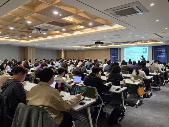
TESTIMONIALS
- Wafer Tester 개발자로서 테스트 방식에 대해 다시 한번 배울 수 있는 기회였고, 다른 강의보다 많은 도움이 됐습니다.
- 테스트 기술 동향파악에 도움이 되었습니다.
- 실제 업무 관련 내용을 이해하기 쉽게 설명해 주셨습니다.
(2024년도 참석자 후기 발췌)
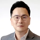
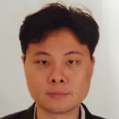
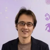
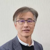
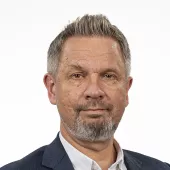
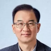
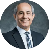
SPEAKERS FROM
 |  |  |  |  |
대한민국
수원컨벤션센터 401호
Welcome

Semiconductor Test and Market
- Semiconductor Market
- IC Manufacturing process
- ATE system architecture
- ATE Instrument structure
- Introduction of IC test
Break
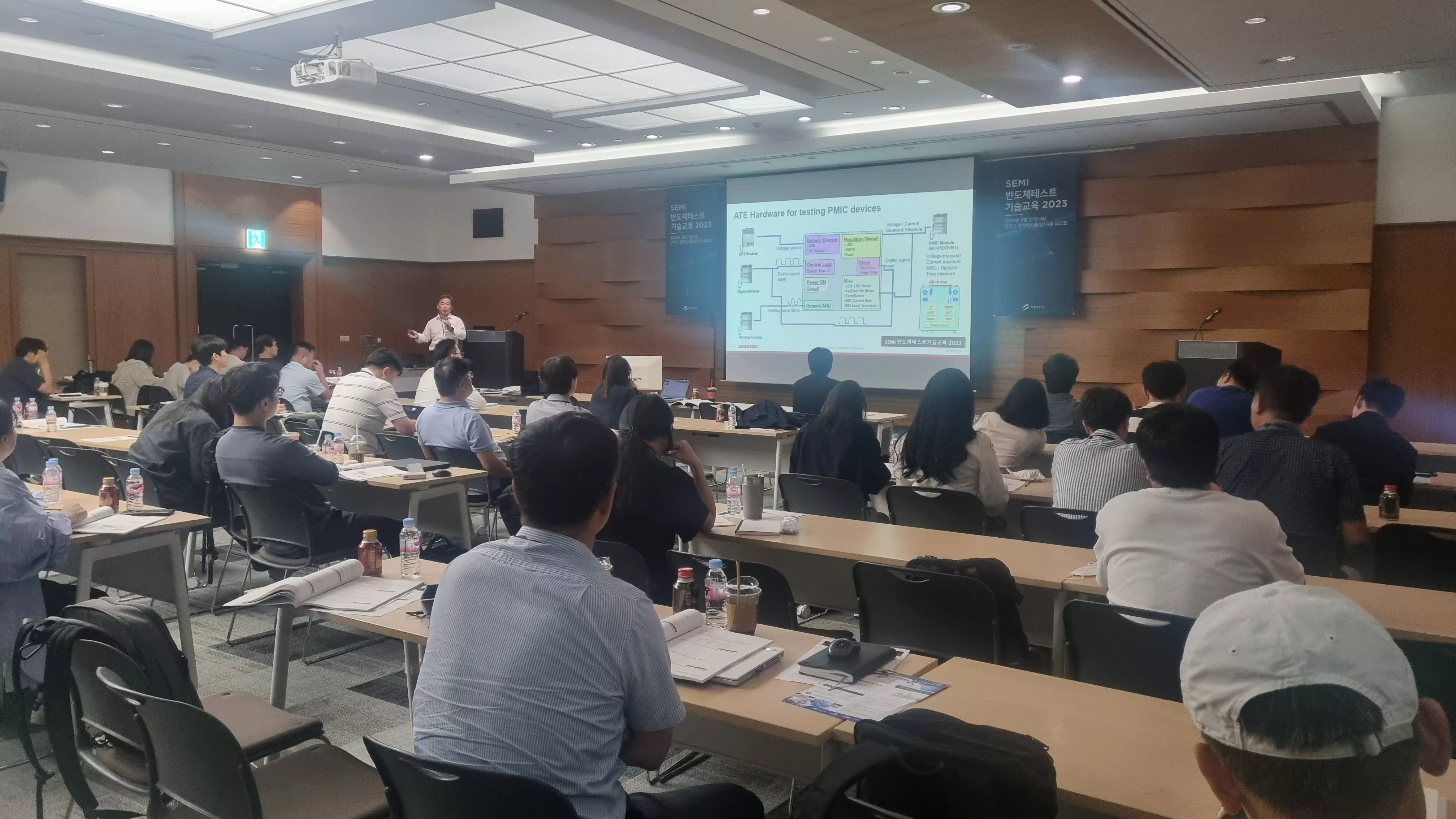
Power & Analog Test Introduction
LED driver, PMIC, BMIC, IGBT, Silicon Carbide등 Mobile, Automotive향 Power application의 전반적인 구조 및 동작을 설명하고 test에 필요한 기본적인 요소를 이해하도록 한다. 또한 이를 측정하기 위한 ATE hardware및 device의 신뢰도를 최대화할 test 방법 및 환경에 대해 설명한다.
Lunch
Mobile SOC RF Test Introduction
최근 초연결성 환경의 구축을 위해 반드시 필요한 RF device 및 marker trend 에 대해 소개하며, 최신(mmWave) 및 전통적으로 사용되고 있는 RF device 들의 test를 위해 필요한 조건 및 각각의 test 항목에 대한 이해를 통해 보다 effective 한 Test 환경 구축 방법에 대해 이해한다.
Break
Interface/ DIB/ Socket/ Prober
반도체 검사 공정의 핵심 설비중의 하나인 TESTER 성능을 손실 없이 사용하기 위해서는 Test Socket, DIB(Device Interface Board), Probe Card 등의 interface 제품의 올바른 선택과 사용은 대단히 중요하며 특히 underkill일 때의 품질 issue 또는 overkill일 때의 양품 손실 등 품질과 비용측면에서 매우 큰 영향을 끼치는 핵심 구성품이라 할 수 있다. 기초적인 기능과 동작을 이해하고 사용자 입장에서의 올바른 제품의 선택을 위해 고려해야 할 사항들과 개발자 입장에서 설계와 개발 시 우선하여 관심을 가져야 할 부분을 살펴본다.
DRAM:Wafer & Package
- Test Introduction
- Wafer Test Process Overview
- Package Test Process Overview
- Memory Test Hardware System Introduction
SEMI 반도체테스트기술교육은 DC, AC, Logic IC 기초 테스트 기술부터, 최근 크게 상용화되고 있는 모바일/IoT 관련 IC 응용 테스트 개발에 필수적인 SOC, RF, VLSI, 메모리, PMIC 테스트 기술에 대해 다루고 있습니다. 반도체 테스트 기초교육과 기업 현장에서 실제 개발되고 있는 차세대 응용기술을 소개합니다. 기존의 세미나 형태를 벗어나 실무교육 위주로 반도체 관련 분야 인력들의 실무 이해도·기술 기반 확장·커리어 향상을 지원하고, 취업 준비생에게는 반도체 테스트 엔지니어로의 전문 지식 확보와 취업 기회 확대를 지원합니다. 관심 있는 여러분의 많은 참여 부탁드립니다.