downloadGroupGroupnoun_press release_995423_000000 copyGroupnoun_Feed_96767_000000Group 19noun_pictures_1817522_000000Member company iconResource item iconStore item iconGroup 19Group 19noun_Photo_2085192_000000 Copynoun_presentation_2096081_000000Group 19Group Copy 7noun_webinar_692730_000000Path
Skip to main content
Default Banner Image

AI

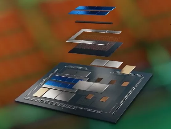
Advanced packaging is no longer operating behind the scenes. The technology of advanced packaging is helping to sustain the speed of the semiconductor industry’s improvement in power and performance, even as the Moore’s Law roadmap for wafer-level scaling comes under strain.At the Advanced Packaging Conference during SEMICON Europa 2025 in Munich, global experts examined the growth trajectory of this critical sector and Europe’s potential to lead in next-generation packaging solutions.Market Momentum Fueled by AI and HPCRomain Fraux, Chief Research Officer at Yole Group, forecasted that global revenues for advanced packaging will grow from $46.1 billion in 2024 to $79.4 billion by 2030. “Everything is linked to AI and high-performance computing (HPC),” said Fraux, while also emphasizing the growing relevance of automotive applications in driving demand.Romain Fraux, Chief Research Officer, Yole GroupThis demand is accelerating innovation across the supply chain. One emerging area is panel-level packaging, which breaks away from traditional round wafers. As Andreas Wocko, Sales Manager at Lam Research, observed, “Since the 1970s, the semiconductor industry has built on wafers. Now we are not just scaling, we are reshaping, building in a square format for the first time” – an innovation which substantially increases area efficiency and reduces device cost. Andreas Wocko, Sales Manager Europe, Lam ResearchTechnology Transformation from Lab to FabEurope is already investing in the foundational technologies that will power tomorrow’s packaging systems. Rolf Aschenbrenner, Deputy Director of Fraunhofer IZM, the home of the European Union’s APECS advanced packaging pilot line, discussed ongoing research into functional interposers, routing density, and organic interposers. “Our goal is to show how a new design philosophy incorporating chiplets can be brought to the industrial systems level,” said Aschenbrenner.Rolf Aschenbrenner, Director Deputy, Fraunhofer IZMThese breakthroughs are essential, as pitch sizes shrink and new materials emerge. Dr. Jessica Stubbe, Global Application Manager at MKS Atotech, described how interconnect densities have doubled in the past two years, with the industry moving to pitch sizes of less than 10µm. Stubbe said this new technology “will be enabled by a move from traditional solder-based interconnects to copper-to-copper hybrid bonding to provide higher density I/Os and lower resistance.” Jessica Stubbe, Global Application Manager, MKS AtotechInnovation Meets Real-World IntegrationThis increased density carries thermal risks with it. As Ram Trichur, Global Head of Semiconductor Packaging at Henkel Corporation, said, “New architectures enabled by advanced packaging are putting power devices on the backside, interposer or substrate, and this addition of more power delivery components in the package creates more local hotspots.”The reduced feature sizes inside the latest packages make it more difficult than ever to apply thermal interface materials. “At Henkel, we are now making 1µm-level fillers which enable the effective filling of gaps as small as 7µm,” said Trichur.Ram Trichur, Global Head of Semiconductor Packaging Market Segment, Henkel CorporationOne of the applications which stands to gain the most from the development of advanced packaging technology is silicon photonics. Dr. Himani Kamineni, Director for Advanced Packaging at GlobalFoundries, described how co-packaged optics (CPO) brings photonics directly inside the package, reducing connection lengths from centimeters down to millimeters, and providing higher bandwidth and lower latency at lower power. “Advanced packaging and CPO are foundational elements for AI and data centers to enable scalability to the next generation of compute,” said Kamineni. “But it will need a lot of packaging innovation: silicon interposers, copper-to-copper interconnects, and fiber-attach units for precise alignment.” Himani Kamineni, Director, Advanced Packaging, GlobalFoundriesReliability and Test Under PressureIn the transition to new packaging technology, it is crucial that the industry does not lose sight of the reliability standards which have made semiconductors so valuable in sectors such as automotive and aerospace. Amar Mavinkurve, Director of Materials and Labs Package Innovation at NXP Semiconductors, warned the finer spacing and smaller feature sizes in the latest packages posed a problem for reliability and long-term performance. He said, “We are dealing now not just with one failure mechanism, but with multiple. So, the way that we are used to describing behavior in models will not necessarily hold in future. Even industry standards might not hold.”Discussing new technologies such as copper-to-copper interconnects, Mavinkurve pointed out that failure would not be due to a single event, but to processes such as electromigration, corrosion, and thermomechanical effects. To model reliability properly in future, he said, “we need to move from a physics of failure to a physics of degradation.” Amar Mavinkurve, Director Materials and Labs Package Innovation, CTO, NXP SemiconductorsFabio Pizza, Business Segment Manager at Advantest Europe focused on quality and failure. With geometry scaling toward 1nm, early identification of known-good dies is essential to optimize cost and test coverage. Pizza said that, while device manufacturers need to keep time-to-market and the cost of test under tight control, they are also trying to figure out how to increase test coverage. “In a modern GPU, even a 100 DPPM quality process leaves 20 million transistors untested,” he said. Fabio Pizza, Business Segment Manager, Advantest EuropeEurope’s Position in the Global EcosystemThe conference concluded with a panel discussion about the prospects for Europe in the global advanced packaging market. According to Yole’s Romain Fraux, there is a strong ecosystem in Europe: “Europe’s strengths include specialized packaging service providers in the photonics and power market segments, as well as many packaging equipment manufacturers,” said Fraux. This resonated with the instincts of NXP’s Amar Mavinkurve and Advantest’s Fabio Pizza. Mavinkurve said: “We should focus on what we are already good at doing. It will be challenging to compete with advanced packaging providers elsewhere for AI and HPC business.”Ram Trichur of Henkel, however, urged the industry in Europe, “Do not take your foot off the gas on advanced packaging. You cannot do the full stack here, but in a technology such as CPO, there is a lot of innovation in Europe, and there is scope to add the manufacturing of these devices on top of the research capabilities.”Chris Scanlan, Senior Vice President of Technology at Besi, raised the idea of shifting production toward Eastern Europe. But Trichur cautioned that talent and infrastructure remain limiting factors in that strategy. From left to right: Chris Scanlan, Senior Vice President Technology, Besi;Amar Mavinkurve, Director Materials and Labs Package Innovation, CTO, NXP Semiconductors; Fabio Pizza, Business Segment Manager, Advantest Europe; Rolf Aschenbrenner, Director Deputy, Fraunhofer IZM; Ram Trichur, Global Head of Semiconductor Packaging Market Segment, Henkel CorporationCollaboration is the Path ForwardSpeakers throughout the conference echoed a common message: advanced packaging is reshaping the semiconductor landscape, and global collaboration will be essential to success. “It is impossible for one country or one region to do the entire stack,” Trichur concluded. “Innovation must be matched with strategic partnerships to bring advanced packaging from research to real-world impact.”On behalf of SEMI, the SEMI Europe team would like to thank the industry leaders whose expertise and enthusiasm made this conference a resounding success. SEMI ContactCassandra Melvin, Senior Director of Business Development and OperationsEmail: [email protected]
Read More
The semiconductor industry is undergoing a rapid transformation. Artificial intelligence (AI) applications, such as agentic and physical AI, push compute demands to unprecedented heights, prompting the semiconductor industry to push the boundaries of 2nm technology and beyond. Yet, as we move to these advanced semiconductor technology nodes, it has become increasingly challenging for academic research to remain closely connected with the fast-evolving industrial developments, limiting academic researchers in driving innovation. Europe’s NanoIC pilot line, a pioneering European initiative, hosted by imec, is addressing this challenge by offering pathfinding process design kits (P-PDKs). To cover the potential of these P-PDKs and their impact on Europe’s semiconductor ecosystem, we sat together with Professor Mehdi Tahoori (professor at Karlsruhe Institute of Technology) and Anita Farokhnejad (DTCO Program Manager at imec).SEMI: What exactly is a P-PDK, and how does it differ from traditional PDKs?Farokhnejad: At its core, a process design kit (PDK) is a software environment that enables circuit designers to simulate, validate, and optimize chip designs using realistic models of chip technology. Consider it a blueprint or a simulation toolkit allowing chip designers to explore performance, power, and manufacturability of a new chip architecture in a virtual sandbox. What sets P-PDKs apart is that they anticipate future technologies. Unlike traditional PDKs, which are based on existing technologies, P-PDKs are built on predictive models of future nodes and architectures. This allows researchers to explore system-level trade-offs, assess architectural implications, and prepare design flows before a technology reaches maturity. SEMI: Why are they so crucial for academia?Tahoori: For decades, academic researchers could contribute to semiconductor innovation using abstraction layers that allowed them to design and test new architectures without direct access to the latest technologies. This approach worked well until the industry reached the 20-nanometer node. At that point, the complexity of semiconductor design increased, with the introduction of advanced device architectures like FinFETs, nanosheets, Forksheets, CFETs, and novel integration solutions such as 3D stacking and chiplet integration.Transistor scaling in the AI eraTraditional abstraction models could no longer keep up with these advances, and the gap between academic research and industrial practice began to widen. This growing gap started to limit academia’s ability to participate in semiconductor paradigm shifts, such as CMOS 2.0 and new computing architectures. P-PDKs, enabled by the NanoIC pilot line, aim to bridge this gap, restoring the connection between academic thinking and industrial progress.SEMI: How does this support semiconductor innovation in Europe?Tahoori: Universities are ideally positioned to drive out-of-the-box innovation and invent new paradigms for computing. This is where universities truly excel. But to do that, they need access to the latest technologies and tools. We see for example a strong focus on the AI revolution and how the microelectronics industry is enabling that transformation. To meet the demands of AI applications and the computing power they require, we need to design new computing architectures based on advanced technology nodes. This is precisely the academic area of expertise. To design these new AI computing architectures, however, we need the most advanced technologies available. The P-PDKs for advanced nodes provided by the NanoIC pilot line now make this kind of research possible at universities. Something that was not feasible before.Additionally, the P-PDKs also provide an important reference technology and platform to benchmark and validate these innovations within a next-generation design roadmap. This means researchers can test their novel architectures against realistic process and performance metrics.SEMI: Are they only available for academia?Farokhnejad: The NanoIC P-PDKs are meant to be accessible to foster innovation across Europe’s semiconductor ecosystem. These advanced PDKs are therefore also available to European research organizations, startups, and industry partners. Access is facilitated through Europractice, where eligible users can apply by signing a Design Kit License Agreement (DKLA). Once approved, they gain access to the PDKs.SEMI: What other technology nodes are NanoIC’s PDKs addressing?Farokhnejad: The first P-PDK was released in June (first version of the N2) and supports frontside and backside routing with TSVM, standard cell libraries, and multiple VT flavors for early-stage design exploration. Upcoming releases include new versions of the N2 P-PDK, as well as A14 and A7 PDKs, eDRAM and SOT memory PDKs, and advanced interconnect solutions such as redistribution layers (RDL), hybrid bonding, and interposers.Those interested in learning more about the NanoIC ecosystem and the research enabled by the P-PDKs can meet representatives and partners of the NanoIC pilot line during SEMICON Europa, November 18-21 at booth C2417 in Messe Munchen. More information about the initiative is also available on the NanoIC website.BiosMehdi Tahoori, Professor Chair of Dependable Nano-Computing - Karlsruhe Institute of Technology Mehdi B. Tahoori is Professor and Chair of Dependable Nano-Computing at the Karlsruhe Institute of Technology (KIT), Germany, and guest professor at imec, focusing on CMOS 2.0 and future chip technologies. He previously worked at Xilinx (USA), Fujitsu Labs (USA), and served as a junior professor at Boston Northeastern University (USA) and as a visiting professor at the University of Tokyo (Japan). He earned his B.S. from Sharif University (Iran) and M.S./Ph.D. from Stanford (USA). Prof. Tahoori is Deputy Editor-in-Chief of IEEE Design and Test Magazine, is a former Editor-in-Chief of Elsevier Microelectronic Reliability and has chaired major IEEE symposia. His honors include multiple best paper nominations and conference awards, the US National Science Foundation Early Faculty Development (CAREER) Award (2008), an ERC Advanced Grant (2022), and an IEEE fellowship.Anita Farokhnejad, DTCO Program Manager - imec Anita Farokhnejad earned her PhD from Universitat Rovira i Virgili (Spain), specializing in FEOL and device modelling. She joined imec in 2021 as an R D Engineer, focusing on BEOL optimization and future roadmap development. Collaborating closely with integration and physical design teams, she develops models for PnR data analysis and BEOL optimization. Her recent work on the enhanced Ring Oscillator (eRO) model aids in the early assessment of new materials and BEOL boosters. In August 2023, she advanced to team lead for PDK Enablement, translating advanced semiconductor nodes into Pathfinding-PDKs. Farokhnejad is also dedicated to education, conducting courses that make sophisticated technological concepts accessible to both industry veterans and aspiring engineers. Currently, she serves as Program Manager of DTCO at imec, where her contributions continue to drive innovation in the semiconductor industry.AcknowledgementThis work was enabled by the NanoIC pilot line. The acquisition and operation are jointly funded by the Chips Joint Undertaking, through the European Union’s Digital Europe (101183266) and Horizon Europe programs (101183277), as well as by the participating states Belgium (Flanders), France, Germany, Finland, Ireland and Romania. For more information, visit https://www.nanoic-project.eu.DisclaimerFunded by the European Union. Views and opinions expressed are however those of the author(s) only and do not necessarily reflect those of the European Union or Chips Joint Undertaking. Neither the European Union nor the granting authority can be held responsible for them. SEMI ContactJames Lam, Business Development ManagerEmail: [email protected]

Read More
With increasing demand for personalized smart devices, the MEMS and sensor market is undergoing rapid transformation. MEMS sensors are the backbone of smart wearable devices, seamlessly integrating multiple functions to monitor and simplify our day-to-day activities. As applications in healthcare, environmental tracking, and AR/VR expand, the need for ultra-compact, energy-efficient, and intelligent sensors is more critical than ever.In an exclusive conversation with SEMI, Stefan Finkbeiner, CEO of Bosch Sensortec, shared his perspective on the dynamic landscape of MEMS sensor technology. From Bosch’s evolution to a solutions provider with a focus on sustainability and market-driven innovations, Finkbeiner offered a deep dive into how Bosch Sensortec is positioning itself at the forefront of the industry. “We have to think in terms of the end application and determine what the right hardware and software configuration should be in order to provide solutions with the greatest benefit and flexibility.”Further insights into the future of MEMS and sensor technology will be shared by Finkbeiner during his keynote at the SEMI MEMS Imaging Sensors Summit on November 14, 2024, in Munich, Germany. Registration is still open.SEMI: Welcome, Stefan, and thank you for sharing your insights on advanced sensor technologies. Let’s start with a personal question: What motivates and inspires you about working in sensor technology?Finkbeiner: Sensor technology is very diverse and has significant impacts on consumers. We take pride in prioritizing consumers’ needs and benefits. True to the Bosch motto, “Invented for life,” we are committed to making life better, easier and healthier. This is demonstrated in our sensing solutions, which provide valuable data for fitness tracking in smartwatches, enhance the audio experience in hearables, and enable real-time monitoring of air quality to help individuals make informed decisions for a healthier environment. I am fascinated by technology advancements that are enabling the scaling of sensors—and the processing power and intelligence packed into these increasingly compact devices. For instance, our latest acceleration sensors for hearables are the smallest in the world and are nearly invisible at just 1.2 x 0.8 x 0.55 mm³.We leverage innovative wafer level chip scale packaging (WLCSP) to achieve this reduced form factor. These compact, feature-rich, high-performance accelerometers are easier to integrate in the latest generation consumer products where size and functionality are critical requirements.SEMI: How has Bosch Sensortec’s approach evolved over the years and what is the company’s primary focus today? Finkbeiner: We began our success story a few years ago as a hardware supplier, with one of our first applications being the 'Portrait-Landscape' function in smartphones. Over time, we’ve evolved into one of the leading providers of MEMS sensors.Today, we no longer see ourselves purely as a sensor manufacturer, but as a technology solutions provider. Our focus has shifted to think in terms of the end application and determine what the right hardware and software configuration should be to provide solutions with the greatest benefit and flexibility.Achieving this requires significant software and artificial intelligence (AI) development. In essence, we are optimizing software through self-learning models. Hardware remains essential for optimizing power consumption, with most sensors integrating a controller alongside the ASIC to enable seamless software integration.This unique software and hardware configuration unlocks exciting possibilities and broadens our market reach. We see significant growth in head-mounted devices, and we are actively working on related acoustics solutions.SEMI: Looking ahead, what trends do you anticipate will have the most significant impact on the MEMS sensors market?Finkbeiner: We see several trends that will significantly impact the MEMS sensor market. First, there is growing demand for personal health monitoring in consumer and mobile electronics. Wearable devices, in particular, are becoming essential tools for individuals to track their health and fitness status. This trend requires MEMS sensors to become even more accurate, with solutions that include sophisticated software algorithms to ensure reliability, accuracy, and reproducibility. As a result, AI and machine learning (ML) technologies will play a crucial role in enhancing sensor performance.A second important trend is the continued miniaturization of MEMS sensors. To meet customer demands, sensors must integrate more functionality, including edge-processing capabilities. For example, what once may have been a simple accelerometer with a step-counting algorithm is now evolving into a 6-axis Inertial Measurement Unit (IMU) with an integrated microcontroller and advanced AI/ML software. A great example of this is in True Wireless Stereo (TWS) earphones, where the IMU not only tracks steps but also enables complex tasks like dead reckoning and supports 3D audio—all within the tight constraints of a small TWS earbud housing. Low power consumption, as always, is a critical factor for these mobile devices to meet CE (Conformité Européenne) standards.Finally, we believe that smart glasses, augmented reality (AR) and virtual reality (VR) devices are poised to become the “next big thing.” These devices require advanced image projection optics that offer excellent optical quality, low weight, and ease of use to ensure consumer adoption. We believe our MEMS-based LBS (Laser Beam Scanning) solution is ideal for these applications. Additionally, the successful adoption of smart glasses hinges on high-performance MEMS sensors that are compact, accurate, and power-efficient—critical requirements for all-day wearability and functionality.These trends underscore the need for MEMS technology to evolve, integrating greater functionality, precision, and efficiency to meet the demands of next-generation consumer devices.SEMI: What are some of the biggest challenges facing the MEMS sensors industry today, and how can companies overcome them?Finkbeiner: One key challenge is that the smartphone market—arguably the most attractive market for a variety of MEMS and MOEMS sensors—has become more or less saturated. To stay competitive, MEMS companies must innovate existing products while also developing new, differentiated sensors and actuators for next-generation mobile products.SEMI: How is Bosch Sensortec supporting sustainability initiatives?Finkbeiner: We are helping to mitigate climate change with our low carbon footprint solutions.Up to 20% of annual global carbon emissions are caused by forest fires. This is equivalent to carbon dioxide emitted by all the vehicles driven worldwide. Our sensors can detect forest fires before they develop into wildfires by measuring various gases such as carbon monoxide and hydrogen. In parallel, we are working with our production partners to reduce our carbon footprint over the coming years, while also replacing or minimizing the use of environmentally hazardous chemicals, such as PFAS.SEMI: What are you most excited about for the MEMS Imaging Sensors Summit, and how do you think it will impact the European semiconductor industry?Finkbeiner: The European semiconductor industry has deep expertise in MEMS and sensor technologies, positioning it to make a significant impact in markets such as consumer health, optical sensing, and AR displays. By continuing to focus on sustainable solutions, we can drive even greater impact for the broader industry and secure Europe’s leadership in these growth sectors.I look forward to collaborating with industry peers at the Summit to define next steps needed to advance Europe’s leadership. The MEMS Summit is an invaluable opportunity to collaborate and drive progress, and I warmly invite my colleagues to join us in shaping the future of the European semiconductor industry.Dr. Stefan Finkbeiner Dr. Stefan Finkbeiner has been CEO and General Manager at Bosch Sensortec GmbH since 2012. He was born in 1966 in Freudenstadt, Germany. Stefan Finkbeiner held various senior positions at Bosch including Director of Sensor Marketing, Director of Corporate Research in microsystems technology, and Vice President of Sensor Engineering. He looks back on almost 30 years in semiconductor industry working in different positions related to sensor research, development, manufacturing, and marketing. Due to his wide experience in semiconductor and sensor industry, Stefan Finkbeiner is a recognized guest in panel discussions and as keynote speaker. SEMI ContactSitong He / Communications Manager, SEMI EuropeEmail: [email protected]: +49 151 5546 2638
Read More
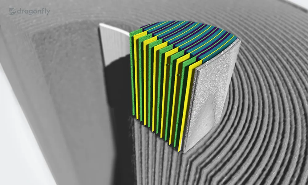
In today’s rapidly evolving semiconductor industry, ensuring both precision and efficiency in manufacturing has become an increasing challenge, particularly as advanced technologies like MEMS and AI chips push the boundaries of design and production. Inspection methods that were once sufficient are now falling short, making room for cutting-edge solutions powered by artificial intelligence (AI). The introduction of AI-driven 3D X-ray inspection technologies is transforming the landscape, offering manufacturers a sophisticated tool to ensure quality control, while driving sustainable production strategies.SEMI spoke with, Joscha Malin, Product Manager, and Daniel Stickler, R D Expert for X-ray Imaging at Comet AG, Industrial X-Ray System Division, to explore how AI-powered 3D X-ray inspection technologies are shaping manufacturing. They delve into how these technologies address critical challenges during inspections and defect analysis, using tools such as Dragonfly 3D World software for user-friendly, AI-driven insights that facilitate effective decision-making.Further insights into the application of AI-powered 3D X-ray inspection technologies and their role in advancing MEMS manufacturing will be presented by Stickler at the SEMI MEMS Imaging Sensors Summit on November 14, 2024, in Munich, Germany. Registration is now open.SEMI: Thank you both for agreeing to share your insights. To start, can you explain the importance of inspection strategies in the context of MEMS manufacturing?Malin: As MEMS devices become increasingly miniaturized and complex, effective inspection strategies are crucial. These strategies not only accelerate the wrap-up of production processes, but also significantly enhance product yield. With tighter tolerances and various materials involved, ensuring the integrity and functionality of each component is more critical than ever. A robust inspection strategy allows us to catch potential defects early, which can save time and costs associated with rework or scrap.Stickler: The evolution of MEMS technology, particularly in AI chips, demands a higher level of inspection sophistication. Traditional methods may fall short in providing the necessary detail and speed, which is why we’re focusing on advanced solutions like our AI-powered 3D X-ray inspection.SEMI: Could you elaborate on how the 3D X-ray technology differs from conventional inspection methods? Stickler: The 3D X-ray technology we utilize acts as a bridge between traditional optical methods and standard 2D X-ray inspection. It offers high-resolution, three-dimensional images without damaging the samples. 3D X-ray technology emphasizes three main benefits: clarity, efficiency, and actionable insights. This means we can obtain detailed images that help us analyze components more effectively, allowing for real-time decision-making.Malin: Moreover, the clarity and detail provided by the 3D X-ray images are critical when it comes to defect analysis in MEMS devices. They allow us to assess mechanical, electrical, and assembly errors in ways that conventional methods simply cannot. This leads to a more reliable production process.SEMI: What specific MEMS defects can be effectively analyzed using this technology?Stickler: There are several types of defects we can analyze. For instance, we can detect mechanical defects such as stiction or fractures, as well as electrical failures like short circuits. The 3D X-ray inspection allows us to visualize these defects in detail. Additionally, we can monitor assembly errors, which are particularly important in complex MEMS devices where misalignments can lead to significant issues.Malin: I’d like to add that early detection of these defects is paramount. The faster we identify issues, the quicker we can implement corrective actions, thereby improving overall yield and reducing production costs.SEMI: You mentioned yield improvement earlier. Can you explain how your technology contributes to that?Malin: Our approach supports process optimization by providing information on product characteristics and, for example, allows us to identify trends early on that may lead to yield issues later. We also aim to accelerate new product introduction in the early phase by rapid feedback, saving time and cost. This is crucial because many defects may not be apparent until later stages of production. With our technology, we can monitor samples in real-time, allowing us to react promptly to emerging challenges.Stickler: By integrating this feedback loop, we can significantly shorten the time to market for new products. This is particularly beneficial in industries where speed and efficiency are essential.SEMI: Can you tell us about Dragonfly 3D World software and its role in this process?Malin: Dragonfly 3D World is a user-friendly software that leverages AI and, specifically, deep learning for image processing. It enables users to efficiently perform bump metrology and defect identification, for example, without needing extensive expertise in the field. The software makes complex processes manageable, even for operators who may not be specialists in image processing.Stickler: Beside MEMS and advanced packaging in GPU production, this software is indeed an “AI-for-AI” application. By utilizing deep learning, users can train models that adapt to various imaging tasks, making the entire inspection process more efficient. The insights generated from the 3D X-ray images are automated, enhancing usability and streamlining workflows.SEMI: In conclusion, what are the key takeaways you’d like to share?Malin: The key takeaways are that AI-driven 3D X-ray inspection is transformative for the MEMS manufacturing process, enhancing inspection strategies and defect detection significantly. By integrating advanced technologies, we can ensure higher product quality and efficiency.Stickler: Yes, and I would emphasize the importance of powerful monitoring and non-destructive test tools. Our innovative solutions not only improve yield, but also pave the way for sustainable practices in manufacturing, ultimately benefiting the industry. Dr. Daniel SticklerDirector X-ray Technology Components at Comet AG, Industrial X-Ray System Division. Based in Hamburg, Germany, he holds a PhD in Physics from the University of Hamburg and has extensive experience in X-ray imaging, semiconductor X-ray applications and product innovations. Joscha MalinDirector Product Marketing Software Products at Comet AG, Industrial X-Ray System Division. Based in Hamburg, Germany, he holds a degree in Electrical Engineering with specialization in Semiconductors and profound experience in the industry. For over a decade, he has focused on developing X-ray inspection and metrology solutions, especially for the Semiconductor industry. SEMI ContactSitong He / Communications Manager, SEMI EuropeEmail: [email protected]: +49 151 5546 2638
Read More