downloadGroupGroupnoun_press release_995423_000000 copyGroupnoun_Feed_96767_000000Group 19noun_pictures_1817522_000000Member company iconResource item iconStore item iconGroup 19Group 19noun_Photo_2085192_000000 Copynoun_presentation_2096081_000000Group 19Group Copy 7noun_webinar_692730_000000Path
Skip to main content
Default Banner Image

Workforce Development

This blog series explores how collaboration between industry and academia can empower the next generation of semiconductor innovators. Through insights from leaders, educators, and students, we’ll showcase effective strategies for bridging the talent gap, fostering innovation, and creating meaningful career pathways in the semiconductor industry.As innovation accelerates and new challenges emerge, the industry’s greatest breakthroughs will come from bold, curious students, young professionals, and lifelong learners ready to build what comes next. SEMI spoke with Professor Antonio Costa of the University of Catania about attracting the next generation to STEM, the emerging skills required in the semiconductor industry, and examples of impactful collaboration with local industry, along with many other insights.Costa shared his perspectives following his participation in the SEMI on Campus program, held on April 16, 2026, in Catania, Italy. SEMI: What emerging skills do you believe will be most essential for the next generation of semiconductor innovators, and how can industry and academia work together to nurture them?Costa: I firmly believe in the role of interdisciplinary skills. The next generation of semiconductor innovators will need a blend of deep technical expertise, cross-disciplinary thinking, and adaptability to rapidly evolving technologies specifically based on artificial intelligence. The future semiconductor innovator isn’t just a circuit designer. They’re a systems thinker, data scientist, and materials engineer rolled into one. The most successful ecosystems will be those where academia teaches fundamentals, and industry provides real-world constraints, tools, and scale. So, university and industry should work together to share their knowledge and technological infrastructures with the aim of supporting the next generation of semiconductor innovators. SEMI: In your work with young engineers and researchers, what approaches have you found most successful in nurturing creativity and sustaining curiosity in such a technically complex field? How do you think we can attract the next generation to enter the STEM studies?Costa: Curiosity and creativity are two major features for researchers and engineers in general. Over the years of teaching and coordinating research activity, I have been able to observe that students are increasingly drawn to challenges coming from the industrial world. In a way, one could say that complexity often stimulates curiosity, and when this happens, students are able to deliver their best performance in terms of creativity and quality of results. In my courses, students have always been required to tackle an industry-inspired project work to be eligible to pass the exam. Every year, I invite industry representatives from local manufacturing companies to present real case studies to the classroom, describing their key elements, constraints, and objectives. Students are then asked to solve the industrial case study by applying the problem-solving techniques learned during the course. Based on my experience, I believe that a greater intensity in the relationship between the industrial and academic worlds can further stimulate students' curiosity and the interest of new generations.SEMI: What do you believe are the most significant barriers for students entering the semiconductor industry today, and how can academia help bridge these gaps?Costa: As usual, the main barriers for students concern the gap between the theoretical study mindset developed during university courses and the demands of the industrial world in terms of teamwork skills, problem-solving abilities, and soft skills. Universities and industry should find greater opportunities for collaboration, for example by establishing shared laboratory activities or seminars during which managers from semiconductor companies, and beyond, illustrate the essential aspects of working life and the primary needs of the semiconductor industry. At the same time, it would be advisable to emphasize the employment and career opportunities that the semiconductor industry is currently able to offer. Hackathons, that have a competitive orientation, could also represent a valid stimulus that companies and universities could pursue jointly and on a regular basis.SEMI: How can universities and industry partners collaborate more effectively to create learning experiences that truly unlock students’ potential and prepare them for the sector’s evolving demands? Professor Antonia Costa, University of Catania and Daniele Pagano, STMicroelectronicsCosta: Shared laboratories, curricular and extracurricular internships scheduled on a continuous basis, and periodic seminars held by company representatives with diverse areas of expertise can make a positive contribution to rapidly and robustly unlocking the learning potential of today's students and tomorrow's new hires. In December 2021, the University of Catania and STMicroelectronics signed a framework agreement to strengthen collaboration in the field of power electronics, with a focus on advanced research and training. The agreement aims to support technological innovation and the development of professional skills in the semiconductor sector, including:Research and development: the launch of projects focusing on increasing power density, efficiency, and reliability of power modules. Training and talent: funds for students’ awards, mentorship programs, internships, thesis projects.Innovation: support for technological growth and the development of professional expertise in power electronics. Regional ties: consolidation of Catania's role as a hub for semiconductor research, with strong synergy between the university and the local ST production site. Curricular internships linked to Master’s degree theses, supervised by faculty members across disciplines, primarily within Engineering, Computer Science, Physics, and Chemistry programs.SEMI: Can you share other examples of collaborations? Costa: Over the past decade, the University of Catania has been an active partner in multiple European consortia, supporting the development of research projects funded through highly competitive national and European programs. Currently, the University of Catania is engaged in collaborative research with STMicroelectronics through two Horizon Europe projects.In the first project, HiCONNECTS, the Department of Engineering is developing a digital twin architecture aimed at optimizing wafer lot dispatching at STMicroelectronics’ manufacturing facility in Catania.The second project, GENESIS, brings together the Department of Engineering and the Department of Chemical Sciences to pursue an ambitious sustainability objective: the development of innovative methods to identify and reduce per- and polyfluoroalkyl substances (PFAS) generated by semiconductor manufacturing processes, thereby mitigating environmental impact."The role of universities is to help students recognize their potential and guide them toward fields where their abilities can truly flourish. Initiatives like SEMI on Campus are invaluable, as they inspire students through direct engagement with professionals, helping bridge the gap between theory and industrial practice." -- Professor Antonio Costa, University of Catania .custom-quote-block { border-left: 4px solid #d9d9d9; padding-left: 26px; margin: 24px 0; } .custom-quote-block blockquote { margin: 0; padding: 0; border: none; } .custom-quote-block p { margin: 0; font-size: 18px; line-height: 1.6; font-style: italic; color: #000; } SEMI: Looking ahead, what role do you see educators playing in shaping the future of semiconductor innovators? Costa: The role of educators, both in schools and, above all, in universities, is to help students recognize their own potential and develop the maturity needed to identify and pursue those fields of knowledge that best highlight their abilities.The SEMI on Campus initiative was immediately embraced by many universities and by myself, as it offers students from diverse academic backgrounds the opportunity to understand the key skills sought by players in the semiconductor industry, while also highlighting the employment and career paths available in this field.The opportunity to hear directly from prominent speakers who work daily in semiconductor design and manufacturing represents a powerful way to stimulate students’ curiosity and potential, while helping to bridge the gap between the theoretical knowledge acquired in university classrooms and the practical, results‑oriented approach required in an industrial environment.The benefits for students are broad and significant, as they can assess their own aptitudes and ambitions against the real demands of semiconductor companies, drawing inspiration and insight from firsthand accounts shared by industry professionals.Antonio Costa is a full professor at the University of Catania (DICAR Department). He teaches Production Planning and Control in the Master’s degree in Engineering Management, and Advanced Technologies for Manufacturing Processes in the Master’s degree in Mechanical Engineering.His research activities are mainly focused on production scheduling, supply chain dynamics, manufacturing process optimization and Statistical Process Control (SPC). He is area editor for Computers Industrial Engineering, member of the Italian Association of Manufacturing Technologies (AITeM) and leads several research collaborations with STMicroelectronics.Interested in bringing SEMI On Campus to your institution or welcoming an industry expert as a guest speaker?Reach out to [email protected]. Let’s work together to inspire the next generation of semiconductor leaders!Related Initiatives:SEMI 20 Under 30: The SEMI 20 Under 30 Awards recognize exceptional young leaders in the semiconductor industry who are making significant contributions and driving innovation. Nominations are open!ChipQuest: The ChipQuest Challenge promotes the microelectronics industry to students to build future talent. University and high school students can participate and win amazing prizes! Serena Brischetto is Director Marketing and Digital Engagement at SEMI Europe.
Read More
The Rising Stars: 20 Under 30 blog series celebrates the brightest young leaders shaping the future of the semiconductor industry. These exceptional individuals have earned the SEMI Europe 20 Under 30 Award for making a remarkable impact across the supply chain—whether in engineering, sales, marketing, or R D. Nominations for the 2026 20 Under 30 Award are now open, providing the opportunity to recognize and honor the next wave of industry trailblazers.The series spotlights these rising stars for their career achievements, commitment to innovation, leadership skills, and dedication to driving both business success and community growth.Follow their inspiring journeys and discover how they are thriving and paving the way for future generations in the semiconductor world.Meet Pascal Fasel, Project Manager Engineering at Comet X-rayPascal Fasel’s career in semiconductors has developed steadily through hands-on experience and continuous learning. Starting with an apprenticeship in 2012, he built his foundation across design, process, and project roles, gaining a practical understanding of how technologies move from concept to production.Over time, he discovered a strong interest in solving real-world problems and delivering reliable engineering solutions. Today, as Project Manager Engineering at Comet X-ray, Fasel focuses on guiding projects through complexity while balancing speed, precision, and quality in a fast-evolving industry. SEMI: What inspired you to join the semiconductor industry? Fasel: I did not have a single defining moment. I joined through an apprenticeship in 2012 and discovered semiconductors gradually. As my responsibilities grew, I realized that I enjoy solving problems and turning ideas into reliable solutions. Over the past three years, I have mainly worked on semiconductor projects, which confirmed this interest. I am motivated by the fast pace, the need for precision and quality, and the impact of bringing new technology into production. It is this combination that keeps me engaged.SEMI: How did your early experiences and education shape your career path?Fasel: My apprenticeship taught me hands-on skills and the importance of quality and safety. Working across design, process, and project roles helped me understand how systems fit together and where problems arise. I am currently studying industrial engineering part-time while working. My studies and work reinforce each other, with theory supporting practice and projects testing what I learn. These experiences keep me focused on preparing technology for production.SEMI: Can you share a professional accomplishment you’re most proud of, and explain why it’s significant to you?Fasel: The accomplishment that matters most to me is my steady growth at Comet. Since joining in 2012, I have worked across design, process, and project roles. Staying for over a decade has been less about titles and more about trust, learning, and supporting colleagues when challenges arise. This is important to me because it reflects consistency and shared responsibility. It has allowed me to contribute to projects from idea to production in a reliable way.SEMI: As a young professional in the industry, what is your greatest challenge? Fasel: My greatest challenge is balancing speed with quality in a changing environment while ensuring smooth handovers to production. Specifications can change, results can be unexpected, and timelines can shift. To manage this, I focus on learning quickly without cutting corners. I make changes small and reversible, identify risks early, and seek feedback regularly. The goal is to learn efficiently and reduce surprises. SEMI: What advice would you give to younger generations aspiring to make an impact in this industry?Fasel: Stay curious and build a habit of learning every day. You will not master everything at once. Projects move quickly, so remain flexible and start with small steps. Gain experience early through internships or student projects. Apply what you learn in practice. Ask clear questions, listen carefully, and stay open to different perspectives. Share credit when things go well and take responsibility when they do not. Be patient. Steady progress is more effective than big jumps. Focus on quality and safety, even under pressure, and build trust through consistency.SEMI: How do you envision future work environments?Fasel: I believe workplaces will become more flexible and people-focused. Clear goals, open communication, and early feedback will be essential. Collaboration will be hybrid, with time in the office used when it adds value. Teams will focus more on outcomes rather than hours, working in small, manageable steps to reduce risk and stay aligned.SEMI: What impact has the 20 Under 30 Award had on your career? Fasel: I am grateful for the recognition. It has not changed my daily work, but it has created opportunities to connect with others, learn from peers, and share experiences. It also provides a platform to encourage students and early-career professionals to explore this industry. For me, it is a reminder to stay consistent and continue supporting others.Following 20 Under 30 JourneysPascal Fasel’s story reflects the value of persistence, practical experience, and continuous improvement. His work highlights how steady progress and collaboration contribute to delivering reliable semiconductor solutions.The Rising Stars: 20 Under 30 blog series celebrates the exceptional talent and leadership driving the future of the semiconductor industry. Each of the young innovators honored is excelling in their respective fields while shaping the landscape of technology and business with their visionary approaches and dedication. Their stories exemplify the remarkable achievements and unwavering commitment that define the next generation of industry leaders. The series is intended to inspire and motivate future professionals to pursue their passions and embrace the opportunities within this dynamic industry. Stay tuned for more stories of rising stars who are paving the way for continued growth and innovation in the semiconductor world.Learn more about the SEMI Europe 20 Under 30 Award and the recipients honored at SEMICON Europa. If this is of interest and you would like to explore further workforce related topics, we invite you to learn more about ChipQuest. SEMI ContactJames Lam, Business Development ManagerEmail: [email protected]
Read More
The Rising Stars: 20 Under 30 blog series celebrates the brightest young leaders shaping the future of the semiconductor industry. These exceptional individuals have earned the SEMI Europe 20 Under 30 Award for making a remarkable impact across the supply chain—whether in engineering, sales, marketing, or R D. Nominations for the 2026 20 Under 30 Award are now open, providing the opportunity to recognize and honor the next wave of industry trailblazers.The series spotlights these rising stars for their career achievements, commitment to innovation, leadership skills, and dedication to driving both business success and community growth.Follow their inspiring journeys and discover how they are thriving and paving the way for future generations in the semiconductor world.Meet David Coenen, Senior Researcher at imecFrom an early curiosity about how things work to leading advanced research in photonics and thermal management, David Coenen has built his career around understanding and improving complex technologies. His interest in engineering first led him to study aerospace engineering, where he was introduced to nanotechnology and semiconductor systems. What initially seemed abstract gradually became an area he wanted to explore in depth.This growing interest led him to pursue a PhD, where he developed a strong foundation in semiconductor research. Today, Coenen contributes to advancing technologies that support high-performance computing, data centers, and AI applications, working at the intersection of multiple disciplines to address some of the industry’s most demanding challenges. SEMI: What inspired you to join the semiconductor industry? Coenen: I’ve been fascinated by technology for a long time. Ever since I was little, I’ve been eager to learn how things work, from machines to cars and airplanes. This motivated me to study aerospace engineering. During my studies, nanotechnology and semiconductors kept appearing. At first, it felt almost like magic that a piece of silicon could run complex programs. Over time, I developed a deeper understanding and wanted to explore research further. In Belgium, imec is a well-known R D institute, and I decided to pursue a PhD there to give my career a strong foundation. I also believe the semiconductor industry will have a major impact on the future of society, and I want to contribute to that.SEMI: How did your early experiences and education shape your career path?Coenen: When I was around nine or ten years old, I visited imec during a school trip and learned about computer chips. That experience stayed with me. Later, during my engineering studies, I was mentored by teachers who were passionate about science and technology. Their guidance encouraged me to push my boundaries and try things outside of my comfort zone.SEMI: Can you share a professional accomplishment you’re most proud of, and explain why it’s significant to you?Coenen: I received the Best Paper Award for a conference paper submitted to iTherm and was later awarded the Harvey Rosten Award for Excellence for the same work. This is particularly meaningful to me because the initial draft received very negative feedback. I was told it was not innovative enough and advised not to submit it to my preferred conference. From this experience, I learned an important lesson: know your worth and do not assume someone is right simply because they have more experience.SEMI: As a young professional in the industry, what is your greatest challenge? Coenen: I work in photonics and chip thermal management, which is a rapidly evolving field. Keeping up with the latest technologies and developments can be challenging. These chips are used in data centers and large AI and machine learning systems, which are in high demand. Another challenge is finding master’s or Ph.D. students to join my work. My research sits at the intersection of electronics, photonics, thermodynamics, and machine learning, which makes it highly specialized. SEMI: What advice would you give to younger generations aspiring to make an impact in this industry?Coenen: Rome was not built in one day. Developing skills and building a deep understanding of complex technologies takes time. Enjoy your studies and choose something you are passionate about. When you are passionate, learning becomes enjoyable. Think about how you want to impact the world and make it a better place. That gives you strong motivation to work hard. SEMI: How do you envision future work environments?Coenen: From my experience, having flexibility in how I plan my day and organize my work helps reduce stress. Not having a rigid schedule allows me to take breaks and reset my mind. Combined with hybrid working, this makes work more enjoyable and sustainable.SEMI: What impact has the 20 Under 30 Award had on your career? Coenen: I was very honored to receive this award. There are many researchers equally deserving, which makes it even more meaningful. The award allowed me to connect with people inside and outside my organization whom I would not normally interact with. It also increased my visibility and associated my name with excellence.Following 20 Under 30 JourneysDavid Coenen’s story highlights the curiosity, resilience, and commitment to excellence that define the next generation of semiconductor researchers. His work contributes to advancing technologies that support the growing demands of data processing and AI systems.The Rising Stars: 20 Under 30 blog series celebrates the exceptional talent and leadership driving the future of the semiconductor industry. Each of the young innovators honored is excelling in their respective fields while shaping the landscape of technology and business with their visionary approaches and dedication. Their stories exemplify the remarkable achievements and unwavering commitment that define the next generation of industry leaders. The series is intended to inspire and motivate future professionals to pursue their passions and embrace the opportunities within this dynamic industry. Stay tuned for more stories of rising stars who are paving the way for continued growth and innovation in the semiconductor world.Learn more about the SEMI Europe 20 Under 30 Award and the recipients honored at SEMICON Europa. If this is of interest and you would like to explore further workforce related topics, we invite you to learn more about ChipQuest. SEMI ContactJames Lam, Business Development ManagerEmail: [email protected]
Read More
As Europe’s microelectronics industry enters a new era of growth, one question stands out: do we have the talent pipeline to match our ambitions? The European Chips Skills Academy (ECSA), coordinated by SEMI Europe, is addressing this challenge through coordinated action, insightful research, and strong collaboration between industry and academia. Why Talent and Skills Matter The semiconductor sector in Europe is undergoing rapid transformation, driven by the European Chips Act and large-scale investments in design, manufacturing, and packaging. This momentum creates significant demand for engineers, technicians, and specialists across the electronics value chain.However, Europe faces a growing structural challenge. An ageing workforce, modest growth in technical graduates, and limited public awareness of semiconductor careers are widening the talent gap.The ECSA Skills Strategy 2024, published in November 2024, provides a detailed overview of this situation. The updated Skills Strategy 2025, released in November 2025, reinforces the urgency with new data and recommendations.According to the latest report, around 30% of Europe’s current semiconductor workforce will retire by 2030, while the inflow of graduates is increasing by less than 1% per year. This creates an annual shortfall of approximately 10,800 skilled professionals across the European value chain. Read the full report, available to download on the ECSA website.Without decisive action, this shortfall could limit Europe’s ability to meet its strategic goals in semiconductors, electronics, and digital technologies.What is European Chips Skills Academy (ECSA)?ECSA connects industry, academia, training providers, and policymakers to create a sustainable and inclusive skills ecosystem for the electronic components and systems (ECS) sector.Its core objectives are:To attract new talent into semiconductor and ECS careers.To upskill and reskill professionals for emerging roles.To build a long-term, future-ready talent pipeline across Europe.Through this initiative, SEMI Europe is leading the conversation on talent and skills, turning awareness into action and strategy into measurable results.Key ECSA Initiatives:1. ECS Summer School The annual ECS Summer School invites STEM students from across Europe to explore careers in microelectronics through lectures, workshops, and hands-on learning.The 2024 edition took place in Bertinoro, Italy, while the 2025 edition was hosted by the Budapest University of Technology and Economics in August 2025, under the theme “Fascinating Electronics for a Cool World.”The 2026 edition will return to Bertinoro, Italy on August 23-26. These events give students a first-hand look at the semiconductor ecosystem, helping them connect with experts and understand how their studies translate into real-world careers.Read more about the 2025 Summer School.2. “Day in a Fab” WebinarsThe “Day in a Fab” series offers students and young professionals the opportunity to interact directly with experts from semiconductor fabs, design houses, and equipment manufacturers.These webinars provide practical insights into various career paths within the ECS industry, helping participants better understand the range of opportunities beyond traditional engineering roles.By bridging the gap between academia and industry, these sessions help students envision a future within the European semiconductor ecosystem.See upcoming events on the ECSA website.3. Skills Strategy ReportsECSA’s Skills Strategy Reports (2024 and 2025) form the backbone of Europe’s talent development roadmap.They provide:Quantitative forecasts of job demand, workforce needs, and potential skill shortages.Insights from over 130 industry and academic experts.Recommendations for training, mobility, and reskilling programmes.The 2024 Skills Strategy Report can be accessed here, while the 2025 update is available here.These reports help policymakers, companies, and educators align their efforts to strengthen Europe’s competitiveness and ensure a resilient talent ecosystem.SEMI Europe’s Leadership in Talent and SkillsAs the global industry association for electronics manufacturing and design, SEMI Europe plays a central role in addressing the talent challenge.Through ECSA, SEMI Europe:Validates industry needs to ensure training and education are aligned with real-world demand.Connects universities and training providers with semiconductor companies to co-develop curricula.Promotes visibility and inclusion across the ECS community.Supports mobility and collaboration to create a Europe-wide approach to skills development.This leadership transforms the skills agenda from a background issue into a strategic pillar of Europe’s semiconductor ecosystem.Looking AheadThe European semiconductor industry is entering a decisive decade. The technology and investment potential are enormous, but they depend on a skilled and motivated workforce.ECSA’s work from the Skills Strategy reports to the Summer School and student engagement activities is creating a structured, evidence-based approach to developing that workforce.The path forward is clear: attract, train, and empower the next generation of engineers and innovators. With SEMI Europe’s guidance, the European Chips Skills Academy is ensuring that Europe’s ambitions in chips and microelectronics are matched by the people who will make them possible.The European Chips Skills Academy (ECSA) is a pan-European initiative coordinated by SEMI Europe and co-funded by the European Education and Culture Executive Agency (EACEA) under project number 101110124.Learn more about ECSA’s mission.SEMI ContactJatin Mendiratta, Communication CoordinatorEmail: [email protected]
Read More
The Rising Stars: 20 Under 30 blog series celebrates the brightest young leaders shaping the future of the semiconductor industry. These exceptional individuals have earned the SEMI Europe 20 Under 30 Award for making a remarkable impact across the supply chain—whether in engineering, sales, marketing, or R D. Nominations for the 2025 20 Under 30 Award are now open, providing the opportunity to recognize and honor the next wave of industry trailblazers.The series spotlights these rising stars for their career achievements, commitment to innovation, leadership skills, and dedication to driving both business success and community growth.Follow their inspiring journeys and discover how they are thriving and paving the way for future generations in the semiconductor world.Meet Anne-Mary Yeboah, Technology Manager at SoitecWith a background in materials science and a strong interest in technology, Anne-Mary Yeboah has built a career that connects the worlds of engineering and management. After earning her degree in engineering, she deepened her understanding of business through a Specialized Master’s in Management—an experience that broadened her perspective and prepared her for the challenges of a global, fast-moving industry.Today, as Technology Manager at Soitec, Yeboah leads projects that contribute to the next generation of semiconductor innovations. Her journey reflects a balance of technical curiosity, leadership growth, and a belief in the power of inclusion. In this interview, she shares her thoughts on career development, the importance of diversity, and how young professionals can find their voice in a rapidly evolving industry.SEMI: What inspired you to join the semiconductor industry? Yeboah: I’ve always been fascinated by technology, and semiconductors are at the core of innovation today. They are everywhere, from smartphones to electric vehicles, and being part of this field means contributing directly to the technologies shaping our lives and future.SEMI: How did your early experiences and education shape your career path?Yeboah: My engineering studies led me to specialize in materials science, which naturally included semiconductors. Later, I decided to expand my knowledge by pursuing a Specialized Master’s in Management. This combination of technical and business perspectives shaped my career path and ultimately brought me to Soitec, where I now connect both worlds as a Technology Manager.SEMI: Can you share a professional accomplishment you’re most proud of, and explain why it’s significant to you?Yeboah: I’m especially proud of starting my career directly as a Technology Manager. This role has allowed me to contribute to complex, strategic projects and collaborate with teams across functions. Working on products that will drive future innovations is deeply fulfilling and gives meaning to my work every day.SEMI: As a young professional in the industry, what is your greatest challenge? Yeboah: One of the biggest challenges has been finding my voice in a highly experienced environment. It can be intimidating at first, but I’ve learned to turn it into an opportunity to ask questions, learn quickly, and build confidence in my contributions. It has pushed me to develop a broad skill set and become an effective collaborator across teams.SEMI: What advice would you give to younger generations aspiring to make an impact in this industry?Yeboah: Dare to step forward and don’t create your own limits. Ask questions, even when you’re surrounded by experts, curiosity is a strength. Also, be patient. Building credibility and seeing your impact takes time, but each experience helps you grow and move closer to your goals.SEMI: How do you envision future work environments?Yeboah: I see the workplaces of the future as more innovative, inclusive, and collaborative. Diversity should be central, everyone should feel that their voice and perspective matter. At Soitec, initiatives like Women@Soitec are great examples of how gender equality and inclusion can empower people to thrive. I also believe technology and flexibility will continue to reshape how we work, helping us achieve both high performance and balance.SEMI: What impact has the 20 Under 30 Award had on your career? Yeboah: Receiving the 20 Under 30 Award has been a true honor and a wonderful source of motivation. It gave me a moment to reflect on how far I’ve come and to feel proud of my journey. The recognition has boosted my confidence, increased my visibility, and encouraged me to continue pushing forward in my career.Following 20 Under 30 JourneysAnne-Mary Yeboah’s story highlights the determination and adaptability driving today’s new generation of semiconductor professionals. Her ability to bridge science and management reflects the diverse skill sets shaping the industry’s future.The Rising Stars: 20 Under 30 blog series celebrates the exceptional talent and leadership driving the future of the semiconductor industry. Each of the young innovators honored is excelling in their respective fields while shaping the landscape of technology and business with their visionary approaches and dedication. Their stories exemplify the remarkable achievements and unwavering commitment that define the next generation of industry leaders. The series is intended to inspire and motivate future professionals to pursue their passions and embrace the opportunities within this dynamic industry. Stay tuned for more stories of rising stars who are paving the way for continued growth and innovation in the semiconductor world.Learn more about the SEMI Europe 20 Under 30 Award and the recipients honored at SEMICON Europa. SEMI ContactJames Lam, Business Development ManagerEmail: [email protected]
Read More
The Rising Stars: 20 Under 30 blog series celebrates the brightest young leaders shaping the future of the semiconductor industry. These exceptional individuals have earned the SEMI Europe 20 Under 30 Award for making a remarkable impact across the supply chain—whether in engineering, sales, marketing, or R D. Nominations for the 2025 20 Under 30 Award are now open, providing the opportunity to recognize and honor the next wave of industry trailblazers.The series spotlights these rising stars for their career achievements, commitment to innovation, leadership skills, and dedication to driving both business success and community growth.Follow their inspiring journeys and discover how they are thriving and paving the way for future generations in the semiconductor world.Meet Eloise Bond, Senior Etch Process Engineer at KLA Corporation (SPTS Division)Eloise Bond studied Physics at Swansea University before joining KLA in 2019 as an Etch Process Engineer. Since then, she has worked on cutting-edge semiconductor applications while actively promoting STEM through local outreach programs like Generation Tech.A proud recipient of the SEMI Europe 20 Under 30 Award, Bond shares how the recognition boosted her confidence and expanded her network, enabling her to take on new challenges. In her interview, she reflects on overcoming imposter syndrome, the value of flexible work, and the unexpected opportunities that shaped her career. Outside of work, Bond enjoys camping and bouldering.SEMI: What inspired you to join the semiconductor industry? Bond: I’ve always had a passion for science, so pursuing a career in a related field was natural. However, I wasn’t aware of the semiconductor industry until I began studying Physics at Swansea University, which has strong research ties with local semiconductor companies like KLA. Now that I am in the industry, I enjoy the hands-on aspects of my job. I find working with different materials and equipment is more engaging to me than an office-based job. SEMI: How did your early experiences and education shape your career path?Bond: STEM activities during my childhood and visits to museums with my parents sparked my interest in science and the physical world. That curiosity lead me to study physics at Swansea University, which ultimately paved the way to my current role at KLA. As I mentioned earlier, a career in semiconductors wasn’t really a conscious choice until relatively late in my education; I simply followed my passion for science. Today, I’m involved in many of the STEM outreach programs at KLA, helping to promote the semiconductor industry to young children so they can discover the same opportunities that I was fortunate to have had exposure to earlier in my life.SEMI: Can you share a professional accomplishment you’re most proud of, and explain why it’s significant to you?Bond: One accomplishment I’m particularly proud of is building strong customer relationships with a volume production fab in Korea. It was my first experience with direct customer interactions, which felt quite daunting at the time. I was invited to support a tool installation on-site, which allowed me to travel the furthest from the UK I had ever gone. Seeing firsthand how our tools fit into the wider industry gave me valuable context for my day-to-day responsibilities and made my work feel even more impactful. SEMI: As a young professional in the industry, what is your greatest challenge? Bond: Imposter syndrome has been a significant challenge for me. I often find myself in meetings with more senior colleagues and fear I am not performing well enough. However, over time, I have learned that my input is valid and that having multiple perspectives often leads to better outcomes.SEMI: What advice would you give to younger generations aspiring to make an impact in this industry?Bond: To make a difference, you first need to be part of the industry, just getting involved puts you in the room where conversations and decisions happen that you might not otherwise be exposed to.If an opportunity comes your way, take it. I entered this industry due to an opportunity presented to me at the end of my university career. KLA was my first real interview, and I honestly thought my chances were slim. I approached it as a ‘trial run’ and five years later, I’m still here. SEMI: How do you envision future work environments?Bond: I envision a new generation of management that places greater value on work-life balance. In many industries, senior management seem to have a relatively poor work-life balance, such as constantly doing business in the same way they’ve done for the past 40+ years – with constant business travel, working on holidays and long hours in the office. There is still an expectation for younger, ambitious employees to emulate this corporate culture, which creates barriers for those with caregiving responsibilities or other important commitments outside work. I believe a younger, more vocal generation of managers will drive positive changes in how we work. We will see more adoption of fully flexible working and 4-day weeks – happy employees lead to better work outcomes. I also think the technological advances which enabled the rapid switch to “working from home” during the COVID pandemic have permanently reshaped what is possible in terms of flexibly and efficiently.SEMI: What impact has the 20 Under 30 Award had on your career? Bond: This award has given me greater confidence to step outside of my comfort zone. It has also allowed me to increase my network to include colleagues I would have no reason to speak to previously. As a result, I have gained broader knowledge of how KLA operates as a whole and have been able to initiate small cross departmental projects I would not have been possible to before. Following 20 Under 30 JourneysEloise Bond’s journey highlights the passion, resilience, and forward-thinking mindset that characterize today’s emerging leaders in semiconductors. Her dedication to both technical excellence and community engagement showcases how rising stars are not only advancing the industry but also inspiring the next generation.The Rising Stars: 20 Under 30 blog series celebrates the exceptional talent and leadership driving the future of the semiconductor industry. Each of the young innovators honored is excelling in their respective fields while shaping the landscape of technology and business with their visionary approaches and dedication. Their stories exemplify the remarkable achievements and unwavering commitment that define the next generation of industry leaders. The series is intended to inspire and motivate future professionals to pursue their passions and embrace the opportunities within this dynamic industry. Stay tuned for more stories of rising stars who are paving the way for continued growth and innovation in the semiconductor world.Learn more about the SEMI Europe 20 Under 30 Award and the recipients honored at SEMICON Europa. SEMI ContactMaria Daniela Perez, Communications ManagerEmail: [email protected]
Read More
The semiconductor industry is at the heart of modern technology, powering everything from smartphones and medical devices to communication systems and transportation. However, to sustain its rapid growth and innovation, the industry faces a pressing challenge: a growing talent gap. Addressing this issue requires collaboration between academia and industry to ensure that students are not only equipped with the necessary skills but also have clear pathways into the workforce.That’s where SEMI On Campus comes in. Launched in March 2025 by SEMI Europe, this new initiative is designed to bring together the semiconductor industry and universities, fostering collaboration that benefits students, educational institutions, and companies alike. With its first edition in Poland, SEMI On Campus is already making waves by reaching over 150 students and strengthening industry-academia connections.First Stop: PolandThe inaugural SEMI On Campus event took place at Gdańsk University of Technology and The University of Gdańsk, where key representatives from SEMI Europe—Bernard Capraro (Senior Manager, University Partnerships Talent Initiative), Victoria Cummings (Senior Manager, Workforce Development EU Projects), Maria Daniela Perez (Senior Manager, Business Development), and Kartikey Srivastava (Senior Specialist, Communications)—met with deans, professors, and students from various faculties.The Power of Industry-Academia CollaborationCollaboration between universities and the semiconductor industry is crucial in ensuring students gain practical knowledge, hands-on experience, and direct access to job opportunities. Companies, in turn, benefit from a steady pipeline of skilled graduates ready to drive innovation and meet industry demands.During the event, Bernard Capraro shared his own journey, from an engineering internship in Germany to leading research and development initiatives at Intel. His experience highlighted how diverse skill sets and career paths can lead to impactful roles in the semiconductor industry."Yes, the industry needs mechatronics engineers, data scientists, chemists, physicists, and computer science professionals. But it also needs media experts, gamers, biologists, environmentalists, public policy professionals, and communicators. It’s all about transferable skills and finding your area in this dynamic and diverse industry,” said Capraro.Expanding Opportunities with the European Chips Skills AcademyOne of the key initiatives supporting the semiconductor industry’s workforce development is the European Chips Skills Academy (ECSA). Designed to tackle skills shortages and propel industry growth, the Academy builds on the goals of the Microelectronics Pact for Skills and the EU Chips Act. With backing from 18 partners, including vocational training providers, research organizations, and industry leaders, ECSA aims to:Attract new talent into microelectronicsFoster collaboration between educational institutions and industryProvide training and certification opportunities to enhance workforce readinessVictoria Cummings emphasized how the initiative offers mentorship programs and access to leading companies and events. ECSA also builds on the student ambassador initiative, empowering institutions to support students in developing ideas and connecting them with mentors who can help shape their careers.Driving Diversity with the European Chips Diversity AllianceDiversity, equity, and inclusion are key to strengthening the semiconductor workforce. Kartikey Srivastava highlighted the European Chips Diversity Alliance (ECDA), a collaborative effort between academia and industry that aims to lower barriers to participation for underrepresented groups.With 11 partner organizations, the ECDA seeks to enhance inclusivity in the microelectronics sector, ensuring that the industry remains competitive and accessible to all. By fostering inclusive talent pipelines, the initiative is helping shape a more equitable and innovative future.A Successful Launch with a Bright FutureThe first SEMI On Campus event was a tremendous success, not only for the students who gained valuable insights and networking opportunities but also for universities and industry leaders looking to strengthen their collaboration. By building bridges between academia and industry, SEMI On Campus is paving the way for a more skilled and dynamic semiconductor workforce in Europe.If you’re interested in hosting a SEMI On Campus initiative or inviting an industry representative to speak at your institution, please reach out to [email protected]. Let’s work together to inspire the next generation of semiconductor leaders!SEMI Contact: Maria Daniela Perez, Senior Manager Business DevelopmentEmail: [email protected] Lam, Manager Business DevelopmentEmail: [email protected]
Read More
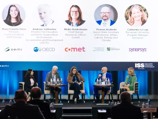
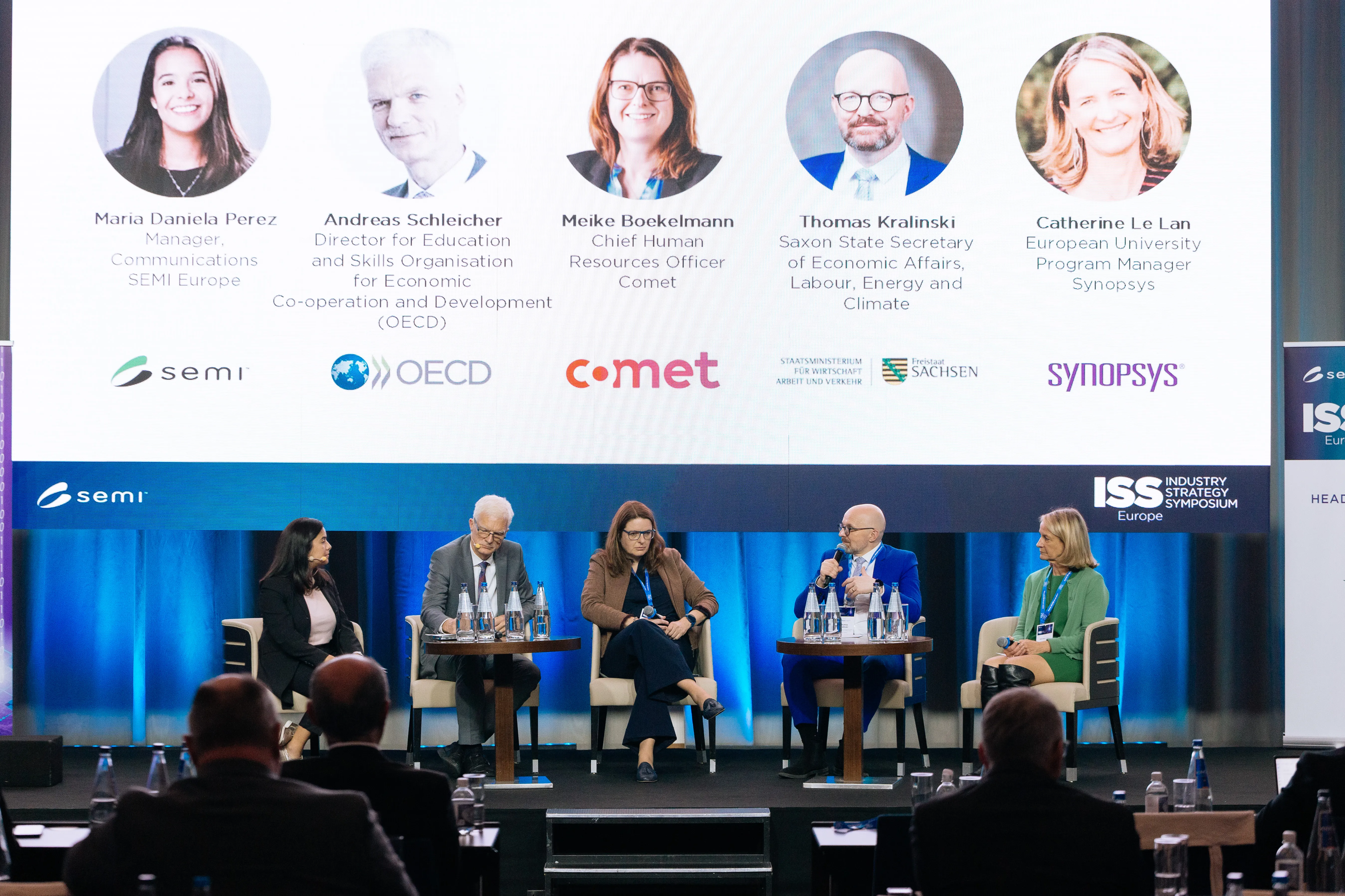
The semiconductor industry lies at the heart of Europe’s technological ambitions, powering breakthroughs in artificial intelligence, quantum computing, and advanced manufacturing. However, as the industry expands rapidly to meet surging global demand, the need for highly skilled workers is outpacing supply. According to the recently published ECSA Skills Strategy, Europe must train and hire tens of thousands of skilled professionals by 2030 to remain globally competitive. Without a robust and inclusive talent pipeline, the region’s independence in critical technologies might be at risk.At this year’s Industry Strategy Symposium Europe (ISS Europe) held in March, a panel discussion moderated by Maria Daniela Perez from SEMI Europe, brought together industry leaders and experts to explore solutions to this challenge. The discussion centered on how emerging technologies are reshaping the workforce, the role of education in preparing future professionals, and strategies for attracting and retaining diverse talent – all critical to ensuring sustainable workforce development in the semiconductor industry.Tackling Talent Acquisition and RetentionCatherine Le Lan, European University Program Manager from Synopsys, drew a direct connection between technological disruption and workforce challenges. “AI is driving unprecedented changes, and hardware is at the heart of the AI revolution,” said Le Lan. As the industry invests in new methodologies, leading-edge technologies, and innovative products, the demand for updated skillsets continues to outpace supply. This places a dual burden on companies – who must hire for both today’s and tomorrow’s skills – and on the education sector, which is expected to rapidly adapt.Meike Boekelmann, Chief of Human Resources at Comet, highlighted that the challenge is not just about attracting talent from within the semiconductor field – it is also about standing out in a crowded talent market. “We are not only competing within our industry for talent. We’re also competing against other industries: automotive, consumer electronics, and AI,” said Boekelmann. To succeed, companies must go beyond traditional incentives and offer meaningful, forward-looking career experiences. “Primarily what I see is that they’re really asking for creating an impact and also a sense of belonging… so they want to see what’s the outcome,” she explained. “There are more people leaving the labor market than entering the labor market,” added Thomas Kralinski from the Saxon State Secretary of Economic Affairs, Labour, Energy and Climate. “We need to think about immigration, family-work integration, and training.” His comments underscore the need for a holistic workforce strategy – one that not only fills immediate vacancies, but also strengthens the broader ecosystem through inclusive policies, targeted reskilling, and long-term demographic planning.Fostering Industry-Academia SynergyAs the industry evolves, so must its workforce. Andreas Schleicher, Director for Education and Skills at the OECD, made a stark observation. “There’s one thing worse than losing people – and that is to keep them and not upskill them.” He warned that the current pace of technological change demands far more than one-time training; it requires a culture of continuous learning. “Neither the industry nor the education sector has the capacity for upskilling and reskilling,” he noted, pointing out that while Europe performs well in early education, adult learning remains insufficient. “The incidence and intensity of upskilling and reskilling is so far out of what we will need.” Without scalable, lifelong learning systems, even experienced professionals risk being left behind.Building on this idea of future-readiness, Thomas Kralinski noted: “Do you know what kind of fab is going to be open in 10 years’ time or what startup is going to be founded in 10 years’ time? You probably don’t. But everybody who’s working there or will work there is born already – and is probably in school or at the university.” He underscored the need for steady investment in teachers, training systems, and educational infrastructure – not just to meet today’s demand but to ensure Europe’s long-term competitiveness.To truly inspire the next generation, Schleicher pointed to visibility as a vital factor. “You cannot be what you cannot see.” Without relatable role models or a clear understanding of how their interests connect to meaningful careers, young people – especially underrepresented students – often overlook STEM pathways. Schleicher described how even small actions, like industry professionals visiting schools to explain their work, can have a lasting impact. “You can bring someone from the semiconductors industry to speak to students and help them understand, for example, what’s in a mobile phone and that they can actually create tomorrow’s mobile phone.” That kind of engagement, he argued, helps “build dreams” and makes technology tangible, exciting, and inclusive.AI: An Enabler, Not a ThreatPanel moderator Maria Daniela Perez raised a critical question about the evolving role of AI in the workforce. Acknowledging the widespread concern that AI could lead to job displacement, she challenged the panel to consider a different perspective. How can AI be leveraged to broaden and accelerate the talent pipeline rather than replace it? In response, the panelists emphasized that AI is not a disruptor but an accelerator. Rather than eliminating jobs, AI-driven tools enhance productivity by automating repetitive tasks, freeing professionals to focus on innovation, problem-solving, and high-value work. Catherine Le Lan provided a compelling example, explaining how AI-powered electronic design automation (EDA) tools are enabling engineers to push the boundaries of technological advancement. She referred to a university study that compared two groups of students – one with access to AI tools and one without. “They found out that those AI tools helped to improve productivity and also helped to improve skills of the students,” she said. “The student who had used AI tools had better skills than the one who hadn’t used AI tools… because they had been able to focus on the high-level skills, and they got rid of the low-level skills.” Her remarks underscored how AI, when integrated into education, can accelerate both efficiency and learning outcomes.Collaboration: The Key to Sustainable Workforce DevelopmentAddressing the workforce challenge requires cross-sector collaboration among industry, academia, and policymakers. There is a shared responsibility to invest in long-term education strategies, develop structured training initiatives, and create an ecosystem where talent can thrive. This is precisely the mission of two SEMI Europe-led initiatives.The European Chips Skills Academy (ECSA) and the European Chips Diversity Alliance (ECDA) are playing a critical role in shaping Europe’s semiconductor workforce. ECSA is driving efforts to align education and training with industry needs, ensuring that both students and professionals are equipped with the technical expertise and practical experience required for the sector’s future. Meanwhile, ECDA focuses on building a more inclusive semiconductor workforce across the industry. By creating opportunities for underrepresented groups, ECDA is ensuring that the industry benefits from a broad talent pool.Securing Europe’s Semiconductor FutureIn her closing remarks, Maria Daniela Perez brought the discussion full circle, emphasizing that addressing the semiconductor talent gap requires collective ownership: “In the end, it ends up being all about collaboration,” said Perez. From engaging technology users to amplifying the industry’s visibility, to aligning with academia and policymakers, the path forward depends on shared action. By fostering this ecosystem-wide commitment – and investing in the people behind the progress – Europe can bridge the talent gap and shape a resilient, inclusive, and globally competitive semiconductor workforce.SEMI ContactKartikey Srivastava, Senior Specialist, CommunicationsEmail: [email protected]
Read More
The Rising Stars: 20 Under 30 blog series celebrates the brightest young leaders shaping the future of the semiconductor industry. These exceptional individuals have earned the SEMI Europe 20 Under 30 Award for making a remarkable impact across the supply chain—whether in engineering, sales, marketing, or R D. Nominations for the 2025 20 Under 30 Award are now open, providing the opportunity to recognize and honor the next wave of industry trailblazers.The series spotlights these rising stars for their career achievements, commitment to innovation, leadership skills, and dedication to driving both business success and community growth.Follow their inspiring journeys and discover how they are thriving and paving the way for future generations in the semiconductor world.Introducing Mariusz Grabowski: Lead Design Engineer at Cadence Design SystemsMariusz Grabowski, a 2023 20 Under 30 award recipient at the age of 24. He is now a Lead Design Engineer at Cadence Design Systems, Inc., where he’s been making strides in digital systems design for nearly three years. Prior to this role, he gained valuable experience as an FPGA Design and Verification Engineer at Aldec Inc. Grabowski holds a master’s degree with distinction in automation and robotics from AGH University of Science and Technology in Krakow, Poland. During his academic career, he was an active member of both the Avader and Integra Scientific Groups. He also achieved recognition at events like DASIP 2023 and in the International FPGA Hackathon, where he and his team earned 2nd and 3rd place. He is currently also pursuing a postgraduate degree in Project Management at SGH Warsaw School of Economics. SEMI: What inspired you to join the semiconductor industry? Grabowski: I have always been fascinated by the fundamental workings of advanced systems and that curiosity led me to pursue a career in the semiconductor industry. As a digital design engineer, it is exciting for me to contribute to the creation of such large and sophisticated architectures from basic building blocks. Now, I’m proud to be a part of Cadence Design Systems, where I can work on the cutting-edge designs with some of the most talented and hard-working engineers. Grabowski and his team at the awards ceremony at FPGA Hackathon 2023SEMI: How did your early experiences and education shape your career path?Grabowski: During my studies, I had the opportunity to work on hands-on projects with an FPGA platform, which led me to my first job as an FPGA design and verification engineer. That experience gave me a broader perspective on the industry’s scale and reinforced my passion for tackling challenges, learning and growing in this field.Grabowski presenting his paper at the DASIP 2023 ConferenceSEMI: Can you share a professional accomplishment you’re most proud of, and explain why it’s significant to you? Grabowski: For me, it is successfully balancing full-time studies with work. It was a challenging experience, but it provided invaluable opportunities to grow my skills and gain hands-on experience. During that time, I completed numerous projects, participated in scientific conferences and industry events like DASIP 2023, and even earned 2nd and 3rd place in the International FPGA Hackathon. These achievements reinforced my passion for the field and my ability to thrive under pressure. SEMI: As a young professional in the industry, what is your greatest challenge? Grabowski: One of the biggest challenges is navigating the complexity of large-scale projects, where seamless coordination between multiple teams across the globe is crucial. As someone still early in my career, gaining the experience to manage the cross-functional aspects of a project while ensuring my own contributions are technically sound has been both demanding and rewarding.Grabowski at the Discussion Panel on Industry Career Perspectives at DATE 2024 ConferenceSEMI: What advice would you give to younger generations aspiring to make an impact in this industry?Grabowski: The sheer amount of information and complexity in the industry can feel overwhelming. It is essential to embrace curiosity and continuous learning, but it is also crucial to recognize that you can’t do everything alone. My advice is to find your area of expertise and collaborate with others; teamwork is key to bringing impactful projects to life. Cadence’s Design Team in Warsaw, Poland Manager Jacek Rosiak—3rd from the leftSEMI: How do you envision future work environments? Grabowski: I envision future work environments as places where technology fosters creativity and collaboration, diversity is celebrated, and flexibility and work-life balance are prioritized. These environments will empower employees to perform at their best while feeling supported and valued. I am proud to be a part of Cadence Design Systems, where I feel that these values are strongly cultivated. SEMI: What impact has the 20 Under 30 Award had on your career? Grabowski: Receiving the 20 Under 30 Award was an incredible validation of the hard work I’ve put into my role. It gave me a confidence boost, affirming that I am on the right path and capable of making meaningful contributions to my company and the broader semiconductor industry. It also brought significant recognition, which opens up numerous opportunities.Following 20 Under 30 JourneysMariusz Grabowski’s journey in the semiconductor industry highlights the power of dedication, curiosity, and continuous learning. From his early experiences with FPGA platforms to his significant accomplishments in both academia and industry, Grabowski is a true example of how passion and hard work can drive meaningful contributions. As a young professional, his insights offer valuable inspiration for the next generation of engineers eager to make their mark in this ever-evolving field. With a bright future ahead, Grabowski is sure to continue influencing the world of technology, one innovative project at a time.The Rising Stars: 20 Under 30 blog series celebrates the exceptional talent and leadership driving the future of the semiconductor industry. Each of the young innovators honored is excelling in their respective fields while shaping the landscape of technology and business with their visionary approaches and dedication. Their stories exemplify the remarkable achievements and unwavering commitment that define the next generation of industry leaders. The series is intended to inspire and motivate future professionals to pursue their passions and embrace the opportunities within this dynamic industry. Stay tuned for more stories of rising stars who are paving the way for continued growth and innovation in the semiconductor world.Learn more about the SEMI Europe 20 Under 30 Award and the recipients honored at SEMICON Europa. SEMI ContactMaria Daniela Perez, Communications ManagerEmail: [email protected]
Read More
The Rising Stars: 20 Under 30 blog series celebrates the brightest young leaders shaping the future of the semiconductor industry. These exceptional individuals have earned the SEMI Europe 20 Under 30 Award for making a remarkable impact across the supply chain—whether in engineering, sales, marketing, or R D. The series spotlights these rising stars for their career achievements, commitment to innovation, leadership skills, and dedication to driving both business success and community growth.Follow their inspiring journeys and discover how they are thriving and paving the way for future generations in the semiconductor world.Introducing Raphael Hardegger: Product Manager Advanced Products at VATRaphael Hardegger is a Product Manager at VAT, where he leads the development of innovative atomic layer deposition (ALD) valve technology. Starting his career in 2009 as a design engineer apprentice at VAT, Raphael has since gained diverse experience, including entrepreneurial ventures and a role in MedTech. Today, he focuses on shaping product strategy, aligning solutions with customer needs, and driving impactful advancements in the semiconductor industry.SEMI: What inspired you to join the semiconductor industry? Hardegger: I joined the semiconductor industry, and VAT in particular, at the young age of 15. Back then, I started as a design engineer in VAT’s apprenticeship program. Growing up in the beautiful VAT region, my entry into the industry was somewhat by chance – but I’m incredibly glad it happened! After gaining foundational knowledge at VAT, I pursued studies in mechanical engineering, worked in various other roles and companies, and then completed a master’s in business innovation. About 3.5 years ago, the semiconductor industry pulled me back in, and I haven’t looked back since. What keeps me excited about VAT and the industry as a whole is its sheer complexity. Every day, we have the opportunity to innovate with small components that have a significant impact on a huge industry. It’s such a multifaceted field that I’m confident I’ll continue learning something new every day for the rest of my career.SEMI: How did your early experiences and education shape your career path?Hardegger: In Switzerland, the apprenticeship model uses a results-oriented work style from an early age. The lessons I learned during my four years as an apprentice at VAT continue to influence my daily work life. The mechanical foundation I built during that time remains a tremendous asset in my career. When combined with my studies in systems engineering and business innovation, this foundation has allowed me to make a meaningful impact both at VAT and within the broader industry.SEMI: Can you share a professional accomplishment you’re most proud of, and explain why it’s significant to you? Raphael Hardegger in the VAT office of San Jose, California, USA, holding the new product he worked on.Hardegger: When I rejoined VAT as a product manager, I was given the opportunity to manage a new product that wasn’t even on the market yet. This product was a key part of VAT’s strategy to outpace market growth by expanding into new product segments beyond our core offerings. I had the privilege of collaborating with some of VAT’s most talented engineers, who developed an incredible product. Together, we learned a great deal through our initial interactions with customers, refining the product to meet stringent requirements. This year, we successfully qualified the product for use in the industry’s most challenging semiconductor processes. It’s a testament to how dedication, customer-focused engineering and exceptional teamwork can make a significant impact. What makes me proud is not just working on innovative concepts, but creating products that truly excite our customers and contribute to meaningful growth for VAT.SEMI: As a young professional in the industry, what is your greatest challenge? Hardegger: I turned 30 this year, so I suspect I was one of the oldest 20 under 30 winners last year. One challenge I’ve faced — not only in this industry, but across others — is impatience. As a young professional with high aspirations, it’s easy to feel that things aren’t moving fast enough. We often expect early promotions, annual salary increases, and quick recognition for our efforts. What changed my perception on this was a conversation with a senior manager at VAT shortly after I joined. I asked him what steps I should take to move closer to my next career goal, such as earning a management position. His response was simple and direct: Focus on making an impact in your current role. Build a strong track record and demonstrate your skills. Everything else will follow. I took his advice, and I'm glad I did. No, I didn't get promoted immediately, but I learned the value of patience, doing my best every day, and finding satisfaction in the process.Career progression isn’t just about motivation and talent — it’s also about timing and aligning with the business needs. Being impatient or pushing for premature career moves can often backfire, leaving you in a worse position than before. By focusing on making a genuine impact and building a solid track record, you create a strong foundation for a fulfilling and sustainable career.SEMI: What advice would you give to younger generations aspiring to make an impact in this industry?Hardegger: You're in a great place — right where you need to be. Be curious and explore as much of the semiconductor industry as you can. During my training as a design engineer, I wasn't deeply involved in understanding the customer applications our valves were serving. My focus was primarily on developing vacuum valves based on product management requirements and manufacturing needs. Since I returned, I've learned the importance of understanding what our customers truly need and translating those needs into product requirements.This shift has not only helped me and the team create better products, but also made the work much more enjoyable! While I'd still like to deepen my understanding of customers' processes, it's already fascinating to learn more about their goals and see how our products can make a real difference. If I could go back to my apprenticeship or just starting this industry, my advice to myself — and to anyone starting out — would be to stay as curious as possible. Take every opportunity to learn what customers are trying to achieve with the products you help create. That curiosity will guide you to make a meaningful impact.SEMI: How do you envision future work environments? Hardegger: To me, having a clear customer focus in every aspect of a company's efforts is essential. At the end of the day, someone needs to want to buy our products for us to remain profitable and continue to grow. That’s why maintaining a customer-centric approach in all aspects of product development and management is critical. At the same time, the people who work in such companies need to be happy and fulfilled to create great products. I appreciate the recent trends we’re seeing to improve the corporate culture, such as embracing hybrid working models. These approaches provide a healthy balance between in-office collaboration and focused work from home, helping employees maintain productivity and well-being.SEMI: What impact has the 20 Under 30 Award had on your career? Hardegger: While I deeply appreciate the recognition that comes with such awards, I believe my career should ultimately be defined by the impact I make in my field. That said, I do hope the award inspires other young professionals to explore this exciting industry and build meaningful careers here! Following 20 Under 30 JourneysRaphael Hardegger’s journey in the semiconductor industry is a testament to the power of curiosity, dedication, and a customer-centric approach. From his early days as a design engineer apprentice to his current leadership in product innovation, Raphael continues to drive meaningful change at VAT Group. His story inspires young professionals to embrace continuous learning, focus on making a real impact, and contribute to the growth and success of the semiconductor industry.The Rising Stars: 20 Under 30 blog series celebrates the exceptional talent and leadership driving the future of the semiconductor industry. Each of the young innovators honored is excelling in their respective fields while shaping the landscape of technology and business with their visionary approaches and dedication. Their stories exemplify the remarkable achievements and unwavering commitment that define the next generation of industry leaders. The series is intended to inspire and motivate future professionals to pursue their passions and embrace the opportunities within this dynamic industry. Stay tuned for more stories of rising stars who are paving the way for continued growth and innovation in the semiconductor world.Learn more about the SEMI Europe 20 Under 30 Award and the recipients honored at SEMICON Europa. SEMI ContactMaria Daniela Perez, Communications ManagerEmail: [email protected]
Read More