downloadGroupGroupnoun_press release_995423_000000 copyGroupnoun_Feed_96767_000000Group 19noun_pictures_1817522_000000Member company iconResource item iconStore item iconGroup 19Group 19noun_Photo_2085192_000000 Copynoun_presentation_2096081_000000Group 19Group Copy 7noun_webinar_692730_000000Path
Skip to main content
Default Banner Image

semiconductor manufacturing

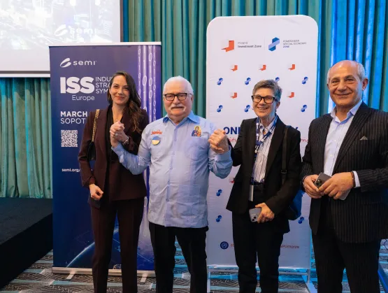
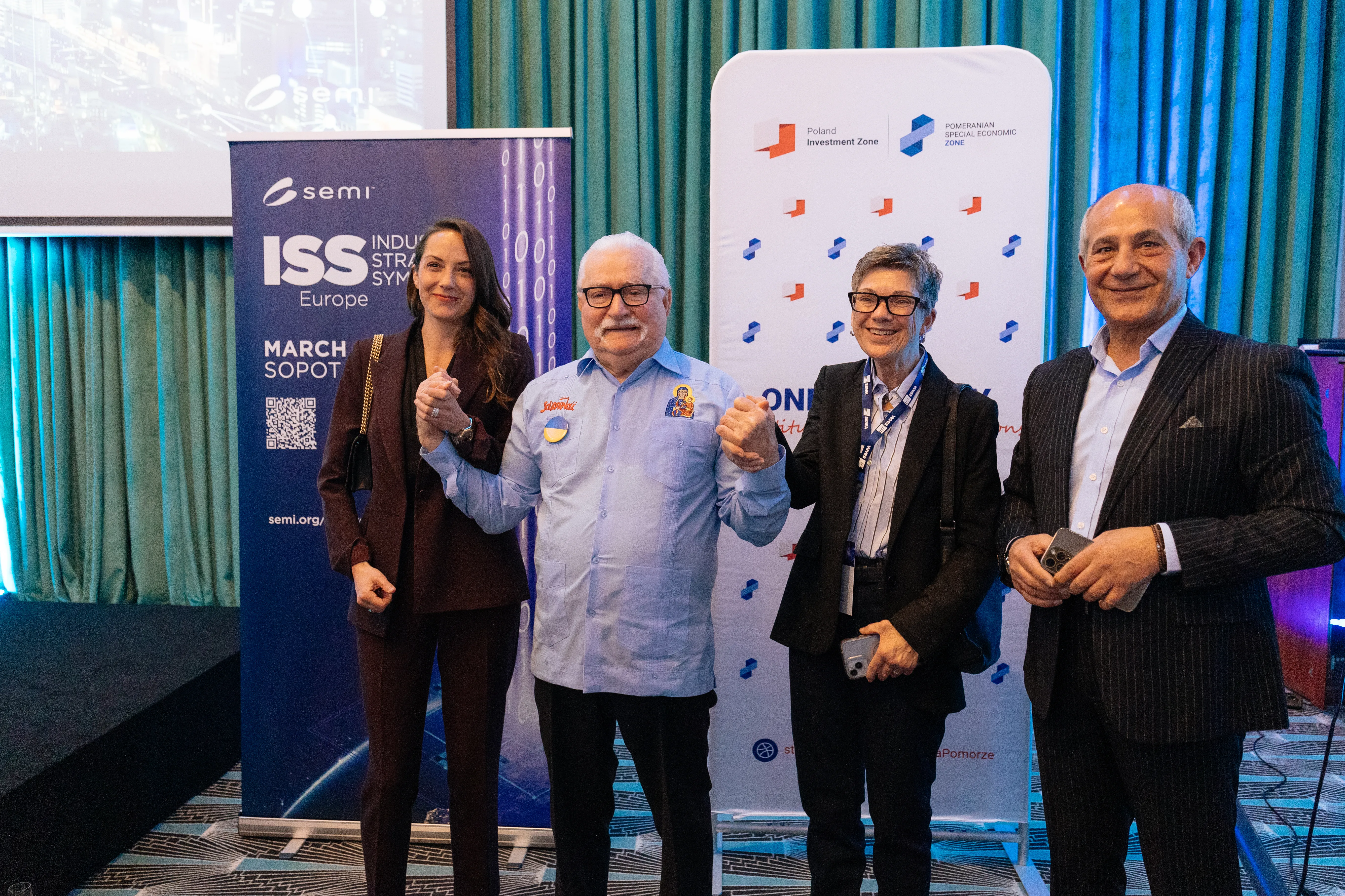
As competition within the semiconductor industry continues to intensify, the need for Europe to strengthen its current position within the global supply chain and develop new partnerships are more important than ever. How can Europe forge a unified semiconductor strategy amidst geopolitical tensions, fast‑moving technological change, and ongoing supply‑chain challenges? These dynamics set the stage for the 2026 Industry Strategy Symposium (ISS) Europe taking place in March in Sopot, Poland for the second consecutive year, bringing together leaders from across the semiconductor ecosystem to assess a rapidly shifting global landscape and define Europe’s path toward greater competitiveness and resilience.The symposium opened with a welcome speech featuring Lech Wałęsa, Nobel Peace Prize Laureate and former leader of the Solidarnosc movement which led Poland’ s resistance to its authoritarian Communist regime in the 1980s. Wałęsa shared a strong message on the importance of collaboration: “Old geopolitical structures and the bipolar world order have reached their limits, and as we transition toward a new global order, it is essential to rebuilding a system better suited to today’s realities”. In this uncertain moment, the Nobel Peace Prize called for peaceful dialogue and collective action to shape a new, more suitable world order rather than relying on conflict.Lech Wałęsa, Nobel Peace Prize LaureateAmidst geopolitical tensions, accelerating technological change, and intensifying global competition, a clear message emerged: semiconductors are now foundational to European economic security and technological leadership. As Laith Altimime, President of SEMI Europe, emphasized, “Semiconductors are the infrastructure of the modern world, and only through close collaboration can we master the challenges ahead and strengthen Europe’s technological leadership.”Laith Altimime, President, SEMI EuropeEurope plays a vital role in this industry, with global revenues expected to reach $2 trillion by 2035. As Altimime noted, “Europe has strong foundations, leading in manufacturing equipment and innovation. We must maintain this leadership while reducing dependencies.”A central theme throughout the symposium was how Europe can build on its leadership positions while strengthening its role across the value chain. As Leonard Hobbs, Director of Government Affairs at Intel Ireland, said, “No region controls the entire supply chain. Europe has to figure out how to differentiate itself within the various parts of the supply chain.” Marc Hijink, author of the book Focus – The ASML Way highlighted Europe’s deep supplier ecosystem, and explained that “more than 80% of the value in the products that ASML makes comes from suppliers who are mostly based in Europe.” Marc Hijink, Author of Focus – The ASML WayAt the same time, significant investments are reshaping Europe’s manufacturing footprint. Joerg Recklies, Executive Vice President Frontend at Infineon, drew the audience’s attention to Infineon’s upcoming Smart Power fab opening in summer 2026 “six months ahead of schedule.” Recklies added, “The new ESMC facility in Dresden is expected to produce 40,000 300mm wafers per month, and will provide the first FinFET capability in Europe.” Joerg Recklies, Executive Vice President Frontend, Infineon TechnologiesLooking at opportunities in advanced semiconductors, Cesc Guim, CEO of Open Chip, said, “25 years ago, the only way to learn how to do advanced chip design was in one of the large US companies. That’s no longer the case. Europe now has the capabilities, supported by RISC-V and a full supply chain backed by the wealth of hardware and software engineering talent in regions such as Pomerania.” Left to Right: Mikołaj Trunin, Deputy Director, Invest in Pomerania and Cesc Guim, CEO, Open ChipTo reinforce the sense of opportunity in a changing world, futurist Christian Kromme gave a whirlwind tour through the revolutions to come in technology and society. He described how each wave of technological change, from the internet to AI to autonomous machines, is arriving faster than the one before. “The internet wave commoditized media and knowledge. In the AI wave, we will see the same value compression, but this time squeezing out human skills such as problem-solving and system design,” said Kromme.Kromme urged delegates to “shift from hard skills to heart skills: imagination, empathy, curiosity and integrity, this is where the value of humans lies, because machines cannot do these things.”Christian Kromme, FuturistTrade tensions and international conflictGeopolitics and supply chain dynamics were central to the discussions. Martin Zech, Senior Director at FTI Consulting, described how the US’s approach to the semiconductor industry had shifted from incentives to restrictions. Zech warned that “a new section 301 investigation into the European semiconductor industry could lead to new tariffs.” Johan Rauer, Partner at McKinsey, added that the threat extends beyond tariffs. “Regions will apply a range of measures, including export controls and IP protection.”Martin Zech, Senior Director, FTI ConsultingJohan Rauer, Partner, McKinsey CompanyChristopher Frieling, Director of Advocacy and Public Policy at SEMI Europe, outlined the EU’s response, including its evolving economic security framework and the concept of “trusted chips,” reflecting a preference for products with strong European involvement.Christopher Frieling, Director of Advocacy and Public Policy, SEMI EuropeThe question of technological leadership was addressed by Carlos Pardo, CEO of KD, who stated, “If Europe wants a relevant position in semiconductors, it needs to invest more.” He added that even in automotive semiconductors, European players hold relatively limited shares. Carlos Pardo, CEO, KDProviding another perspective, Dr. Rafał Bugyi, CEO of TRUMPF Huettinger said, “We don’t need to cover the entire supply chain, but we must be indispensable.” Dr. Rafał Bugyi, CEO, TRUMPF Hüttinger GmbH Co. KGSpeakers also addressed how Europe could adapt to the new reality of supply chain dependency. Benoit Chassagne, End-to-End Supply Chain Manager at Edwards, presented a model of a systems response which his company has implemented to mitigate its exposure to supply chain volatility, while David Forrest, Director of Sustainability and Criticality at Vital Materials, emphasized the role of waste materials recovery, saying that “circularity is an industrial mechanism for supply chain resilience, not an environmental add-on.”Benoit Chassagne, End-to-End Supply Chain Manager, EdwardsDavid Forrest, Director of Sustainability and Criticality, Vital MaterialsCarl van Vugt Luning, Chief Commercial Officer at Resilicon, highlighted the need for greater resilience in polysilicon supply, noting Europe lacks dual sourcing. “Polysilicon is often seen as a commodity, but it is critical. Sovereign chips require a resilient polysilicon supply chain,” said van Vugt Luning.Carl van Vugt Luning, Chief Commercial Officer, ResiliconTurning innovation into commercial revenueIn the session ‘From lab to fab’, speakers examined how Europe can improve its track record in converting innovation into commercial success, for example, by companies such as NVIDIA and Qualcomm.An important part of the EU’s strategy was the creation of technology pilot lines. Jari Kinaret, Executive Director of the Chips Joint Undertaking (Chips JU), told the symposium that the pilot lines are an example of successful collaboration between the state and the private sector. Kinaret said, “The total cost of the NanoIC pilot line (for advanced semiconductor fabrication) is €2.5 billion, but this includes €1 billion of funding from ASML.”Jari Kinaret, Executive Director, Chips Joint Undertaking (Chips JU)The role and value of the pilot lines was the subject of a panel discussion at the symposium. Panelist Anne Van den Bosch, Vice President of Public R D Policies and Programs at imec, said the pilot lines “give the European semiconductor ecosystem faster access to advanced process technology.” Patrick Bressler, Director of Fraunhofer Mikroelektronik, agreed. “Pilot lines are a lab-to-industry scheme to give access to prototype manufacturing for SMEs, start-ups and fabless companies which would not otherwise be able to afford advanced manufacturing,” he said.Moderating the discussion, Laith Altimime asked, “How do we ensure that the products which emerge from innovations developed thanks to the pilot lines get manufactured in Europe? Are boutique fabs the answer?” Kevin Williams, Deputy Director of the PIXEurope pilot line, responded: “There are certainly opportunities in building new types of chips and new types of fabs. We have the know-how in the pilot lines, and the equipment for them is made in Europe.” Bruno Paing, Vice President Europe at CEA-Léti, added, “We need to aim for indispensability, replicating what we have with ASML in the EUV field. For instance, the world needs better memories and better interconnects. There are many opportunities in AI. It is not just about the GPU.”Left to Right: Moderator, Laith Altimime, President, SEMI Europe; Panelists: Anne Van den Bosch, Vice President of Public R D Policies and Programs, imec; Bruno Paing, Vice President Europe, CEA-Léti; Patrick Bressler, Director, Fraunhofer Mikroelektronik; Kevin Williams, Deputy Director, PIXEurope.The symposium also highlighted examples of European innovation from two startups developing new technologies. Antonio Mesquida Küsters, Strategic Advisor to Euclyd, presented a processor system combining 16,384 cores with ultra-high bandwidth memory using advanced 2.5D and 3D packaging, offering an alternative to GPUs for AI inference. As he said, “We want to break the hyperscaler/cloud model of AI to build sovereign AI capability for Europe by 2030.”Antonio Mesquida Küsters, Strategic Advisor, EuclydJekaterina Viktorova, Founder and CEO of Syenta, introduced additive manufacturing technology enabling denser interconnects for advanced AI systems, noting, “Our roadmap is set to produce a 20x increase in bandwidth over the next 10 years.”Jekaterina Viktorova, Founder and CEO, SyentaNew strategies for competitiveness in semiconductor manufacturingIf these types of innovative products are to be manufactured in Europe, the region’s fab operations will need to combat the growing competition from China and elsewhere. Giovanni Notarnicola, Partner at Porsche Consulting, said, “Our position in Europe is under attack. The next threat is not from a new product, but from how chips are designed and produced.”Giovanni Notarnicola, Partner, Porsche ConsultingThomas Altenmüller, Vice President of Manufacturing Analytics at Infineon, highlighted the role of automation: “We get more automation in the transition from 8” to 12” wafers, which gives us an advantage in Europe because of our higher labor cost compared to China. But to compete, we still need more AI smart workflows to increase the automation.” Carina Lainer, Principal at Roland Berger, added, “Today we optimize operations with tools built for a human-centric process, which has reached its limit. We can instead use digitalization and AI to fundamentally change the way that semiconductor innovation takes place.”Thomas Altenmüller, Vice President of Manufacturing Analytics, InfineonLeft to Right: Carina Lainer, Principal, and Thomas Kirschstein, Partner, Roland BergerOded Tal, CEO of MAX Group, cautioned that the barrier to increased implementation of automation was not technical but social. “Humans can be very flexible, but leadership is crucial. “You have to give training and clear instructions. It’s about structure, making people’s roles and responsibilities crystal-clear,” he said.Oded Tal, CEO, MAX GroupThe symposium closed with a panel discussion about the implementation of AI and automation in the fab. Moderator Cassandra Melvin, Senior Director of Business Development and Operations at SEMI Europe, pointed out that “intelligence is moving beyond the tool to the control room, a development which is powered by AI.” The panelists were quick to acknowledge the radical impact that AI is having on fab operations. Dirk Drescher, Plant Manager at Bosch Semiconductor, said, “We built the Bosch fab in Dresden around a standardized data architecture, which is what enables us to implement AI. That is a contrast to a 20 year old fab, which can only see a patchwork of different data systems.”Thomas Richter, Senior Vice President and Managing Director at Infineon, added, “digitalization is about much more than just AI. We have had great success in getting rid of boring, routine tasks through digitalization. This makes a huge difference, and helps our fabs to stay competitive.”The panel also debated the potential impact of humanoid robots on the scale and impact of automation. Richter said, “In our fabs, I can see rooms in which it has never been possible to automate before, but humanoid robots give me hope that we can automate more in future.”Matthias Bonkass, Vice President of Advanced Manufacturing Engineering at GlobalFoundries, agreed. “By 2035, we will see collaboration between humans and humanoids. This wave is coming!” Going even further, Dirk Drescher looked forward to an era of total automation. He said, “We will see a lights-out fab by 2035. This is definitely a tailwind for the European semiconductor industry, making it faster, reducing cost, and giving us more opportunity to build semiconductors in Europe.”Thomas Morgenstern, Executive Vice President of Manufacturing at STMicroelectronics, concluded, “We must not let culture be a barrier to AI. Technical strategies to implement AI are all very well, but you need people to buy in. Morgenstern added, “The name of the game is productivity. The most advanced fabs have to be dark, with remote operating centers somewhere in the world, running clusters of fabs. I am extremely confident that by 2035, if not before, the first dark fab will be in operation.”Left to Right: Moderator, Cassandra Melvin, Senior Director of Business Development and Operations, SEMI Europe; Panelists, Dirk Drescher, Plant Manager, Bosch Semiconductor; Matthias Bonkass, Vice President of Advanced Manufacturing Engineering, GlobalFoundries; Thomas Morgenstern, Executive Vice President of Manufacturing, STMicroelectronics; Thomas Richter, Senior Vice President and Managing Director, Infineon.During the event, SEMI Europe announced recipients of the SEMI European Award and Special Service Award for 2025. Dr Peter O’Brien, Head of Research in Photonics Packaging and Systems Integration at Tyndall National Institute, was honored with the SEMI European Award and, Eric Beyne, Senior Fellow at imec, with the Special Service Award. Peter O’Brien, Head of Research in Photonics Packaging and Systems Integration, Tyndall National InstituteAnne Van den Bosch, Vice President Public R D Policies and Programs, imec receiving the award on behalf of Eric Beyne, Senior Fellow, imecOn behalf of SEMI, the SEMI Europe team and ISS Europe committee, we would like to thank all speakers, sponsors, and attendees for making the event a great success. ISS Europe 2027 will take place in Dresden, Germany from March 8-10.Serena Brischetto is Director, Marketing and Digital Engagement at SEMI Europe.
Read More
The CxO Summit at SEMICON Europa 2025 spotlighted Europe’s ongoing efforts to build a resilient and globally competitive semiconductor industry, while calling for greater ambition, speed, and unity in execution. Following global disruptions with the automotive supply chain crisis, the European Union launched a continent-wide strategy through the EU Chips Act. While the Act has already spurred significant developments, including construction of the new ESMC fab in Dresden, Europe remains far from its goal of achieving a 20% share of global semiconductor production by 2030. The CxO Summit, part of the SEMICON Europa event in Munich, provided an opportunity for industry leaders to share ideas about how to catalyze the next phase of the European industry’s growth.Ajit Manocha, President and CEO of SEMI opened the summit by describing today’s industry landscape with one word: “unprecedented.” Manocha said, “The global growth of the industry is unprecedented, with 107 new fabs set to come online by 2028, but the uncertainties are unprecedented, from geopolitics to the talent shortage to environmental concerns. So we need unprecedented solutions.” Ajit Manocha, President and CEO, SEMILaith Altimime, President of SEMI Europe echoed the mood of uncertainty, describing Europe as caught “in a perfect storm.” Altimime said, “As we face a combination of internal challenges and intensifying external competition, collaboration is not optional — it is mission critical.” Laith Altimime, President, SEMI EuropePierre Chastenet, Head of the Unit for Microelectronics and Photonics, European Commission, highlighted the tangible progress made under the EU Chips Act. “We now have a proper toolbox to handle a future crisis in the supply chain. The Chips for Europe initiative has led to the creation of five pilot lines for advanced technologies such as FD-SOI and wide bandgap semiconductors.” Chastenet added, “Europe must now capitalize on its strengths, from materials and equipment to design tools and cutting-edge research emerging from our RTOs.”Pierre Chastanet, Head of the Unit for Microelectronics and Photonics, European CommissionEchoing the call for action, Oliver Schenk, Member of the European Parliament, urged stronger regional unity. “Europe must act together, act faster, and act with much bigger ambition,” Schenk said, reinforcing the need for cross-border commitment to strengthen the continent’s semiconductor position.Oliver Schenk, Member of the European Parliament, European ParliamentHighlighting Europe’s most critical technology gap, Luc Van den hove, President and CEO of imec, unveiled plans for a new advanced fab backed by €2.5 billion in investment from the EU, the Flemish government, and ASML. Van den hove urged Europe to commit wholeheartedly to advanced technologies: “We must be more ambitious, and focus on disruptive breakthroughs rather than incremental change if we want to ensure a prosperous future.”Luc Van den hove, President CEO, imecAt the CxO Summit, CEA-Leti and ASML signed a memorandum of understanding (MoU) to deepen their collaboration and accelerate innovation in mainstream semiconductor technologies. Building on promising results in hybrid bonding, the partnership will now target 'More-than-Moore' innovations, including heterogeneous integration and novel substrates like SiC and GaN. “We aim to combine ASML’s world-class lithography expertise with CEA-Leti’s system-level innovation,” said Sébastien Dauvé, CEO of CEA-Leti. The collaboration is set to strengthen Europe’s ecosystem by shortening the path from early research to industrial impact.Left: Anne Hidma, Senior Vice President EUR US, ASML; Right: Sébastien Dauvé, CEO, CEA-LetiTurning to Europe’s industrial base, Christian Senger, CEO of Volkswagen Autonomous Mobility, emphasized the need to shift from risk-aversion to opportunity. While the region’s automotive sector faces intense global competition, particularly from China, Senger highlighted that Europe has the potential to lead in new mobility markets. “The market for autonomous roboshuttles for people transport in large cities is forecast to be worth €400 billion in the US and Europe alone,” he said. With American firms like Waymo and Uber leading the robotaxi space, Senger stressed that Europe must “act swiftly to create an environment that supports an autonomous mobility industry here.”Christian Senger, Member of the Board for Fully Autonomous Mobility and Transport CEO of ADMT GmbH, VolkswagenEurope’s Potential to Create Advanced TechnologyOne of these RTOs, CEA-Leti, is responsible for the FAMES pilot line for FD-SOI technology. Sébastien Dauvé, CEO of CEA-Leti, agreed with Pierre Chastenet that the pilot lines show great promise. He said, “FD-SOI is a big trend in semiconductors, because it enables very low power consumption in embedded devices. We think that adoption of the technology will grow in the coming years, and that is good, because most of the technology is produced in Europe.”Sébastien Dauvé, CEO, CEA-LetiEurope is also widely recognized to be the leading global voice on sustainability – a huge issue of concern to the semiconductor industry. Henri Berthe, President of the Semiconductor and Battery Segment at Scheider Electric, told the summit that 500 million tonnes of CO2 emissions per year are attributable to the semiconductor industry – “more than the whole of Mexico emits!” he said. “We need to make fabs more efficient, and that is why Schneider Electric has launched a new playbook with Applied Materials for sustainable energy abundance for the industry.”Henri Berthe, President of the Semiconductor Segment, Schneider ElectricAnother aspect of Europe’s playbook is support for new fabs. The flagship is ESMC, the joint venture between TSMC, NXP Semiconductors, Bosch, and Infineon. Christian Koitzsch, president and managing director of ESMC, reported to the summit that the project to build in Dresden a 12nm FinFET foundry and a 28nm CMOS line, requiring a total investment of €10bn, is on schedule. “We are now developing local supply chains, hosting a series of ESMC Supplier Days which are open not only to German but generally to European suppliers,” said Koitzsch.Christian Koitzsch, President and Managing Director, European Semiconductor Manufacturing Company (ESMC)As Manfred Horstmann, General Manager and Senior Vice President of Global Foundries, pointed out, the building of the ESMC fab means that Dresden is established as the center of a cluster of semiconductor industry companies. “Global Foundries has its Fab 1 and a mask center in Dresden. In fact, one-third of the chips produced throughout the whole of Europe now comes from Dresden.”Manfred Horstmann, General Manager and Senior Vice President, GlobalFoundriesAn example of ambition was given by Terence Gan, Executive Director of the Institute of Microelectronics of Singapore. Gan told the summit how Singapore has used pilot lines to stimulate research and development in new technologies. He said: “We started research into advanced packaging as long ago as 2011. Most people thought we were mad! But today, there is strong demand for our advanced packaging capabilities because of the rise of AI and its need for high-performance computing.”Terence Gan, Executive Director, Institute of MicroelectronicsBreaking Barriers to ProgressDespite momentum, bureaucratic inefficiencies continue to hamper progress. Narjiss Haddaoui, Managing Director of European Economics called for faster decision-making: “In global competition, speed is a decisive factor. To act fast enough, the EU must change its ‘software’ - the processes by which it considers and makes decisions.” Narjiss Haddaoui, Managing Director, European economicsThe stifling character of European bureaucracy is reflected in the region’s approach to building fabs. Herbert Blaschitz, Executive Vice President of Advanced Technology Facilities at Exyte, compared fab construction timelines: 20 months in Taiwan, 34 in Europe, and 38 in the U.S., attributing delays in Europe to paperwork bottlenecks.Herbert Blaschitz, Executive VP of Advanced Technology Facilities, ExyteFabio Gualandris, President for Quality, Manufacturing and Technology at STMicroelectronics raised another concern — 100% of raw materials used in European fabs come from outside the region. Christophe Frey, Vice-President for EU Engagements at Arm France, added that geopolitical tensions are clouding the path forward: “We are a bit lost in the smoke from the big fire in the world’s semiconductor industry.” Fabio Gualandris, President Quality, Manufacturing Technology, STMicroelectronics Christophe Frey, Vice-President of EU Engagements, Arm FrancePlaybooks For Future SuccessSo amid the uncertainty and global tension, what lessons can the industry learn from successful regional examples? Tuomas Korpela, Business Development Senior Manager at Nokia, credited Finland’s strategic procurement and policy tools with enabling a vibrant semiconductor ecosystem: “Finland creates demand for advanced chips using industrial policy tools, alongside strategic procurement in sectors such as defense and aerospace, and connectivity.” Tuomas Korpela, Business Development Senior Manager - Corporate Development Organization, NokiaAt a regional level, Joerg Schulze, Director of the Bavarian Chips Alliance, said that his organization was supported by the Bavarian State Ministry of Economic Affairs, as well as by companies and universities. “We help semiconductor companies to establish themselves and grow here through help with site searches, networking and contacts, funding and support, and talent acquisition,” said Schulze.Joerg Schulze, Spokesperson for the Bavarian Chips Alliance, Director of the Fraunhofer IISB, Bayern Innovativ GmbHCompanies in the European semiconductor supply chain also provided the summit with their insights into the roots of global success. André Grede, Chief Technology Officer of Comet, described how his company’s strategy is not to wait for customers to tell it what they need, but to be “ahead of the curve.” Grede said: “Is staying in sync with the customer enough? Not for us - we are deeply embedded with our customers, and constantly looking to broaden our relevance to them.”André Grede, CTO, CometChristophe Maleville, Chief Technology Officer of Soitec, provided a real-world example of how this is done. He said: “Our engineered substrates using RF-SOI technology reduce the drain on a mobile phone’s battery power, and cut our customers’ board footprint thanks to RF front end integration. As a result, our products are now in 100% of 5G smartphones.”Christophe Maleville, CTO, SoitecAnne Hidma, Senior Vice-President for Europe and the US at ASML, shared the company’s success formula: “The reasons for ASML’s success include customer focus – decide which markets you are going to be in, and which you are not. We are also all-in on innovation. We nurture an ecosystem, which for us includes imec and CEA-Leti, as well as partnerships with academia. And lastly, we have a strong supply base, which is a core strength of Europe.” In a time marked by both uncertainty and opportunity, the example of ASML shows how the European semiconductor supply chain can survive and thrive.Anne Hidma, Senior Vice President EUR US, ASMLEurope’s Path ForwardThe CxO Summit made one thing clear: Europe has world-class innovation, policy momentum, and industrial commitment. What’s needed now is faster execution, deeper collaboration, and the courage to invest in the technologies of tomorrow. As the industry heads toward the $1 trillion milestone, the decisions made today will shape Europe’s place in the semiconductor world for decades to come.On behalf of SEMI, the SEMI Europe team would like to express appreciation to the industry leaders for sharing their visions and readiness to collaborate during the CxO Summit.SEMI ContactLaith Altimime, President SEMI [email protected]
Read More
Silicon carbide (SiC) has become a cornerstone of next-generation power electronics, driving advancements in electric vehicles, renewable energy, and industrial applications. After several years of rapid capacity expansion, the SiC industry is now entering a new phase focused on optimization, quality, and long-term scalability.This transition reflects a broader realignment across the global semiconductor ecosystem. As new fabs come online and supply chains mature, the industry is prioritizing stability, cost efficiency, and technical excellence over sheer capacity growth. SiC has moved from being a niche technology to a critical enabler of the energy transition, and this maturity demands not only investment in tools and materials, but also in process knowledge, cross-industry standards, and long-term partnerships that can sustain innovation at scale.To understand how this shift is unfolding, SEMI Europe spoke with Dr. Mark Puttock, Senior Director, Technology and Innovation at Entegris. Puttock shared his perspective on the industry’s evolution and how strategic collaboration and process innovation are shaping the next chapter of SiC manufacturing.From Ramp-Up to RefinementThe early growth of SiC manufacturing was driven by surging demand for high-efficiency power devices, particularly in electric vehicles. According to Puttock, that expansion period has given way to a new focus on yield, uniformity, and process control.The industry is entering a stage of maturity where success depends on optimization rather than scale alone. Improving consistency across crystal growth, wafer, and device fabrication is becoming just as important as adding capacity. This refinement phase calls for closer integration between materials science and manufacturing technology to ensure reliability and cost efficiency.A Focus on Process and Materials InnovationAs SiC moves toward high-volume production, challenges related to contamination control, defectivity, and wafer uniformity are taking center stage. Puttock noted that addressing these issues requires collaboration between materials suppliers, equipment manufacturers, and device makers.Efforts across the industry are converging on similar goals: enhancing purity, improving process repeatability, and developing new methods to enable larger wafer formats. Moving from 6-inch to 8-inch SiC wafers, for example, is widely recognized as a key step toward higher throughput and cost efficiency. Puttock emphasized that innovation in materials science and manufacturing technology must go hand in hand to support this scaling trend.Insights from Cross-Industry CollaborationA recent Entegris blog post featuring insights from Volkswagen Group Components and Porsche Consulting explores how SiC adoption is reshaping manufacturing strategies beyond the semiconductor industry. The post also highlights the strategy paper developed by Porsche Consulting in collaboration with Entegris. This joint effort demonstrates the value of aligning semiconductor-grade precision with automotive manufacturing demands. By sharing perspectives across industries, partners can accelerate best-practice adoption and strengthen the overall ecosystem for wide-bandgap technologies.Building a Sustainable FutureSustainability remains an integral part of this optimization phase. SiC devices themselves enable energy efficiency in end applications, but the way they are manufactured is equally important. Optimizing material use, recycling process consumables, and improving chemical delivery efficiency all contribute to a smaller environmental footprint. As production scales, attention to both performance and sustainability will be key to long-term success.Looking ForwardThe transition from expansion to optimization marks a pivotal moment for SiC manufacturing. Industry focus is shifting from building capacity to mastering control, quality, and resource efficiency. Puttock sees the future of SiC as one shaped by deeper digital integration, data-driven process development, and continued collaboration across disciplines. These advancements will help enable more consistent, sustainable, and cost-effective production—laying the foundation for the next generation of high-performance power devices.At the same time, Entegris continues to invest in materials science, contamination control, and advanced process technologies that help its customers overcome the complex challenges of SiC manufacturing. By combining technical expertise with a collaborative approach, the company plays an active role in supporting the industry’s transition toward more efficient and sustainable production.James Lam is Business Development Manager at SEMI Europe.
Read More
New pilot lines offer European innovators access to the most advanced semiconductor technologies for product development and validation.The global semiconductor landscape has undergone significant transformation in recent years. With disruptions such as the semiconductor supply chain crisis and the challenges it posed to the automotive sector, Europe’s dependence on external fabrication facilities, particularly in Taiwan, has become a pressing concern. In response, the European Union (EU) introduced the EU Chips Act, a comprehensive framework designed to reduce this reliance and boost Europe’s share of the global semiconductor market. ITF Chip into the Future, hosted by imec at SEMICON Europa 2024, was a pivotal event that brought together industry leaders, policymakers, and experts to explore the implementation of the EU Chips Act and the future of Europe’s semiconductor ecosystem. Jari Kinaret, Executive Director of the Chips Joint Undertaking (Chips JU)—the body overseeing the EU’s semiconductor investments—explained, “The Chips JU is about capacity building to drive semiconductor innovation in Europe. We will continue to be dependent on the rest of the world, but we want to make sure that the rest of the world depends on us as well.” Jari Kinaret, Executive Director, Chips JUEuropean research is driving progress towards sub-nanometer fabricationOne of the pilot lines, located at imec’s research center in Belgium, is focused on advancing methods that push Moore’s Law forward by achieving smaller and more efficient circuit features. As Luc Van den hove, President and CEO of imec, explained, “imec is now powering innovation for tomorrow’s chip designs, including stacked layers of chips, with each layer containing specific functionality implemented on chip processes optimized for each function. This allows us to scale much further than if all functionality had to be implemented on a single monolithic layer.”Luc Van den hove, President and CEO, imec Another pilot line, based in France and operated by CEA-Leti, is focused on pushing the limits of technology across multiple dimensions. CEA-Leti CEO, Sébastien Dauvé, explained that the goal of the FAMES pilot line is to advance “not only FD-SOI at 10nm and 7nm nodes, but also novel non-volatile memory technologies, RF components, 3D integration, and the development of small inductors for DC-DC converters.” Sébastien Dauvé, CEO, CEA-LetiAdvancements in 3D integration and chiplet technologies are closely tied to innovation in chip packaging. Christoph Kutter, Executive Director of Fraunhofer EMS, described how the Advanced Packaging and Heterogeneous Integration for Electronic Components and Systems (APECS) pilot line in Germany is designed to meet the needs of industrial customers’ growing demand for advanced packaging solutions. Kutter noted “Customers told us that they needed to integrate logic and power, sensors and logic, and other combinations of functions. We have built the APECS pilot line to provide what they asked for.”Christoph Kutter, Executive Director, Fraunhofer EMSThe EU Chips Act is spurring investments not only in chip fabrication but also in the underlying technologies which support chipmaking. Emmanuel Sabonnadière, EVP at Soitec, highlighted how fabrication of advanced silicon carbide (SiC) power devices “is enabled by SmartSiC™ technology from Soitec – part of a built-in-Europe solution for silicon carbide.” Sabonnadière explained that SmartSiC technology “creates very thin layers of SiC material which make really differentiated substrates supporting the production of high-performance SiC devices.” Emmanuel Sabonnadière, EVP, SoitecInnovation in materials emerged as an important theme at ITF Chip into the Future. Julien Arcamone, Vice President of Corporate R D at ASM, described the critical role of materials for atomic layer deposition (ALD) in the advancing 3D semiconductor integration. Arcamone emphasized the importance of collaboration across the semiconductor value chain, describing ASM’s partnership with imec as part of “a win-win ecosystem.” Julien Arcamone, Vice President of Corporate R D, ASMDeveloping the skills to implement advanced semiconductor technologiesWhile the EU Chips Act is subsidizing the construction of new facilities including pilot lines needed for the hardware of the semiconductor industry’s expansion – the ITF speakers underlined the equally important “software” element of the semiconductor industry ecosystem: the knowledge and expertise of the people working in the industry. One of the biggest challenges in implementing the EU Chips Act is addressing Europe’s talent gap. Katrien Marent, Executive Vice President and Chief Marketing and Communications Officer at imec, said that the gap is in part “because students who graduate in STEM subjects are not trained in advanced semiconductor technologies.” From left to right: Katrien Marent, Executive Vice President and Chief Marketing and Communications Officer, imec; Julien Arcamone, Vice President of Corporate R D, ASM; Thomas Heurung, CEO, Siemens EDA; Frédérique Le Grevès, President STMicroelectronics France and Executive Vice President, Europe France Public Affairs, STMicroelectronics; Romano Hoofman, Director imec.IC-link, imec; and Christophe Frey, Vice-President of EU engagements Managing Director, ARM.Thomas Heurung, CEO of Siemens EDA, highlighted the need for educational reform in the electronics industry. He suggested that “we might not have the right degree-level curriculum for changing times in the electronics industry. We need to change the way that we train students at university, and we need more scope for early or mid-career training on specialist micro-curriculums aimed at a particular skill or knowledge set.”The industry also struggles to attract individuals. Frédérique Le Grevès, President of STMicroelectronics France and Executive Vice President, Europe France Public Affairs of STMicroelectronics, emphasizes the importance of rebranding the industry to attract new talent. She remarked, “The word ‘semiconductor’ itself isn't very exciting—it’s even off-putting to some. By simply changing the name of educational programs, we’ve seen significant increases in enrollment. This demonstrates the power of language in shaping perceptions and interest.”Thomas Heurung of Siemens EDA also called for a stronger emphasis on entrepreneurship, noting “there is a big contrast between Europe and the US, particularly Silicon Valley.” He explained how his company’s Cre8Ventures unit had been set up to help start-ups through the key stages of creating a successful new company, including product development, attracting funding, and bringing the product to market. Thomas Fleischmann, Program Manager at Robert Bosch, explained how the EU Chips Act has accelerated the formation of the European Semiconductor Manufacturing Company (ESMC) joint venture, in which Bosch is a key stakeholder. ESMC is building a new semiconductor fabrication plant in Dresden, dedicated to producing chips for the automotive and industrial sectors. Fleischmann emphasized that ESMC will play a crucial role in helping Europe “scale advanced technologies to high volumes at a competitive cost.”In addition, the EU Chips Act also provides a broader platform for the expansion of Europe’s deep tech capacity. This includes the creation of five pilot lines, which will offer European companies access to manufacturing capacity for prototyping at the most advanced semiconductor technology nodes.Thomas Fleischmann, Program Manager, Robert BoschITF Chip into the Future at SEMICON Europa 2024 highlighted the broad scope of the EU Chips Act – not only supporting the building of advanced fabs but also providing the foundations for technology development, production, and marketing – all aimed at supporting semiconductor innovation in Europe. SEMI ContactMaria Daniela Perez, Communications ManagerEmail: [email protected]
Read More
Leaders in the semiconductor industry are finding ways to balance rapid demand growth with strategies to mitigate the risks of geopolitical uncertainty and a complex supply chain.At the CxO Summit during SEMICON Europa, industry leaders gathered to share insights into the immense opportunities ahead for the semiconductor sector, as well as the challenges that could impede growth. Laith Altimime, President of SEMI Europe, highlighted how discussions last year centered on reaching $1 trillion in global sales by 2030. “The conversation today is about how far above $1 trillion we will be in 2030,” said Altimime. “Artificial intelligence is an amazing and exciting technology, and the semiconductor industry is at the heart of it.”Laith Altimime, President, SEMI EuropeAjit Manocha, President and CEO of SEMI, described the current state of the semiconductor industry with one word – “unprecedented”. Emphasizing quantum computing as the next growth driver after AI, Manocha urged leaders to prepare for the next landmark - $4 trillion in global sales by 2040. However, the challenges facing the industry are equally unprecedented. Manocha identified four key obstacles: geopolitical volatility, the Net Zero challenge, the competition for top talent, and supply chain disruptions. “We need to work together to solve these challenges – we need unprecedented collaboration,” he explained. Ajit Manocha, President and CEO, SEMIA European Perspective on the Industry’s ChallengesWith the CHIPS Act in the US and the European Union (EU) Chips Act, the industry is also seeing unprecedented governmental engagement. Gustav Kolbe, Acting Director of Enabling and Emerging Technologies at Directorate-General for Communications Networks, Content and Technology of the European Commission, explained that Europe had been deeply impacted by the effect of trade tensions and supply chain disruptions. “In the field of semiconductors, we realized that we cannot keep doing business as usual and expect to achieve more resilience and reduced dependence on non-European supply chains,” Kolbe said. Gustav Kolbe, Acting Director of Enabling and Emerging Technologies, DG CONNECT, European CommissionJari Kinaret, Executive Director of the Chips Joint Undertaking (Chips JU), which is responsible for implementing EU Chips Act programs, described how its projects amplify the effect of EU funding by leveraging matching contributions from member states and participating companies. “This means that our budget of €4 billion actually produces investments in the semiconductor industry of about €11 billion,” he noted. Jari Kinaret, Executive Director, Chips JUThe Chips JU funded projects are designed to position Europe at the forefront of advanced semiconductor technology. Belgium’s imec, for example, is operating a Chips JU pilot line focused on leading-edge semiconductor innovation. Luc Van den hove, President and CEO of imec, highlighted the potential for 3D integration, “We can now combine multiple chips through silicon interposers with very fast connectivity between them. This allows us to build compute platforms which are far larger than what can be made with a single silicon chip,” he explained referring to this approach as “CMOS 2.0.” However, Van den hove warned that Europe cannot achieve its goals alone, emphasizing the complex semiconductor value chain and the need for collaboration. “Self-sufficiency leads to mediocrity,” he warned, advocating for a global approach that leverages the “best of the best.”Luc Van den hove, President and CEO, imecStephan Haferl, Chief Executive Officer of Comet Group, introduced the CA20, a tool designed to improve efficiency and quality in semiconductor manufacturing. The CA20 uses advanced imaging and AI to quickly identify and address production challenges, such as defects in solder bumps, without damaging components. Now fully automated, it integrates smoothly into factory workflows, providing real-time information to help manufacturers maintain high standards and increase production yields. This innovation highlights the role of new technologies in overcoming key obstacles and driving progress in the semiconductor industry.Left to right: Isabella Drolz, Vice President Marketing Product Strategy, Comet Yxlon; Laith Altimime, President, SEMI Europe; Stephan Haferl, Chief Executive Officer, Comet Group; and Dionys van de Ven, President, Comet YxlonCarlos Mazure, Chief Strategy Officer at Institute of Microelectronics – A*STAR in Singapore, illustrated this point by highlighting the institute’s focus on advanced packaging, a key Singaporean strength. “We have built a state-of-the-art 300mm prototyping line, enabling companies to implement wafer-to-wafer and chip-to-wafer bonding as well as fanout chip packaging,” Mazure said. Carlos Mazure, Chief Strategy Officer, Institute of Microelectronics – A*STARTurning back to Europe, Pierre Barnabé, CEO of Soitec, highlighted materials science as a regional strength. Soitec’s engineered substrates are driving energy efficiency breakthroughs in electronic, acoustic, and photonic applications. “We can bond anything to anything, creating advanced substrates for any active layer,” Barnabé explained. Pierre Barnabé, CEO, SoitecKai Beckmann, Member of the Executive Board and CEO Electronics at Merck KGaA, Darmstadt, Germany, also emphasized the role of materials in enabling sustainable growth. “The semiconductor industry faces a challenge with the contribution of process gases to its total greenhouse gas emissions. We hope to solve the problem by using AI to support materials research, and to design new molecules – an approach we have learned from the pharmaceuticals industry,” Beckmann shared. Kai Beckmann, Member of the Executive Board and CEO Electronics, Merck KGaA, Darmstadt, GermanyCollaboration Strengthens the Semiconductor Supply Chain Despite the breadth of enabling technologies emerging from Europe, the rapid growth in semiconductor demand has not always been matched by a secure supply. Barbara Frenkel, Member of the Executive Board Purchase at Porsche, shared that the company is collaborating with the industry to improve its access to the chips needed for automotive electrification. This includes joining industry groups such as the SEMI Global Automotive Advisory Council (GAAC) and, as she said, “learning your language.” Frenkel added, “Porsche aims to emulate Apple’s approach with Intel and Motorola to drive innovation – we will do the same with suppliers of automotive chips.”Barbara Frenkel, Member of the Executive Board Purchase, PorscheAnother solution to supply constraints is to widen the supply pipeline. John Behnke, General Manager for Smart Manufacturing at Inficon, described how smart technology can significantly improve efficiency and output. “A semiconductor fab is 100 times more complicated than anything else in the world – it is a mathematical nightmare to model it. That gives massive opportunities for improved productivity if we can implement smart control technologies,” Behnke explained. John Behnke, General Manager for Smart Manufacturing, InficonThe Challenge of Achieving Sustainable GrowthWhile the prospect of exceeding $1 trillion in annual sales energizes the industry, there is widespread recognition that growth must not come at the expense of environmental responsibility. As the industry doubles in size in the 2020s, it cannot afford to double its use of resources, such as energy or greenhouse gas emissions. Frédéric Godemel, Executive Vice President for Power Systems and Services at Schneider Electric, shared that the biggest impact on sustainability could come from “energy frugality” – using energy more efficiently. He explained that implementing data fusion in a semiconductor fab – combining detailed analysis of the operation of chillers with external data sets, such as weather conditions to allow for more efficient use – results in energy savings of 10%. “This approach saved costs, reduced CO2 emissions, and provided a financial payback in less than one year,” Godemel said.Frédéric Godemel, Executive Vice President for Power Systems and Services, Schneider ElectricThe value of smart control in fab operations was also highlighted by Katharina Westrich, Global Vice President of Electronics, Semiconductors Simulation Digital Industries at Siemens. She described how Siemens makes digital twins of factories before they are built. “This is an approach that the semiconductor industry can also adopt,” Westrich said. “A digital twin enables more efficient allocation of resources to the fab and sub-fab, allowing simulation of fab operation and optimization of processes and resources.”Katharina Westrich, Global Vice President of Electronics, Semiconductors Simulation Digital Industries, SiemensThe semiconductor industry faces a future full of opportunity, yet also marked by significant obstacles—ones that delegates at the CxO Summit are now better equipped to tackle head-on.On behalf of SEMI, the SEMI Europe team would like to express appreciation to the industry leaders for sharing their visions and readiness to collaborate during the CxO Summit.SEMI ContactCassandra Melvin, Senior Director of Business Development and OperationsEmail: [email protected]
Read More
In the rapidly-evolving semiconductor industry, maintaining a competitive edge is crucial. To position Europe at the forefront of global semiconductor innovation, imec is leading the NanoIC pilot line initiative. Aligned with the European Chips Act, this initiative is a strategic move to bolster Europe's leadership in key markets like high performance computing, automotive, and healthcare.SEMI spoke with Srikanth Samavedam and Jo De Boeck from imec, Belgium, to learn more about the NanoIC pilot line and to better understand its goals, challenges, and prospects. From transitioning to gate-all-around (GAA) nanosheet devices, to developing advanced memory technologies and interconnects, this conversation highlights the cutting-edge advancements made possible through collaboration across the industry’s value chain.SEMI: How is the NanoIC pilot line working to revolutionize the semiconductor industry, and what are its main objectives?Samavedam: The NanoIC pilot line is a European initiative aimed at bridging the gap between R D and industrial innovation. The project is creating a beyond-2nm system-on-chip (SoC) pilot line, developing advanced logic, memory, and interconnect technologies. This effort supports the European Chips Act's vision for leadership and competitiveness in global semiconductor innovation, particularly in critical markets like high performance computing, communication, automotive, energy, and healthcare. However, advanced technologies come with more complexity, and addressing these complexity challenges requires more mature module baseline flows. By improving baseline flow repeatability and variability while reducing defectivity, we can accelerate the development of future technologies. The NanoIC pilot line is working to provide access to these advanced technologies and baselines to develop future compute systems. This will help ensure European competitiveness across the industry – from semiconductor materials, equipment and design to systems and applications.SEMI: Who are the core partners involved in this initiative?De Boeck: Key partners of the pilot line include CEA-Leti, Fraunhofer-Gesellschaft, VTT Technical Research Centre of Finland, Tyndall National Institute, and the Center for Surface Science and Nanotechnology of the University POLITEHNICA of Bucharest. This project is also supported by the Flemish government, other participating states, and the Chips Joint Undertaking of the EU Chips Act.These institutions and organizations bring a wealth of knowledge and resources, and imec compliments their efforts by providing access to its global partnerships with key industry leaders. The NanoIC pilot line is helping strengthen Europe’s global semiconductor industry leadership while aligning efforts with other regional Chips Acts. SEMI: Can you elaborate on the significance of transitioning from field-effect transistors (FinFETs) transistors to GAA nanosheet devices in CMOS technology?Samavedam: The transition from FinFETs to GAA nanosheet devices is a significant advancement in CMOS device technology. FinFETs have been the backbone of CMOS technology from the 22nm to the 3nm node. But starting at the 2nm node, nanosheet devices will need to be introduced. Nanosheet devices, including variants like Forksheet devices, are expected to drive scaling and performance through three generations – 2nm, A14, and A10. Complementary FET (CFET) architectures are also expected to be introduced around 2031 at the A7 node, which will represent another major inflection point in CMOS device design. This progression requires extensive research into new materials, process modules, equipment, and advanced patterning capabilities using high numerical aperture extreme ultraviolet (high NA EUV) lithography – all of which will be implemented on the NanoIC pilot line. FIGURE PROVIDED BY IMEC │ SCHEMATIC ILLUSTRATION OF A FUTURE COMPUTE SYSTEM. THE SYSTEM IS MADE OF LARGE MULTI-DIE ELECTRICAL-OPTICAL INTERPOSER PROVIDING ELECTRICAL AND OPTICAL INTERCONNECTS BETWEEN THE VARIOUS CHIPLETS (CPUS, GPUS, HBM). ALSO SHOWN ARE CONNECTIONS TO PACKAGE SUBSTRATE, AS WELL AS FIBER CONNECTORS AND AN INTEGRATED LASER SOURCE. CENTRAL PROCESSING UNIT (CPU); GRAPHICS PROCESSING UNIT (GPU); HIGH BANDWITH MEMORY (HBM); PROCESSING UNIT THAT CAN INCLUDE CPUS, GPUS, AND OTHER SPECIALIZED PROCESSORS (XPU); APPLICATION-SPECIFIC INTEGRATED CIRCUIT (ASIC); ELECTRONIC INTEGRATED CIRCUIT (EIC); FF-LEVEL: FEMTOFARAD-LEVEL; FIELD-PROGRAMMABLE GATE ARRAY (FGPA); GAAS QD: GALLIUM ARSENIDE QUANTUM DOT; INTEGRATED SILICON PHOTONICS PLATFORM 300MM (ISIPP300); REDISTRIBUTION LAYER (RDL); SILICON PHOTONICS (SIPHO); THROUGH PACKAGE VIA (TPV). SEMI: What are the key innovations necessary for advancing memory technology?Samavedam: As SRAM scaling slows, the exploration of novel, dense embedded memory concepts will become imperative. Technologies like spin orbit torque magnetic RAM (SOT-MRAM) and 2-transistor 0-capacitor (2T0C) embedded DRAM using deposited semiconductors like indium gallium zinc oxide (IGZO) are promising. These innovations address memory capacity and bandwidth challenges from new workloads in compute systems. Additionally, developing a 3D memory platform to explore future memory options will be essential for improving SRAM and DRAM. These advancements will help meet the demands of new applications like machine learning, augmented and virtual reality, and autonomous vehicles.SEMI: How do advanced interconnect technologies contribute to the future of semiconductor design?Samavedam: Advanced interconnect technologies, like chip-to-chip lateral (2.5D or interposer technologies) and vertical interconnects (3D technologies), play a crucial role in addressing memory capacity and bandwidth challenges. These technologies enable the partitioning of SoC functions into separate dies, allowing for more efficient and scalable designs. Advances like pitch scaling of micro-bumps and copper (Cu) hybrid bonding are facilitating this fine-grained partitioning of SoC functions. Additionally, optical interconnects and 3D interconnect-enabled co-packaging provide high-bandwidth and low-power connectivity at wafer scale. The rise of chiplet architectures and standardization will also increase the demand for low-cost, tight-pitch interconnect technologies like Cu/polymer redistribution layers.SEMI: How do your collaborators benefit from the NanoIC pilot line? De Boeck: One of the biggest collaborator benefits is the pilot line’s commitment to knowledge sharing through R D access and training. We invite foundries, IDMs, materials suppliers, equipment suppliers, and system companies/OEMs to jointly develop the materials, process modules, and integration flows to accelerate the development of beyond-2nm SoC technology pillars.Design pathfinding and system exploration process design kits (PDKs) will be available for start-ups, small- and medium enterprises, universities, and design and system companies to aid in prototyping and testing their designs. The NanoIC pilot line will also offer comprehensive training programs, including virtual PDK training, bootcamps for faculty, and internships and expert courses for students. To learn more, experts and key partners of the NanoIC pilot line will be presenting from 14 -16:40 at SEMICON Europa on November 12. imec’s program, ITF Chip into the Future, will highlight advancements in digital technology, capacity building through the European Chips Act, and the role of the NanoIC pilot line in accelerating beyond-2nm innovation. The conversation will also address industry requirements for pilot lines, emerging initiatives boosting Europe’s innovation and competitiveness, and perspectives on advanced materials and semiconductor equipment. Srikanth Samavedam, Senior Vice President of Semiconductor Technologies at imec, oversees programs in logic, memory, photonics, and 3D integration. Previously, he was a senior director at GlobalFoundries, leading 14nm FinFET technology into production and developing 7nm CMOS. Starting his career at Motorola, he worked on strained silicon and other advanced materials. He holds a Ph.D. in materials science and engineering from MIT and a master's degree from Purdue University. Jo De Boeck, Executive Vice President and Chief Strategy Officer at imec, oversees the company’s strategic direction and serves on its executive board. He joined imec in 1991 after earning his Ph.D. from KU Leuven and has since held various leadership roles, including head of imec’s Smart Systems and Energy Technology business unit and CTO. De Boeck is also a part-time professor at KU Leuven. Maria Daniela Perez / Communications Manager, SEMI EuropePhone: +49 160 2562977Email: [email protected]
Read More